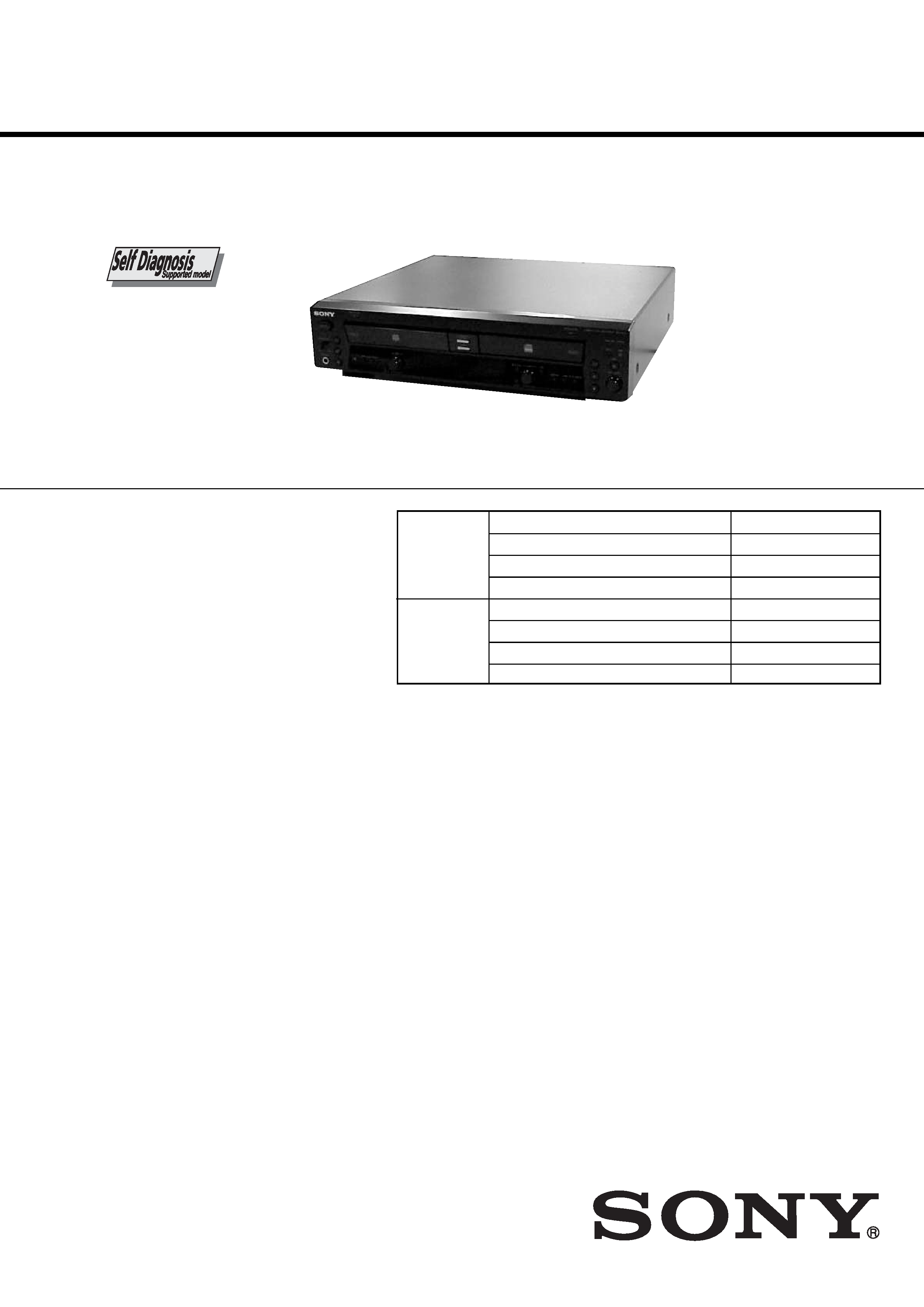
RCD-W10
US Model
Canadian Model
SERVICE MANUAL
COMPACT DISC RECORDER
Sony Corporation
Home Audio Company
Published by Sony Engineering Corporation
9-874-152-01
2002I1600-1
© 2002.09
SPECIFICATIONS
Ver 1.0 2002. 09
Model Name Using Similar Mechanism
NEW
CD Section
CD Mechanism Type
CDM66C-30B61B
Base Unit Type
BU-30BBD61B
Optical Pick-up Type
A-MAX.3
Model Name Using Similar Mechanism
NEW
CD-R/CD-RW CD Mechanism Type
CDM65-RBD1
Section
Base Unit Type
RBD1
Optical Pick-up Type
KRM-220CAA
DECK A (the CD player section)
System
Compact disc digital audio
system
Laser
Semiconductor laser (
=
780 nm)
Emission duration:
continuous
Frequency response
20 Hz 20,000 Hz (
±0.5
dB)
DECK B (the CD-R and CD-RW
recording section)
System
Compact disc digital audio
system
Laser
Semiconductor laser (
=
780 nm)
Emission duration:
continuous
Playable discs
CD, CD-R, CD-RW
Recordable discs
CD-R, CD-RW (for music
use)
Frequency response
20 Hz - 20,000 Hz (
±0.5
dB)
General
Power requirements
North American model:
120 V AC, 60 Hz
Power consumption
25 W
Dimensions (approx.) (w/h/d) incl. projecting parts
and control
430
× 108 × 399 mm
( 17
× 4 3/8 × 15 3/4 inch)
Mass (approx.)
6.0 kg
(13 lbs 4 oz)
Supplied accessories
Design and specifications are subject to change
without notice.
· Audio connecting cords
Phono jack
× 2 (red/white)
Phono jack
× 2 (red/white) (2)
· Remote commander (remote) (1)
· Size AA (R6) batteries (2)
Inputs
ANALOG IN
(Phono jacks)
Impedance: 47 kilohms
Rated input: 500 mVrms
Minimum input
250 mVrms
DIGITAL OPTICAL IN
(Square optical connector jack)
Optical wavelength:
660 nm
Outputs
ANALOG OUT
(Phono jacks)
Impedance: 47 kilohms
Rated output: 2 Vrms
Load impedance: over
10 kilohms
DIGITAL OPTICAL OUT
(Square optical connector jack)
Wavelength: 660 nm
Output level: 18 dBm
PHONES
(Phono jack)
Load impedance: 32 ohms
Output level: 12mW
2
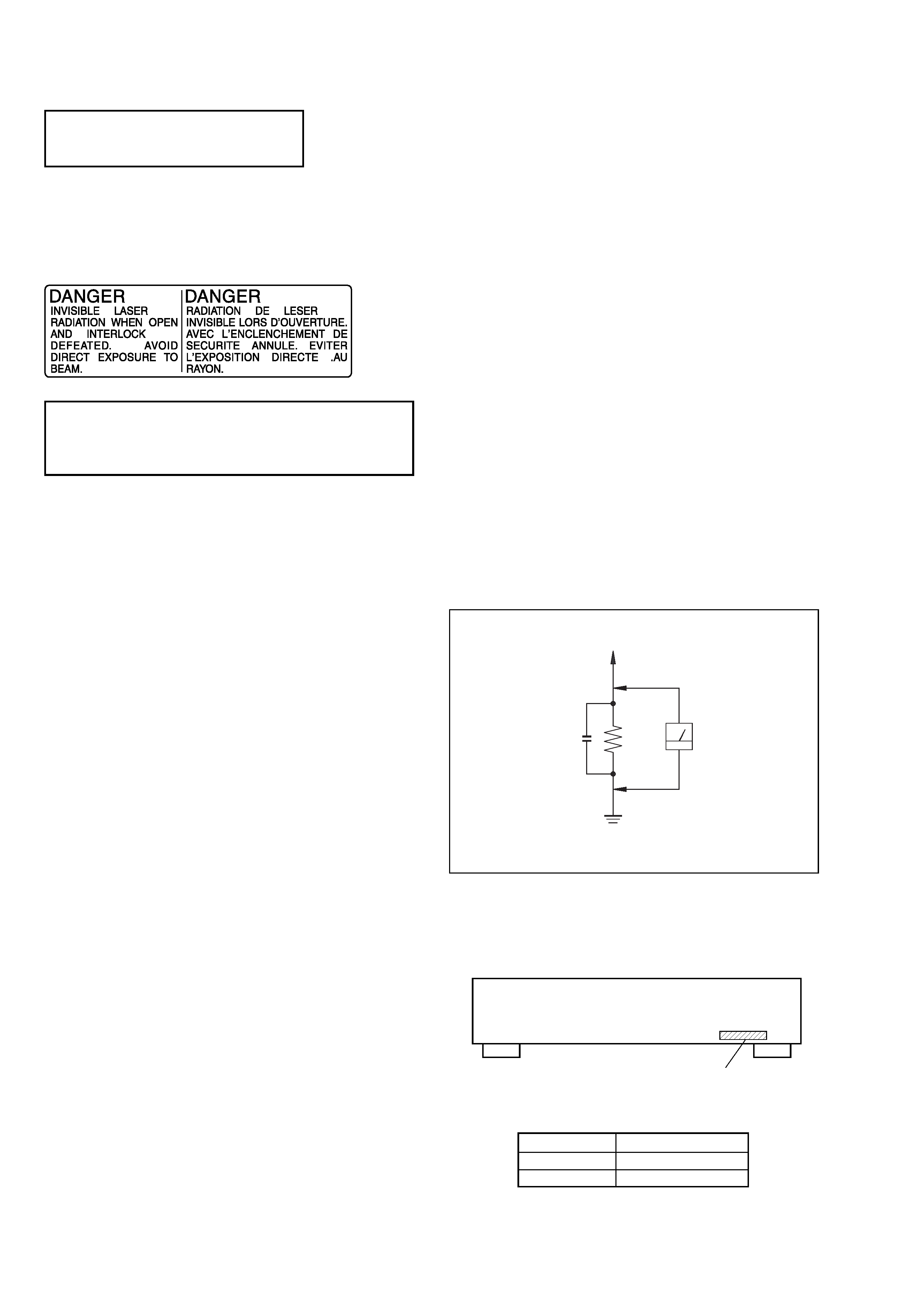
This appliance is classified as a CLASS 1 LASER product. The
CLASS 1 LASER PRODUCT MARKING is located on the rear
exterior.
The following caution label is located inside the apparatus.
Laser component in this product is capable
of emitting radiation exceeding the limit for
Class 1.
CAUTION
Use of controls or adjustments or performance of procedures
other than those specified herein may result in hazardous radiation
exposure.
Notes on chip component replacement
· Never reuse a disconnected chip component.
· Notice that the minus side of a tantalum capacitor may be
damaged by heat.
Flexible Circuit Board Repairing
· Keep the temperature of soldering iron around 270°C
during repairing.
· Do not touch the soldering iron on the same conductor of the
circuit board (within 3 times).
· Be careful not to apply force on the conductor when soldering
or unsoldering.
RCD-W10
SAFETY-RELATED COMPONENT WARNING!!
COMPONENTS IDENTIFIED BY MARK 0 OR DOTTED LINE WITH
MARK 0 ON THE SCHEMATIC DIAGRAMS AND IN THE PARTS
LIST ARE CRITICAL TO SAFE OPERATION. REPLACE THESE
COMPONENTS WITH SONY PARTS WHOSE PART NUMBERS
APPEAR AS SHOWN IN THIS MANUAL OR IN SUPPLEMENTS
PUBLISHED BY SONY.
ATTENTION AU COMPOSANT AYANT RAPPORT
À LA SÉCURITÉ!
LES COMPOSANTS IDENTIFÉS PAR UNE MARQUE 0 SUR LES
DIAGRAMMES SCHÉMATIQUES ET LA LISTE DES PIÈCES SONT
CRITIQUES POUR LA SÉCURITÉ DE FONCTIONNEMENT. NE
REMPLACER CES COMPOSANTS QUE PAR DES PIÈSES SONY
DONT LES NUMÉROS SONT DONNÉS DANS CE MANUEL OU
DANS LES SUPPÉMENTS PUBLIÉS PAR SONY.
After correcting the original service problem, perform the
following safety checks before releasing the set to the customer:
Check the antenna terminals, metal trim, "metallized" knobs, screws,
and all other exposed metal parts for AC leakage. Check leakage as
described below.
LEAKAGE
The AC leakage from any exposed metal part to earth ground and
from all exposed metal parts to any exposed metal part having a
return to chassis, must not exceed 0.5 mA (500 microamperes).
Leakage current can be measured by any one of three methods.
1.
A commercial leakage tester, such as the Simpson 229 or RCA
WT-540A. Follow the manufacturers' instructions to use these
instruments.
2.
A battery-operated AC milliammeter. The Data Precision 245
digital multimeter is suitable for this job.
3.
Measuring the voltage drop across a resistor by means of a
VOM or battery-operated AC voltmeter. The "limit" indication
is 0.75 V, so analog meters must have an accurate low-voltage
scale. The Simpson 250 and Sanwa SH-63Trd are examples of
a passive VOM that is suitable. Nearly all battery operated
digital multimeters that have a 2V AC range are suitable. (See
Fig. A)
SAFETY CHECK-OUT
To Exposed Metal
Parts on Set
0.15
µF
1.5 k
AC
Voltmeter
(0.75 V)
Earth Ground
Fig. A. Using an AC voltmeter to check AC leakage.
MODEL IDENTIFICATION
-- BACK PANEL --
Parts No.
PARTS No.
MODEL
4-238-401-5
4-238-401-6
US
Canadian

3
RCD-W10
TABLE OF CONTENTS
1. SERVICING NOTE ····················································· 4
2. GENERAL ··································································· 5
3. DISASSEMBLY ·························································· 6
3-1. Case (409538) ······························································· 7
3-2. Loading Panel (1CD) ···················································· 7
3-3. Loading Panel (CDR) ··················································· 8
3-4. Front Panel Section ······················································· 8
3-5. DISPLAY Board ··························································· 9
3-6. CDR Mechanism Deck (CDM65-RBD1) ····················· 9
3-7. Tray ············································································· 10
3-8. CDR Board ································································· 10
3-9. Holder (MG) Sub Assy, Dust Cover ··························· 11
3-10. Optical Pick-Up (KRM-220CAA) ······························ 11
3-11. Motor Assy (Loading)(M201) ···································· 12
3-12. Cam (CH) ···································································· 12
3-13. CD Mechanism Deck (CDM66C-30B61B) ················ 13
3-14. Tray (66) ····································································· 14
3-15. BD Board ···································································· 15
3-16. Optical Block Section ················································· 15
3-17. MAIN Board ······························································· 16
4. TEST MODE ···································································· 18
5. ELECTRICAL ADJUSTMENTS ······························· 21
CD SECTION ............................................................. 21
CD-R/RW SECTION .................................................. 22
6. DIAGRAMS ······································································ 53
6-1. Block Diagrams CD-R Section ··························· 54
CD Section ······························· 55
POWER/DISPLAY Section ······ 56
6-2. Printed Wiring Board BD Section ························ 57
6-3. Schematic Diagram BD Section ··························· 58
6-4. Printed Wiring Board CD-R Section (Side A) ······ 59
6-5. Printed Wiring Board CD-R Section (Side B) ······ 60
6-6. Schematic Diagram CD-R Section (1/4) ·············· 61
6-7. Schematic Diagram CD-R Section (2/4) ·············· 62
6-8. Schematic Diagram CD-R Section (3/4) ·············· 63
6-9. Schematic Diagram CD-R Section (4/4) ·············· 64
6-10. Printed Wiring Board MAIN Section (Side A) ····· 65
6-11. Printed Wiring Board MAIN Section (Side B) ····· 66
6-12. Schematic Diagram MAIN Section (1/2) ············· 67
6-13. Schematic Diagram MAIN Section (2/2) ············· 68
6-14. Printed Wiring Board DISPLAY Section ············· 69
6-15. Schematic Diagram DISPLAY Section ················ 70
6-16. IC Block Diagrams ····················································· 71
6-17. IC Pin Function Description ······································· 74
7. EXPLODED VIEWS ······················································ 84
7-1. Case Section ·································································· 84
7-2. Front Panel Section ······················································· 85
7-3. Chassis Section ····························································· 86
7-4. CDR Mechanism Deck Section (CDM65-RBD1) ········ 87
7-5. CD Mechanism Deck Section (CDM66C-30B61B) ····· 88
7-6. Base Unit Section (BU-30BBD61B) ···························· 89
8. ELECTRICAL PARTS LIST ······································· 90
Unleaded solder
Boards requiring use of unleaded solder are printed with the lead-
free mark (LF) indicating the solder contains no lead.
(Caution: Some printed circuit boards may not come printed with
the lead free mark due to their particular size.)
: LEAD FREE MARK
Unleaded solder has the following characteristics.
· Unleaded solder melts at a temperature about 40
°C higher than
ordinary solder.
Ordinary soldering irons can be used but the iron tip has to be
applied to the solder joint for a slightly longer time.
Soldering irons using a temperature regulator should be set to
about 350
°C.
Caution: The printed pattern (copper foil) may peel away if the
heated tip is applied for too long, so be careful!
· Strong viscosity
Unleaded solder is more viscous (sticky, less prone to flow) than
ordinary solder so use caution not to let solder bridges occur such
as on IC pins, etc.
· Usable with ordinary solder
It is best to use only unleaded solder but unleaded solder may
also be added to ordinary solder.

4
RCD-W10
SECTION 1
SERVICING NOTE
NOTES ON HANDLING THE OPTICAL PICK-UP BLOCK
OR BASE UNIT
The laser diode in the optical pick-up block may suffer electrostatic
break-down because of the potential difference generated by the
charged electrostatic load, etc. on clothing and the human body.
During repair, pay attention to electrostatic break-down and also
use the procedure in the printed matter which is included in the
repain parts.
The flexible board is easily damaged and should be handled with
care.
NOTES ON LASER DIODE EMISSION CHECK
The laser beam on this model is concentrated so as to be focused on
the disc reflective surface by the objective lens in the optical pick-
up block. Therefore, when checking the laser diode emission,
observe from more than 30 cm away from the objective lens.
The emission check enables continuous checking of the S curve.
LASER DIODE AND FOCUS SEARCH OPERATION
CHECK
Carry out the "S curve check" in "CD section adjustment" and check
that the S curve waveform is output three times.
Message
C12/
Cannot Copy
C13/
Rec Error
C14/
TOC Error
C41/
Cannot Copy
C71/
Din Unlock
Explanation
You are trying to record a disc that
cannot be played back in DECK-A
or with an external device, such as
CD-ROM or VIDEO CD.
· Remove the disc, and then insert a
music CD for playback.
Recording has not been completed
successfully because of vibration.
· Relocate the unit in a place free of
vibration and restart the recording
again.
The disc you try to record is
excessively dirty (such as oil-
stained or finger marked) or
scratched. Or the disc is not
normal.
· Replace the disc with another one
and restart the recording again.
The unit did not read the TOC
information.
· Insert other discs.
The sound source you are trying to
record is a copy of a commercial
music software. Or you are trying
to record on a CD-R/CD-RW
digitally.
· Because of the restriction of the
Serial Copy Management System,
you cannot record a copy of a
commercial music software.
Neither can you record a CD-R/
CD-RW digitally.
If this message is displayed
momentarily, this is not an error. It
is caused by the digital signal
during recording.
During recording of a digital sound
source, the connecting cable has
been disconnected or the player of
the sound source has turned off.
· Connect the cable or turn on the
digital player.
Self-diagnosis Function
When the self-diagnosis function is activated to
prevent the player from malfunctioning, three
character service numbers in a combination
with a message appears in the display. In this
case, check the following table.
5
RCD-W10
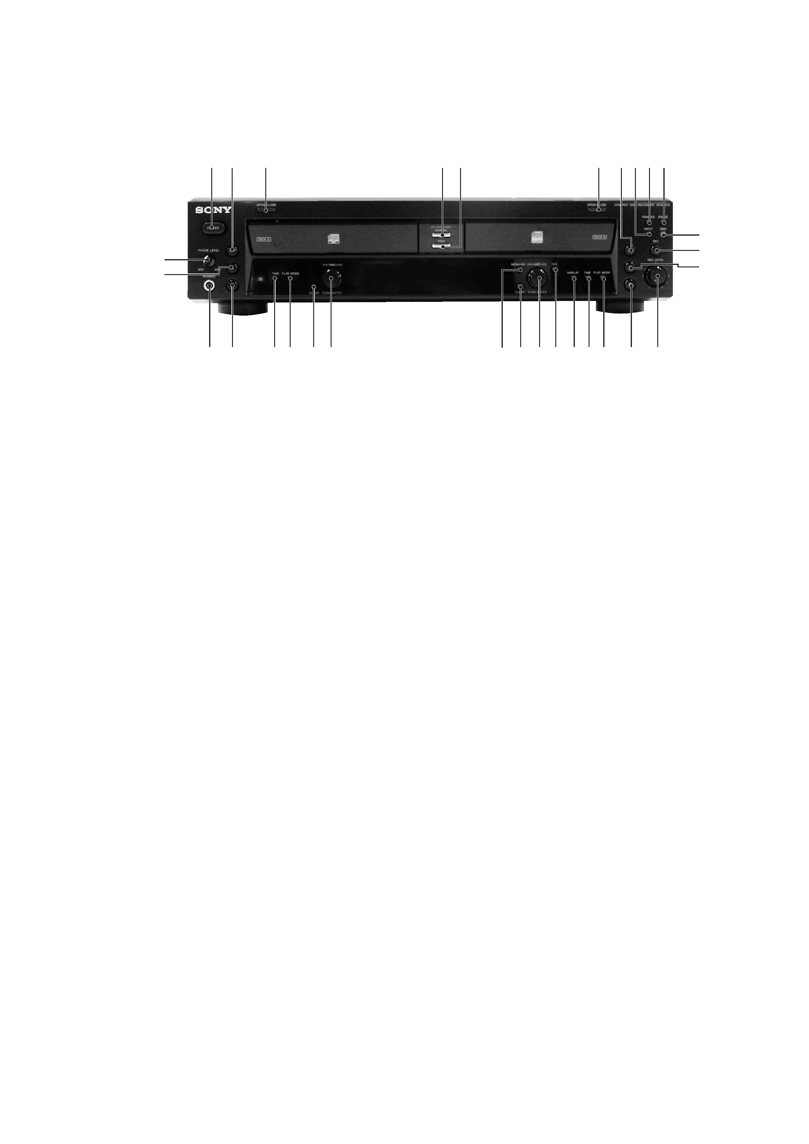
SECTION 2
GENERAL
3
6
4
1 2
5
9
78
q;
qa
qs
qd
qf
qg
qh
qj
qk
ql
w;
wd
wa
wf
wj
wk
e;
wl
wg
wh
ws
1
POWER button
2
H button
3
OPEN/CLOSE A button
4
CD SYNCHRO NORMAL button
5
CD SYNCHRO HIGH button
6
OPEN/CLOSE A button
7
H button
8
INPUT button
9
FINALIZE button
q;
ERASE button
qa
SBM button and indicator
qs
REC z button
qd
X button
qf
REC LEVEL knob
qg
x button
qh
PLAY MODE button
qj
TIME button
qk
DISPLAY button
ql
YES button
w;
l AMS L knob
wa
CLEAR button
ws
MENU/NO button
wd
l AMS L knob
wf
CLEAR button
wg
PLAY MODE button
wh
TIME button
wj
x button
wk
PHONES jack
wl
X button
e;
PHONE LEVEL knob