Conf
idential
SERVICE MANUAL
NOTEBOOK COMPUTER
9-874-581-02
For American Area
Latin Model
· Design and specifications are subject to
change without notice.
PCG-GRX616/GRX626/GRX626P
PCG-GRX717/GRX727
Lineup : PCG-GRX727
PCG-GRX717
PCG-GRX626P
PCG-GRX626
PCG-GRX616
S400
Ver 2-2002J
Revision History
Illust : PCG-GRX717
-- 2 --
Information in this document is subject to change without notice.
Sony, VAIO and CLIE are trademarks or registered trademarks of
Sony. Microsoft, Windows, Windows Media, Outlook, Bookshelf
and other Microsoft products are trademarks or registered trademarks
of Microsoft Corporation in the United States and other countries.
The word Bluetooth and the Bluetooth logo are trademarks of
Bluetooth SIG, Inc. AMD, AMD logo, AMD Duron and
combinations thereof, 3DNow!, are trademarks of Advanced Micro
Devices, Inc. Intel Inside logo, Pentium and Celeron are trademarks
or registered trademarks of Intel Corporation. Transmeta, the
Transmeta logo, Crusoe Processor, the Crusoe logo and
combinations thereof are trademarks of Transmeta Corporation in
the USA and other countries. Graffiti, HotSync, PalmModem, and
Palm OS are resistered trademarks, and the Hotsync logo and Palm
are trademarks of Palm, Inc. or its subsidiaries. (M) and Motrola
are trademarks of Motrora, Inc. Other Motrola products and services
with (R) mark like Dragomball are the trademarks of Motrola, Inc.
All other names of systems, products and services in this manual
are trademarks or registered trademarks of their respective owners.
In this manual, the (TM) or (R) mark are not specified.
Service and Inspection Precautions
1. Obey precautionary markings and instructions
Labels and stamps on the cabinet, chassis, and components identify areas
requiring special precautions. Be sure to observe these precautions, as well
as all precautions listed in the operating manual and other associated
documents.
2. Use designated parts only
The set's components possess important safety characteristics, such as
noncombustibility and the ability to tolerate large voltages. Be sure that
replacement parts possess the same safety characteristics as the originals.
Also remember that the 0 mark, which appears in circuit diagrams and
parts lists, denotes components that have particularly important safety
functions; be extra sure to use only the designated components.
3. Always follow the original design when mounting
parts and routing wires
The original layout includes various safety features, such as inclusion of
insulating materials (tubes and tape) and the mounting of parts above the
printer board. In addition, internal wiring has been routed and clamped so
as to keep it away from hot or high-voltage parts. When mounting parts or
routing wires, therefore, be sure to duplicate the original layout.
4. Inspect after completing service
After servicing, inspect to make sure that all screws, components, and wiring
have been returned to their original condition. Also check the area around
the repair location to ensure that repair work has caused no damage, and
confirm safety.
5. When replacing chip components...
Never reuse components. Also remember that the negative side of tantalum
capacitors is easily damaged by heat.
6. When handling flexible print boards...
· The temperature of the soldering-iron tip should be about 270C.
· Do not apply the tip more than three times to the same pattern.
· Handle patterns with care; never apply force.
Caution: Remember that hard disk drives are easily damaged by
vibration. Always handle with care.
Caution Markings for Lithium/Ion Battery - The following or similar
texts shall be provided on battery pack of equipment or in both the
operating and the service instructions.
CAUTION: Danger of explosion if battery is incorrectly replaced.
Replace only with the same or equivalent type recommended by
the manufacturer. Discard used batteries according to the
manufacturer's instructions.
CAUTION: The battery pack used in this device may present a fire
or chemical burn hazard if mistreated. Do not disassemble, heat
above 100°C (212°F) or incinerate.
Dispose of used battery promptly.
Keep away from children.
CAUTION: Changing the back up battery.
· Overcharging, short circuiting, reverse charging, multilation or
incineration of the cells must be avoided to prevent one or more of
the following occurrences; release of toxic materials, release of
hydrogen and/or oxygen gas, rise in surface temperature.
· If a cell has leaked or vented, it should be replaced immediately
while avoiding to touch it without any protection.
Confidential
PCG-GRX616/GRX626/GRX626P/
PCG-GRX717/GRX727 (AM)

-- 3 --
TABLE OF CONTENTS
CHAPTER 1. BLOCK DIAGRAM ............................... 1-1
(to 1-2)
CHAPTER 2. FRAME HARNESS DIAGRAM ........ 2-1
(to 2-2)
CHAPTER 3. EXPLODED VIEWS AND
PARTS LIST ............................................ 3-1
3-1. Main Section .................................................................... 3-3
3-2. LCD Section (GRX717/GRX727) Made by HI ........ 3-7
3-3. LCD Section (GRX616/GRX626/GRX626P)
Made by HI ................................................................. 3-9
3-4. Connector Section (CH Type only) ............................... 3-11
(to 3-12)
CHAPTER 4. OTHERS
4-1. Replacing the CPU .......................................................... 4-1
1. Removing the CPU .......................................................... 4-1
2. Installing the CPU ............................................................ 4-1
Section
Title
Page
Confidential
History of the changes is shown as the
"Revision History" at the end of this data.
PCG-GRX616/GRX626/GRX626P/
PCG-GRX717/GRX727 (AM)
Confidential
PCG-GRX616/GRX626/GRX626P/
PCG-GRX717/GRX727 (AM)
(END)
1-2
1-1
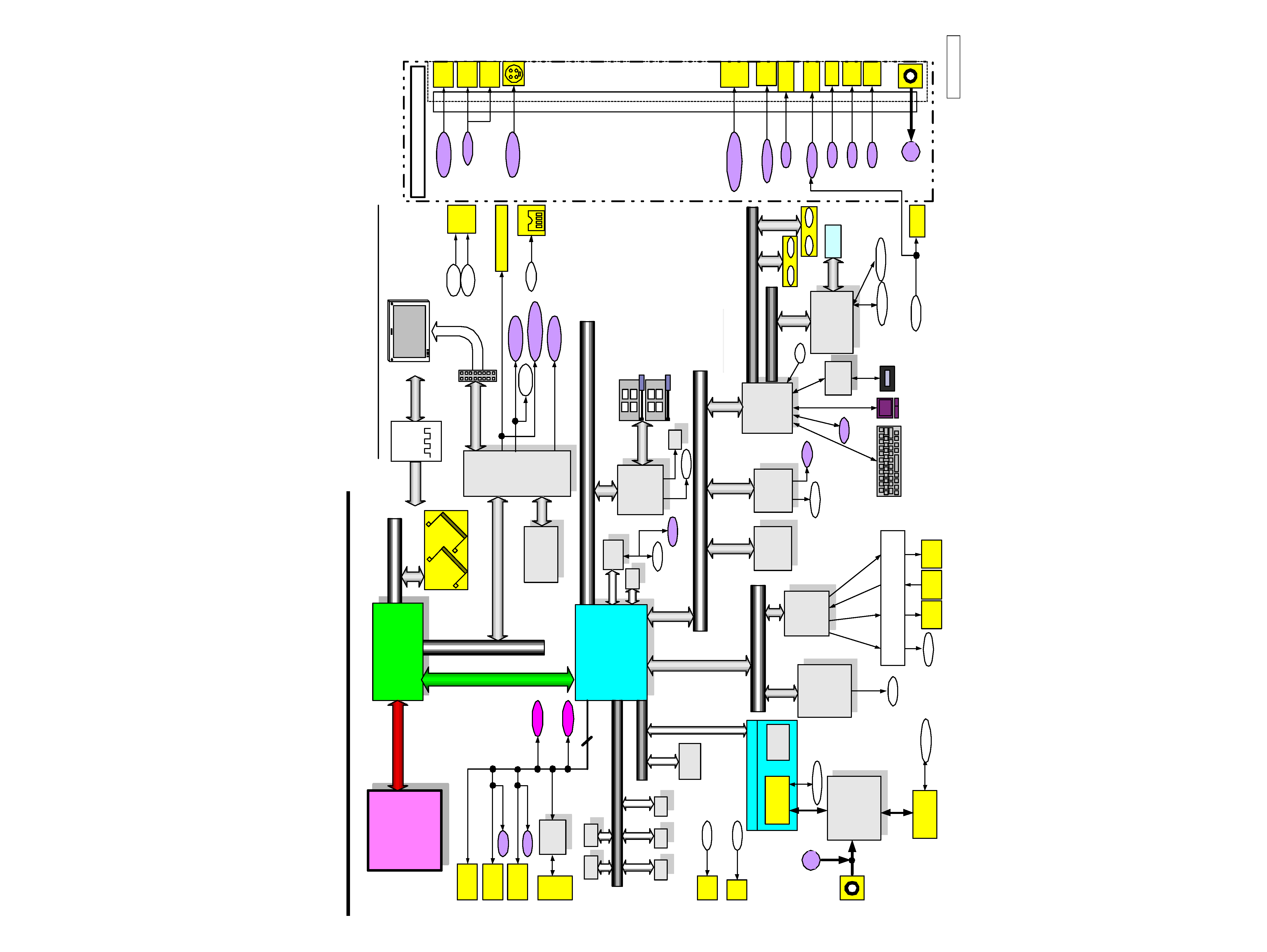
CHAPTER 1.
BLOCK DIAGRAM
Video Memory
K4D623238B
x 2pcs
Video Memory
K4D623238B
x 2pcs
Memory
CONTROLLER
HUB (MCH)
593 FCBGA
Memory
CONTROLLER
HUB (MCH)
593 FCBGA
IO Control H ub
ICH3-m
FW82801CAM
IO Control Hub
ICH3-m
FW82801CAM
Internal
HDD
PCG-GRX Series BLOCK DIAGRAM Rev.0.10
PHONE
OUT
RJ11
MIC
IN
RJ45
MS
CONN
Pentium 4
Processor
512KB L2
478pins
uFCPGA
Pentium 4
Processor
512KB L2
478pins
uFCPGA
PCI BUS(3.3V)
A
GP
x
4
266 MHz Memory Bus
(DDR)
CardB us/16bitCard
PC Card
Connector
2 Slot
H8S/2149
KBC/EC
SPIC
H8S/2149
KBC/EC
SPIC
Graphics
M7-P
(ATI)
Graphics
M7-P
(ATI)
LCD CONN
Cable
Ether
PHY
Ether
PHY
Internal KeyBoard
Membra ne
JOG
Controller
JOG
Controller
VGA DSUB-15
LPC
Memory
Stick
Module
Memory
Stick
Module
i.LINK0
AC LINK
He
adphone
MIC
Spea
ker
Speaker
L&R
Super I/O
SMsC
LPC47N227
Super I/O
SMsC
LPC47N227
I/O Expander
& SMBUS MUX
I/O Expander
& SMBUS MUX
LID
Seri al
Parallel
Refer to Clock Generator
Block Diagram
SMBUS2
USB Right
CONN
TouchPad
JOG
EEPROM
EEPROM
For VID
EEPROM
EEPROM
For i.LINK
MDC
(Modem
Daughter
Card)
Module
MDC
(Modem
Daughter Card)
Module
CPU Local Bus
EEPROM
EEPROM
For Password
USB Left
CONN
USB Rear
CONN
i.LINK
Dock-VGA D B-15
Dock-VGA D B-15
Seri al
Parallele
RJ-45
RJ45
VGA
DB-15
Video-
Out
USB
CONN
USB
CONN
LineOut
Port0-5
Optical
Drive
Pr
imary
Secondary
ID E(ATA100)
AMP, etc.
Line
Out
RJ-45
RJ-45
Parallel
PS/2
CLKGEN
IMI
9870GTD
Port Repricator
Parallel
Paral lele
i.LINK0
Port-4
Port-0
Port-3
Port-2
Port-1
Port-5
RJ-45
RJ-11
RJ-11
1st
Battery
Power
Circuit
Power
Circuit
DC Jack
DDR(SO-DIMM)
SMBUS2
SMBUS2
SMBUS1
SMBUS0
PS/2
Reserved
Reserved
Port-3
Port-2
DC Jack
Serial
DCin
DCin
BATTERY1
BATTERY2
BATTERY1
2nd
Battery
BATTERY2
FAN0
AT F0
FAN1
AT F1
PS/2
Other
Control
DDR(SDRAM)
FWH
8Mb
(Flas h BIOS
ROM)
FWH
8Mb
(Flas h BIOS
ROM)
Multi PurposeBay
LINE-OUT
AV
Out
Audio-Out
S-Video-Out
Audio
L-out
Audio
R-out
TV-O ut
TV-O ut
S-Video-Out
TV-O ut
USB3
USB2
USB3
USB2
Audio
YMF753
(Yamaha)
Audio
YMF753
(Yamaha)
SONY
TV-O ut
CARDBUS
& i.LINK
RICOH
R5C552
CARDBUS
& i.LINK
RICOH
R5C552
Bus #2 Dev #5
EEPROM
EEPROM
For LAN
EEPROM
EEPROM
For Clock GEN
EEPROM
On DIMM1
EEPROM
On DIMM1
For SPD
EEPROM
On DIMM2
EEPROM
On DIMM2
For SPD
16inch UXGA
15inch XGA
Confidential
PCG-GRX616/GRX626/GRX626P/
PCG-GRX717/GRX727 (AM)
2-2
2-1
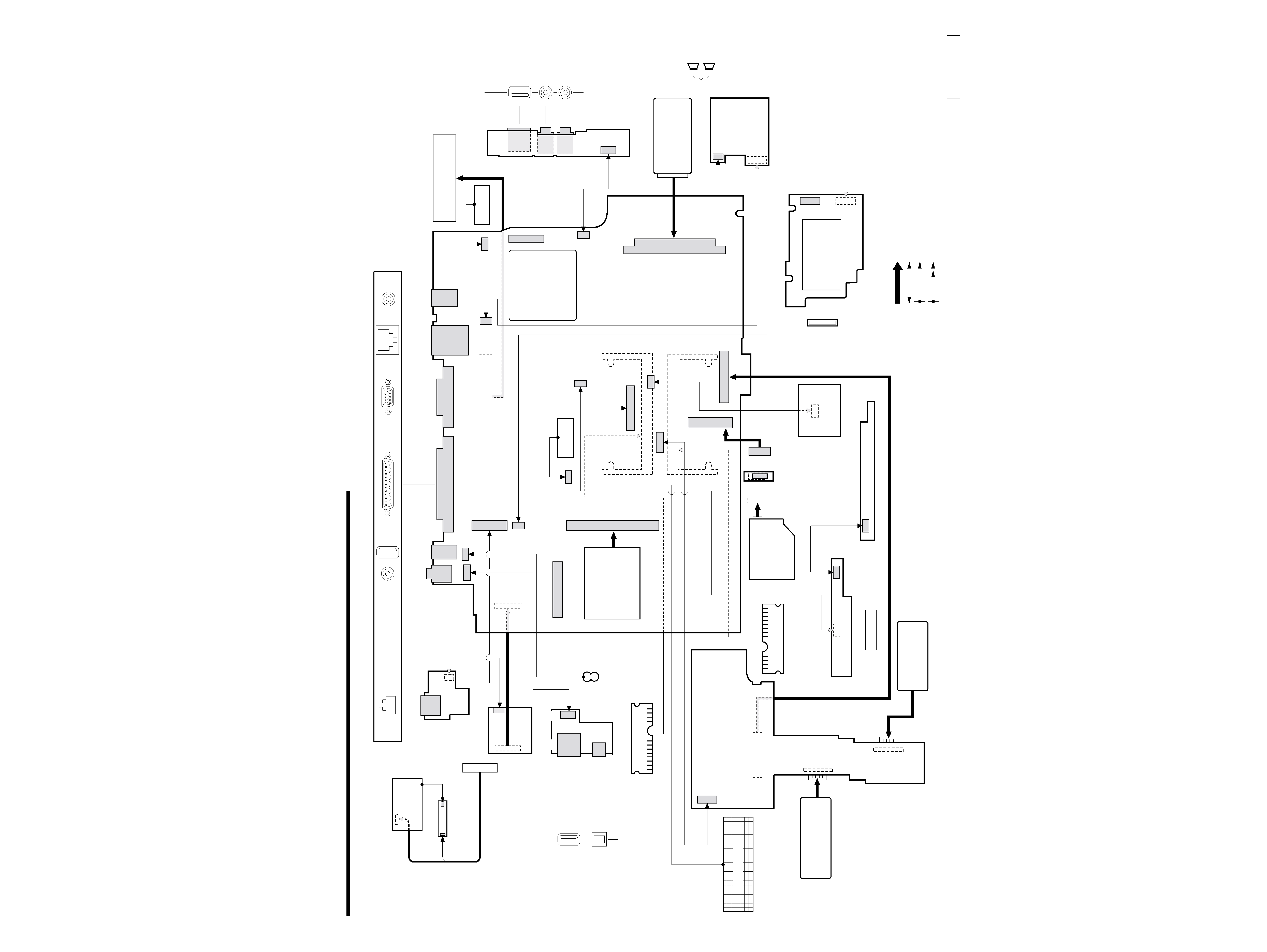
CHAPTER 2.
FRAME HARNESS DIAGRAM
CN8001
39
40
1
2
CN8402
IEEE 1394 i.LINK
CPU
PWS-17 Board
(Side-B)
BATTERY PACK
CN8401
2nd BATTERY PACK
(OPTION)
From board to connector (direct connection)
Harness (connector at both end)
Harness (soldered at one end)
Connectors soldered on board and appearing on the panel
PHONE
PRINTER
NETWORK
MONITOR
DC-IN
USB
AV OUT
HARD DISK
44
1
2
13
14
2
43
1
CN2201
CN1126
PC CARD
CONNECTOR
CN1202
CN8002
77
1
78
154
13
9
40
2
CN7501
CN7001
CN7002
CN4001
2
1
50
49
60
59
2
1
CN2301
Combination
DRIVE
CNX-161 Board
(Side-A)
LEX-34 Board
(Side-A)
SWX-91 Board
(Side-A)
SWX-111 Board
(Side-A)
IFX-193 Board
(Side-A)
CNX-158 Board
(Side-A)
CNX-159 Board
(Side-A)
CNX-157 Board
(Side-A)
CN7502
59
60
1
2
1
1
4
12
1
12
1
1
2
21
22
1
2
CN3102
CN1601
1
1
2
2
29
30
MODEM
CARD
J1
1
2
29
30
CN1301
CN851
CN855
CN1111
CN1501
CN3501
CN2005
CN2007
CN101
2
1
NICKEL HYDROGEN
BATTERY
CN3101
CN852
22
8
27
1
CN3004
120
2
1
119
CN1401
11
1
2
12
CN1124
11
1
21
2
12
1
12
1
1
20
12
CN2001
CN5001
HARNESS
(2P)
CN5602
CN5603
CN5601
MBX-65 Board
(Side-A)
199
200
1
24
1
31
42
14
2
13
1
10
1
10
1
114
1
1
2
19
20
199
2
2
200
CN501
CN6002
CN6001
CN4691
CN4602
CN502
CN3103
CN1901
CN853
CN2901
99
100
1
2
PCGA-PRGX1
Port Replicator
FFC
CN5530
CN5510
CN5540
1
14
CN5500
FFC
USB
EXTERNAL
MICROPHONE
HEADPHONE
USB
LCD HARNESS
INVERTER
LCD
21
SPEAKER
MEMORY
STICK
L Side
L Side
R Side
CN4601
RAM
RAM
DDR266 SO-DIMM
256MB
DDR266 SO-DIMM
256MB
KEY BOARD
Rear Panel
12
1
TOUCH PAD
J1
DC FAN
2nd FAN
JOG DIAL
CN2009
(END)