SERVICE MANUAL
NVA-CU3/CU3T
Ver. 1.0 2005.12
SPECIFICATIONS
9-879-986-01
2005L05-1
© 2005.12
Sony Corporation
eVehicle Division
Published by Sony Engineering Corporation
US Model
Canadian Model
NVA-CU3
AEP Model
UK Model
NVA-CU3/CU3T
Operating temperature:
5 45 ºC (41 113 ºF)
Power requirements:
DC 5.2 V
(from supplied 12 V car battery adapter (negative
earth))
Connection terminals:
Unit connector
DC IN 5.2V jack
TMC antenna(aerial) jack (NVA-CU3T only)
Reception frequency:
87.5 108.0 MHz
(NVA-CU3T only)
· Car battery adapter (1)
· TMC antenna (aerial) jack (1)/suction cups (2)
(For NVA-CU3T)
· Mounting plate (1)
(For NVA-CU3 (US and Canadian models))
· Screwes (3)
(For NVA-CU3 (US and Canadian models))
· Adhesive tape (1)
· Pad (1)
Supplied accessories
Design and specifications are subject to change
without notice.
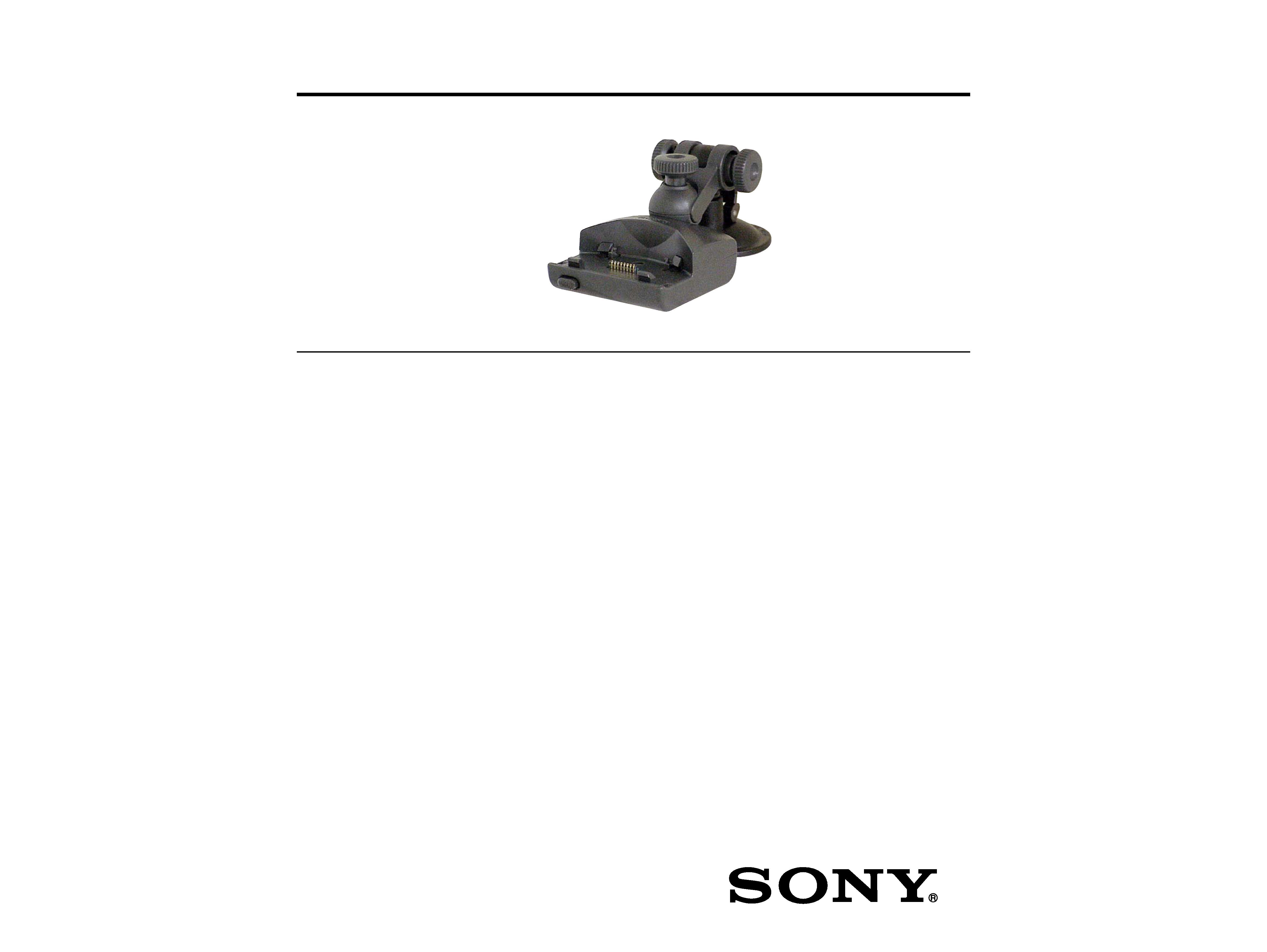
Photo: NVA-CU3T
Notes on chip component replacement
· Never reuse a disconnected chip component.
· Notice that the minus side of a tantalum capacitor may be
damaged by heat.
NVA-CU3
CAR CRADLE KIT
NVA-CU3T
TMC CAR CRADLE KIT
2
NVA-CU3/CU3T
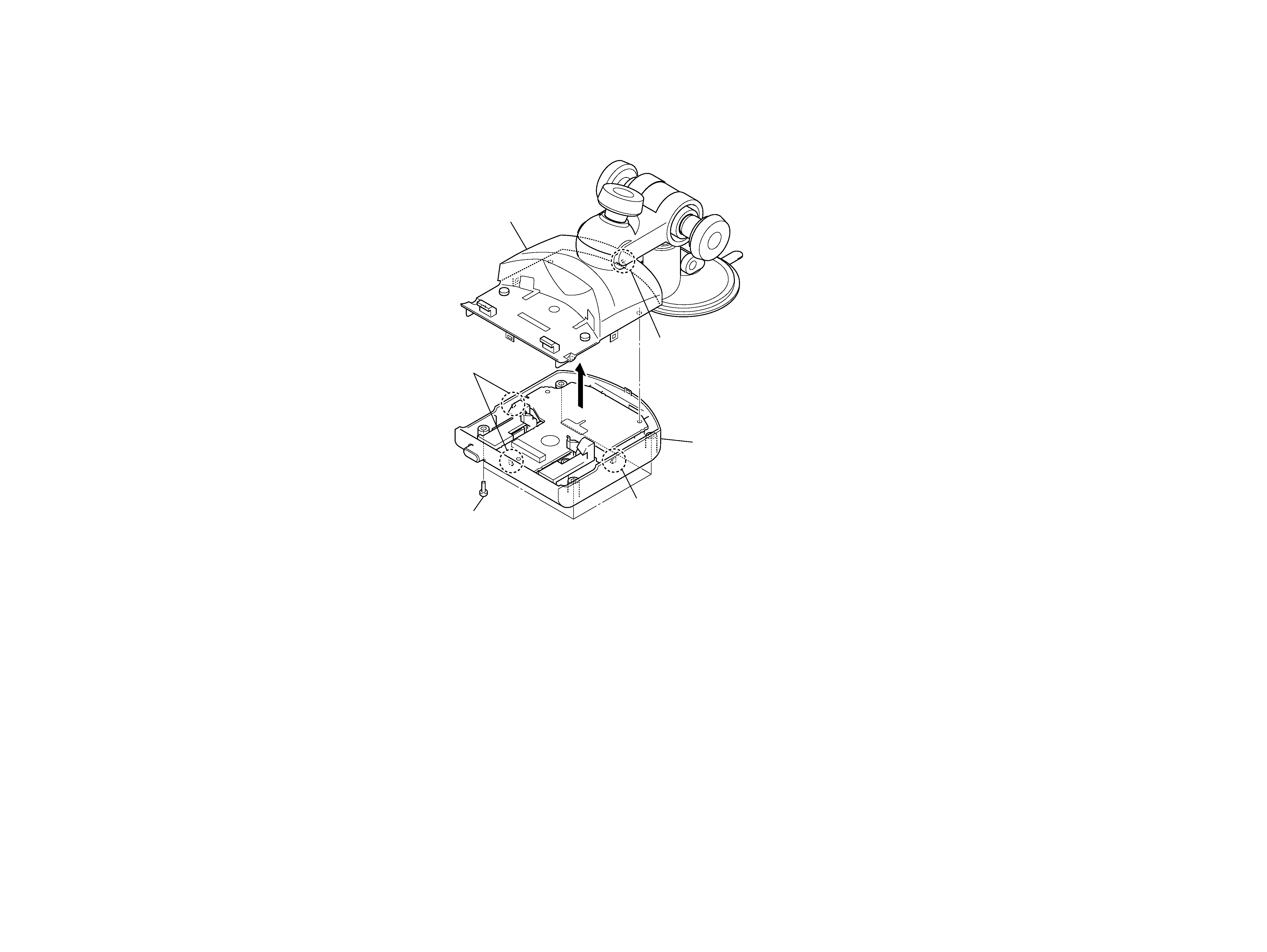
Note: Follow the disassembly procedure in the numerical order given.
CASE (UPPER) BLOCK ASSY, CASE (LOWER) BLOCK ASSY
SECTION 1
DISASSEMBLY
1
four screws
(B2
× 5)
2
claw
3
case (upper) block assy
4
case (lower) block assy
2
claw
2
two claws

3
NVA-CU3/CU3T
SECTION 2
DIAGRAMS
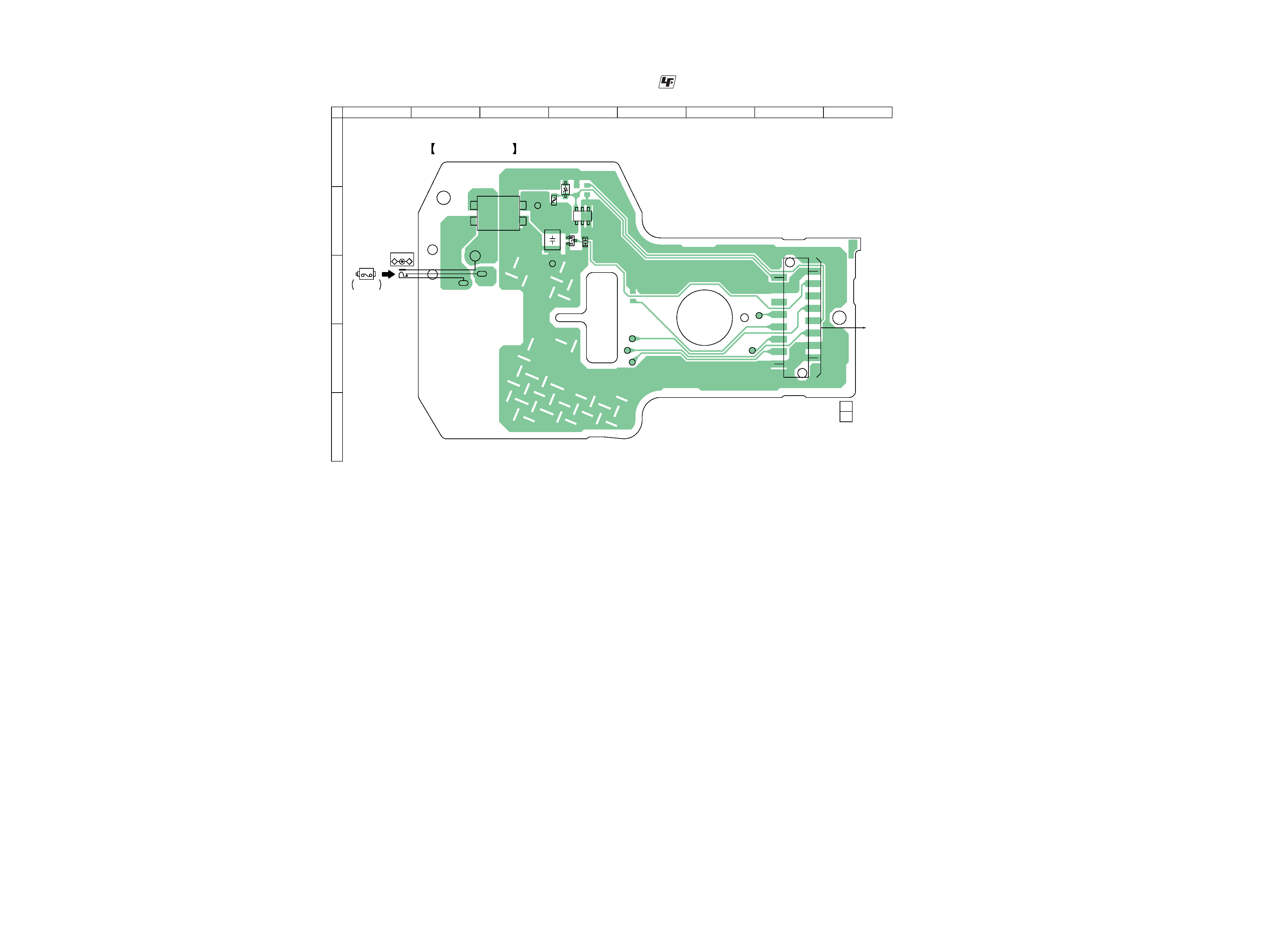
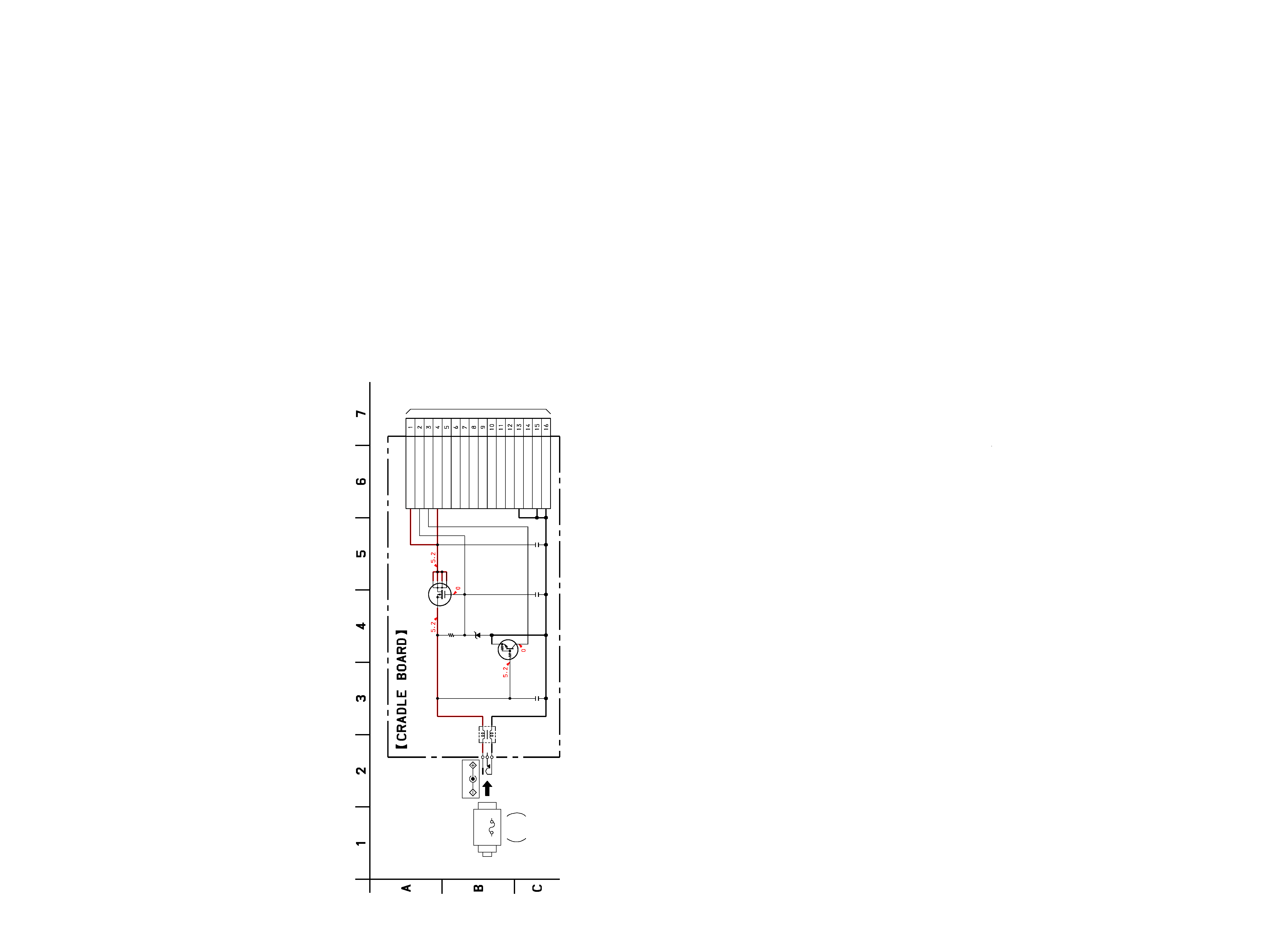
· Note for Printed Wiring Boards and Schematic Diagrams
Note on Schematic Diagram:
· All capacitors are in µF unless otherwise noted. (p: pF)
50 WV or less are not indicated except for electrolytics
and tantalums.
· All resistors are in and 1/4 W or less unless otherwise
specified.
· C : panel designation.
· A : B+ Line.
· Power voltage is dc 5.2V and fed with regulated dc power
supply from DC jack on the CRADLE board (J1001).
· Voltages is dc with respect to ground under no-signal con-
ditions.
no mark : POWER ON
· Voltages are taken with a VOM (Input impedance 10 M).
Voltage variations may be noted due to normal produc-
tion tolerances.
· Signal path.
f
: FM
Note on Printed Wiring Board:
· X : parts extracted from the component side.
· Y : parts extracted from the conductor side.
·
: Pattern from the side which enables seeing.
(The other layers' patterns are not indicated.)
Caution:
Pattern face side:
Parts on the pattern face side seen from
(Side B)
the pattern face are indicated.
Parts face side:
Parts on the parts face side seen from
(Side A)
the parts face are indicated.
4
NVA-CU3/CU3T
2-1. PRINTED WIRING BOARD CRADLE Board (CU3)
Q1002
Q1001
CN1001
TO
MAIN UNIT
R1001
C1001
C1003
TP1007
TP1008
TP1011
TP1012
TP1014
LF1001
JL1001
JL1002
D1001
J1001
DC IN 5.2V
+
CRADLE BOARD
1-869-172-
11
(11)
F1001
CIGAR
LIGHTER PLUG
A
B
C
D
E
1
2
3
4
5
6
7
8
D
D
G
D
D
S
1
2
16
15
: Uses unleaded solder.
NVA-CU3/CU3T
5
5
2-2. SCHEMATIC DIAGRAM CRADLE Board (CU3)
LF1001
C1002
C1003
R1001
D1001
Q1002
CN1001
Q1001
C1001
F1001
0.1
0.01
100k
MM3Z6V8ST1
DTC144EET1
16P
RSQ035P03TR
10
2A 5.2V
ADP_5V
CRADLE_ON
ACC_CHECK
ADP_5V
TU_5V
NAVI_ATT
RDS_DET1
TU_GND
GPS_TXD
RDS_DET2
RDS_TXD
GPS_RXD
GND
RDS_RXD
CRADLE_ON_GND
GND
B+ SWITCH
ACCESSORY
DETECT
S
CIGER
LIGHTER
PLUG
(TO MAIN UNIT)
J1001
DC IN 5.2V