SERVICE MANUAL
DIGITAL STILL CAMERA
LEVEL
3
Link
SCHEMATIC DIAGRAMS
PRINTED WIRING BOARDS
REPAIR PARTS LIST
ADJUTMENTS
DISASSEMBLY
SCHEMATIC DIAGRAMS
PRINTED WIRING BOARDS
REPAIR PARTS LIST
ADJUTMENTS
DISASSEMBLY
Link
Revision History
Revision History
The information that is not described in this Service Manual is described
in the LEVEL 2 Service Manual.
When repairing, use this manual together with LEVEL 2 Service Manual.
Contents of LEVEL 2 Service Manual
1. SERVICE NOTE
2. DISASSEMBLY
3. BLOCK DIAGRAMS
4. PRINTED WIRING BOARDS AND
SCHEMATIC DIAGRAMS
5. ADJUSTMENTS
6. REPAIR PARTS LIST
OVERALL
POWER
CD-440, PK-069, CK-133, FU-164
BOARD,CONTROL SWITCH
BLOCK (RS-310), FLASH UNIT,
FP-461, FP-462 FLEXIBLE
EXPLODED VIEWS
ELECTRICAL PARTS LIST
· For INSTRUCTION MANUAL, refer to SERVICE MANUAL, LEVEL 1 (987622541.pdf).
· Reference No. search on printed wiring boards is available.
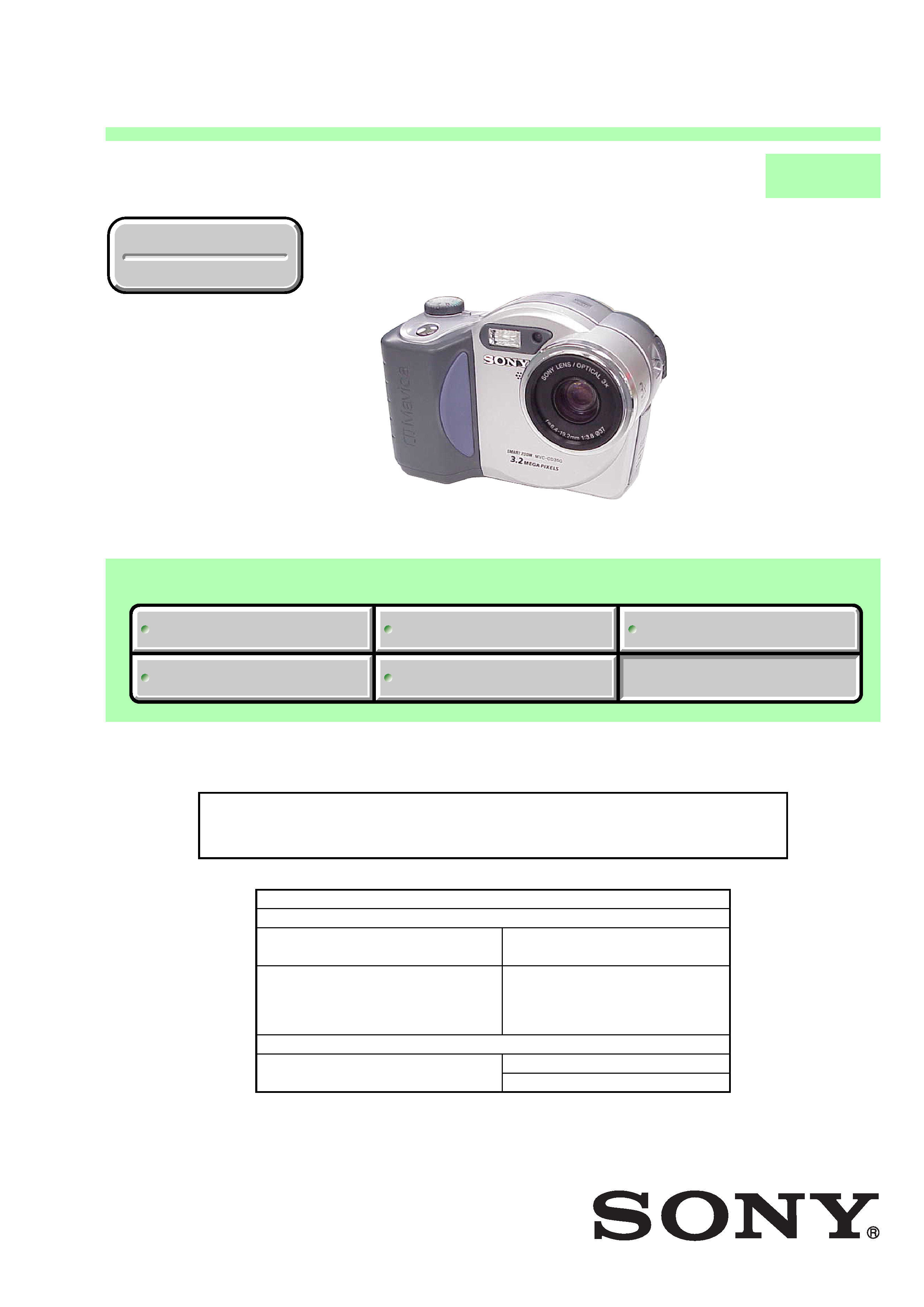
MVC-CD350
US Model
Ver 1.0 2003. 04
-- 2 --
MVC-CD350
1.
Check the area of your repair for unsoldered or poorly-soldered
connections. Check the entire board surface for solder splashes
and bridges.
2.
Check the interboard wiring to ensure that no wires are
"pinched" or contact high-wattage resistors.
3.
Look for unauthorized replacement parts, particularly
transistors, that were installed during a previous repair. Point
them out to the customer and recommend their replacement.
4.
Look for parts which, through functioning, show obvious signs
of deterioration. Point them out to the customer and
recommend their replacement.
5.
Check the B+ voltage to see it is at the values specified.
6.
Flexible Circuit Board Repairing
· Keep the temperature of the soldering iron around 270°C
during repairing.
· Do not touch the soldering iron on the same conductor of the
circuit board (within 3 times).
· Be careful not to apply force on the conductor when soldering
or unsoldering.
Unleaded solder
Boards requiring use of unleaded solder are printed with the lead-
free mark (LF) indicating the solder contains no lead.
(Caution: Some printed circuit boards may not come printed with
the lead free mark due to their particular size.)
: LEAD FREE MARK
Unleaded solder has the following characteristics.
· Unleaded solder melts at a temperature about 40°C higher than
ordinary solder.
Ordinary soldering irons can be used but the iron tip has to be
applied to the solder joint for a slightly longer time.
Soldering irons using a temperature regulator should be set to
about 350°C.
Caution: The printed pattern (copper foil) may peel away if the
heated tip is applied for too long, so be careful!
· Strong viscosity
Unleaded solder is more viscous (sticky, less prone to flow) than
ordinary solder so use caution not to let solder bridges occur such
as on IC pins, etc.
· Usable with ordinary solder
It is best to use only unleaded solder but unleaded solder may
also be added to ordinary solder.
SAFETY CHECK-OUT
After correcting the original service problem, perform the following
safety checks before releasing the set to the customer.
SAFETY-RELATED COMPONENT WARNING!!
COMPONENTS IDENTIFIED BY MARK 0 OR DOTTED LINE WITH
MARK 0 ON THE SCHEMATIC DIAGRAMS AND IN THE PARTS
LIST ARE CRITICAL TO SAFE OPERATION. REPLACE THESE
COMPONENTS WITH SONY PARTS WHOSE PART NUMBERS
APPEAR AS SHOWN IN THIS MANUAL OR IN SUPPLEMENTS
PUBLISHED BY SONY.
ATTENTION AU COMPOSANT AYANT RAPPORT
À LA SÉCURITÉ!
LES COMPOSANTS IDENTIFÉS PAR UNE MARQUE 0 SUR LES
DIAGRAMMES SCHÉMATIQUES ET LA LISTE DES PIÈCES SONT
CRITIQUES POUR LA SÉCURITÉ DE FONCTIONNEMENT. NE
REMPLACER CES COMPOSANTS QUE PAR DES PIÈSES SONY
DONT LES NUMÉROS SONT DONNÉS DANS CE MANUEL OU
DANS LES SUPPÉMENTS PUBLIÉS PAR SONY.
COVER
COVER
CAUTION :
Danger of explosion if battery is incorrectly replaced.
Replace only with the same or equivalent type.
WARNING!!
WHEN SERVICING, DO NOT APPROACH THE LASER
EXIT WITH THE EYE TOO CLOSELY. IN CASE IT IS
NECESSARY TO CONFIRM LASER BEAM EMISSION,
BE SURE TO OBSERVE FROM A DISTANCE OF MORE
THAN
30
cm
FROM THE
SURFACE
OF THE
OBJECTIVE LENS ON THE OPTICAL PICK-UP BLOCK.
CAUTION:
The use of optical instrument with this product will increase eye
hazard.
CAUTION
Use of controls or adjustments or performance
procedures other than those specified herein may
result in hazardous radiation exposure.

-- 3 --
MVC-CD350
TABLE OF CONTENTS
2.
DISASSEMBLY
2-18. SY-087 BOARD ···························································· 2-17
2-19. BU ASSEMBLY ···························································· 2-18
2-20. OPTICAL DEVICE ······················································ 2-19
2-21. DC MOTOR (SLED) ····················································· 2-20
2-22. DC MOTOR (SPINDLE) ·············································· 2-20
4.
PRINTED WIRING BOARDS AND
SCHEMATIC DIAGRAMS
4-2.
SCHEMATIC DIAGRAMS
· SY-087 (1/11)(CAMERA MODULE)
SCHEMATIC DIAGRAM ···························· 4-23
· SY-087 (2/11)(LENS DRIVE)
SCHEMATIC DIAGRAM ···························· 4-25
· SY-087 (3/11)(CAMERA DSP, VIDEO AMP)
SCHEMATIC DIAGRAM ···························· 4-27
· SY-087 (4/11)(MC CAM, SH DSP, CLK GEN.)
SCHEMATIC DIAGRAM ···························· 4-29
· SY-087 (5/11)(FLASH ROM)
SCHEMATIC DIAGRAM ···························· 4-31
· SY-087 (6/11)(CD-R/RW, DSP)
SCHEMATIC DIAGRAM ···························· 4-33
· SY-087 (7/11)(OPTICAL RF SERVO/DRIVE)
SCHEMATIC DIAGRAM ···························· 4-35
· SY-087 (8/11)(HI CONTROL)
SCHEMATIC DIAGRAM ···························· 4-37
· SY-087 (9/11)(AUDIO AMP)
SCHEMATIC DIAGRAM ···························· 4-39
· SY-087 (10/11)(CONNECTOR)
SCHEMATIC DIAGRAM ···························· 4-41
· SY-087 (11/11)(CONNECTOR, DC SUPPLY)
SCHEMATIC DIAGRAM ···························· 4-43
4-3.
PRINTED WIRING BOARDS
· SY-087 (CAMERA MODULE, LENS DRIVE,
CAMERA DSP, VIDEO AMP, MC CAM, SH DSP,
CLK GEN., FLASH ROM, CD-R/RW, DSP, OPTICAL
RF SERVO/DRIVE, HI CONTROL, AUDIO AMP,
CONNECTOR, DC SUPPLY)
PRINTED WIRING BOARD ······················· 4-57
4-4.
WAVEFORMS ······························································ 4-68
4-5.
MOUNTED PARTS LOCATION ································· 4-70
5.
REPAIR PARTS LIST
5-1.
EXPLODED VIEWS ······················································ 5-8
5-1-6. DDX-G3000 COMPLETE SECTION ···························· 5-8
5-1-7. BU SECTION ·································································· 5-9
5-2.
ELECTRICAL PARTS LIST ········································ 5-14
6.
ADJUSTMENTS
1.
Before starting adjustment ··············································· 6-1
6-3.
ADJUSTMENT
(DDX-G3000 COMPLETE ASSEMBLY) ···················· 6-45
1.
Adjusting items when replacing main parts and boards ·· 6-45
2.
List of Service Tools ······················································ 6-46
3.
Error Analysis and Repair Work Flow ··························· 6-47
3-1.
Save the Error Status ····················································· 6-47
1.
Execute [Error Log File]. ·············································· 6-47
2.
Execute [EEPROM Menu]. ··········································· 6-47
3-2.
Analyze and Repair the Errors due to
Mechanical Causes ························································ 6-47
1.
Check the outside appearance for defects. ···················· 6-47
2.
Check operations of the machine for any defective
operation. ······································································· 6-47
3-3.
Analyze and Repair the Errors due to Electrical Causes ·· 6-47
1.
Perform the electrical adjustments to locate and
analyze the cause of error. ············································· 6-47
2.
Adjustments after the OP (Optical device) is replaced · 6-47
4.
Attaching the BU to the BU base for adjustment ·········· 6-48
5.
Connecting the equipment ············································· 6-50
5-1.
Optical Power Meter ······················································ 6-51
5-2.
Jitter Meter ···································································· 6-52
5-3.
Personal computer ························································· 6-52
6.
Installing the "Dencho for CD350 & CD500" ·············· 6-52
7.
Adjustment ···································································· 6-53
7-1.
Switch Setting during Adjustments ······························· 6-53
7-2.
Starting Up "Dencho for CD350 & CD500" ················· 6-54
7-3.
Saving the Error Status and Initializing the EEPROM ·· 6-55
7-3-1. Saving the Error Log File ·············································· 6-55
7-3-2. Saving the EEPROM Data ············································ 6-56
7-3-3. Initializing the EEPROM ·············································· 6-56
7-4.
Laser Power Adjustment ················································ 6-57
7-5.
SKEW Adjustment ························································ 6-60
7-6.
CDR Adjustment ··························································· 6-61
7-7.
CDRW Adjustment ························································ 6-61
7-8.
Home Position Setting ··················································· 6-62
7-9.
Description of the Adjustment Menu (Engineer mode)
Screen ············································································ 6-63
7-10. Description of the EEPROM Screen ····························· 6-64
6-4.
TROUBLESHOOTING (DDX-G3000) ························ 6-65
1.
FLOW OF TROUBLE ANALYSIS AND REPAIR ······ 6-65
2.
DENCHO FOR DDX-G3000 MENU ··························· 6-67
3.
TROUBLESHOOTING THE DDX-G3000 ·················· 6-69
1.
Laser Power Adjust ························································ 6-70
1-1.
Read Power
t NG ······················································· 6-70
1-2.
Write Power
t NG ······················································ 6-70
2.
SKEW Adjust ································································ 6-70
2-1.
SKEW Adjust
t NG (Judgment is not performed) ····· 6-70
3.
CDR Adjust ··································································· 6-71
3-1.
Adjust FE
t NG ·························································· 6-71
3-2.
RF Gain
t NG ····························································· 6-71
3-3.
TE Gain Offset
t NG ·················································· 6-71
3-4.
DPP (Differential Push-Pull: One of the Tracking
Error Detection Methods) Balance
t NG ··················· 6-71
3-5.
Focus Gain, Tracking Gain
tNG ································ 6-71
3-6.
Seek Check
t NG ······················································· 6-71
3-7.
Adjust WFB
t NG (Judgment is not performed.) ······· 6-71
3-8.
ATER (Absolute Time in pre-groove Error Rate)
Check
t NG ································································ 6-71
3-9.
Focus Bias ATIP (Absolute Time In Pre-groove)
t NG (Judgment is not performed.) ···························· 6-72
3-10. Read b After ATER
t NG ··········································· 6-72
3-11. Self RF Jitter
t NG (Judgment is not performed.) ····· 6-72
4.
CDRW Adjust ································································ 6-72
4-1.
RW FE
t NG ······························································· 6-72
4-2.
RW RF Gain
t NG ······················································ 6-72
4-3.
Focus Gain, Tracking Gain
t NG ······························· 6-73
4-4.
Erase Power Gain
t NG ·············································· 6-73
4-5.
ATER (Absolute Time in pre-groove Error Rate)
Check
t NG ································································ 6-73
4-6.
After ATER
t NG ······················································· 6-73
4-7.
BLER (Block Error Rate) Check
t NG ······················ 6-73
4-8.
Self RF Jitter
t NG (Judgment is not performed.) ····· 6-73
4.
THE AREAS THAT TEND TO BREAK
DOWN WHEN DROPPED TO GROUND ··················· 6-74
2-17
SECTION 2
DISASSEMBLY
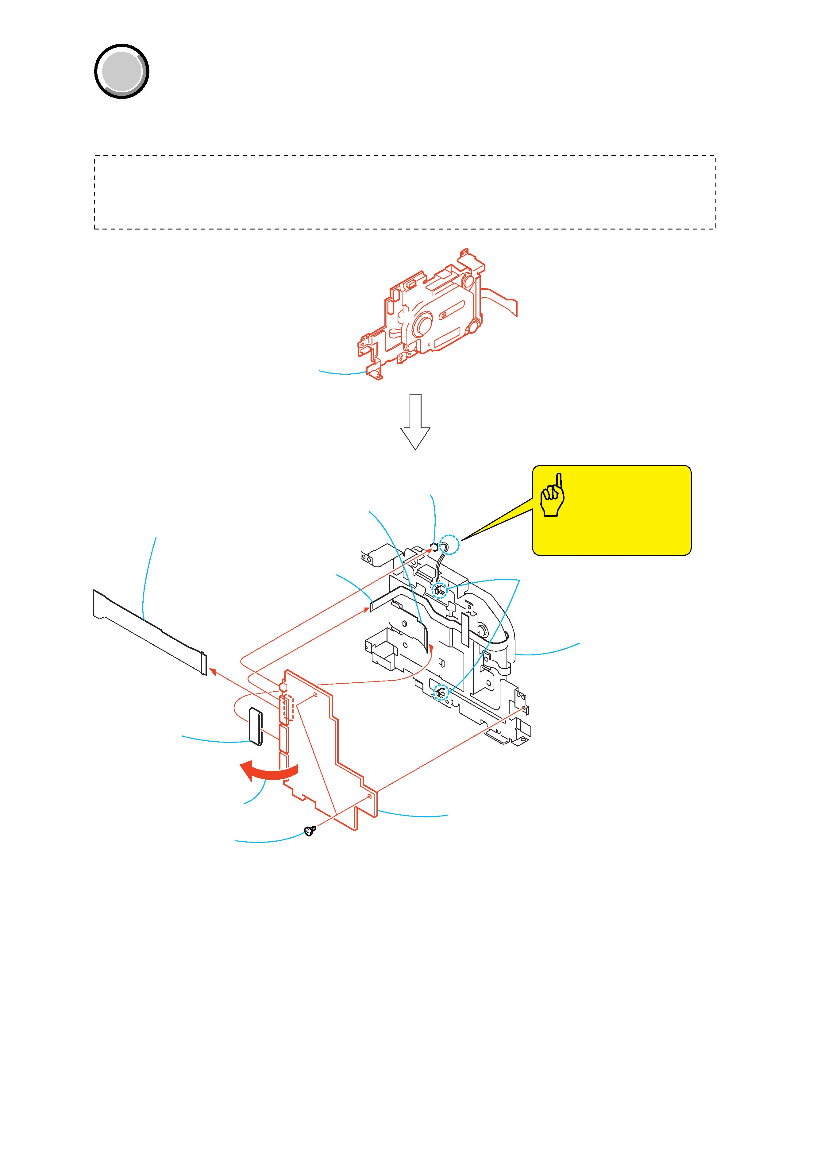
MVC-CD350
COVER
COVER
SY
-087
1
FP-654 flexible board
(39P)
2
FP-656 flexible board (39P)
(from the optical device)
3
Ferrite core
4
Harness DS-117 (2P)
(from the DEW sensor)
Caution
Note: Don't pull at harness of
connector.
6
Two claws
9
SY-087 board
8
Flexible board (15P)
(from the spindle motor)
5
Two screws (M1.7
× 3)
7
Turn over the SY-087 board
in the direction of the arrow.
8
DDX-G3000
complete section
DDX-G3000
complete section,
SY-087 board
Refer to level 2
1
2-3.
SIDE CABINET SECTION...............................
2
2-5.
DISCHARGING THE CAPACITOR..................
3
2-6.
CABINET (REAR) SECTION ..........................
4 2-7.
DDX-G3000 COMPLETE SECTION................
(page 2-4)
(page 2-5)
(page 2-6)
(page 2-7)
Before starting the following disassembling work,
sections 2-3 and 2-5~2-7 must have already been
completed beforehand.
2-18.SY-087 BOARD
NOTE: Follow the disassembly procedure in the numerical order given.
2-18
MVC-CD350
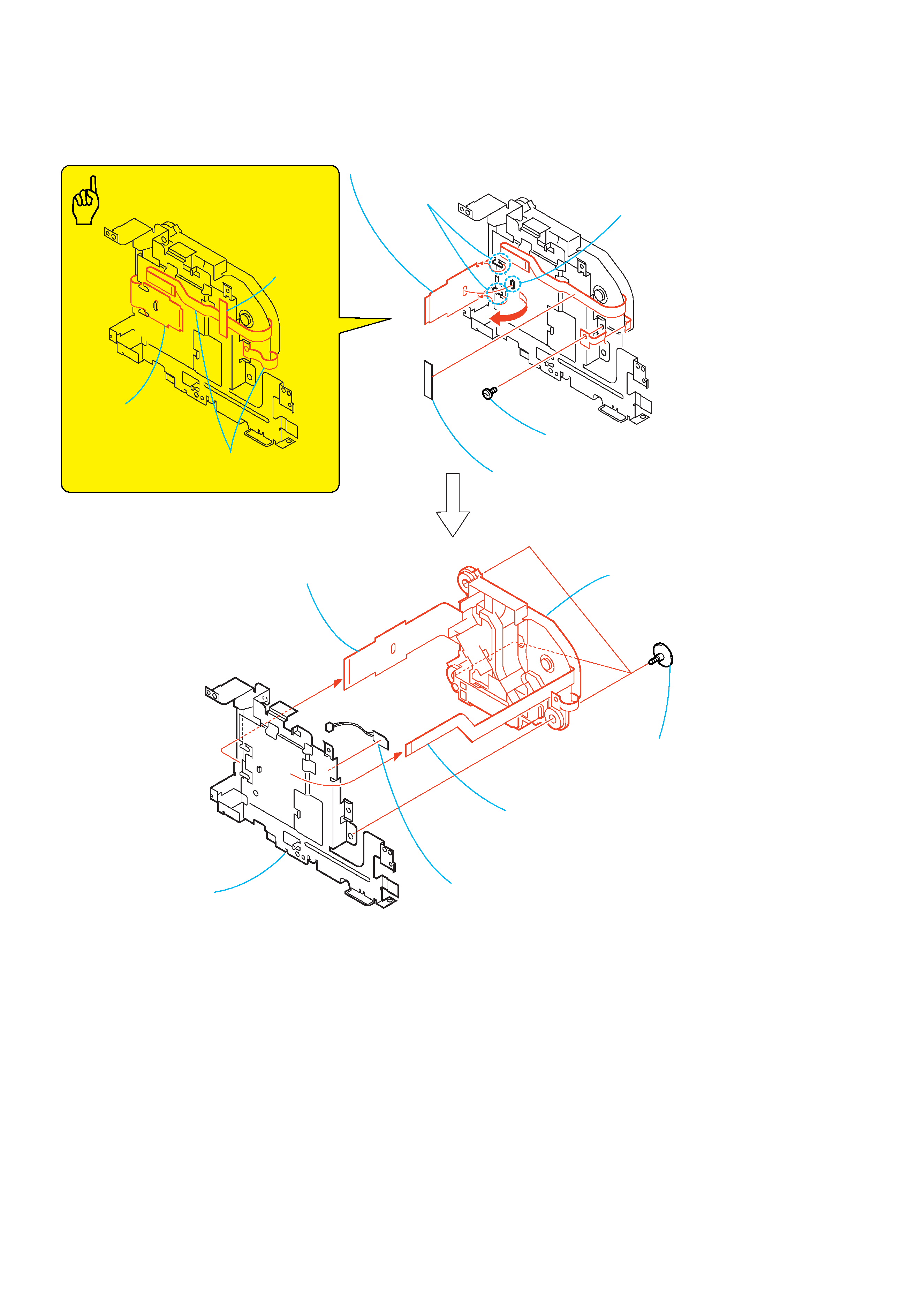
2-19.BU ASSEMBLY
7
FP-248 flexible board,
Harness DS-117
(DEW sensor)
9
BU assembly
8
Main frame
1
Tape (A)
3
Dowel
4
Two claws
5
Remove the FP-656 flexible board
in the direction of the arrow.
Caution
FP-656 flexible board
Tape (A)
Flexible board
(from the spindle motor)
6
Three BU step screws
Flexible board
(from the spindle motor)
FP-656 flexible board
(from the optical device)
2
Screw (M1.7
× 3)