SERVICE MANUAL
Other specifications
Disc player section
MD player
Signal-to-noise ratio
90 dB
Frequency response
10 20,000 Hz
Wow and flutter
Below measurable limit
Laser Diode Properties
Material
GaAlAs
Wavelength
780 nm
Emission Duration
Continuous
Laser output power
Less than 44.6 W*
* This output is the value measured at a distance
of 200 mm from the objective lens surface on
the Optical Pick-up Block.
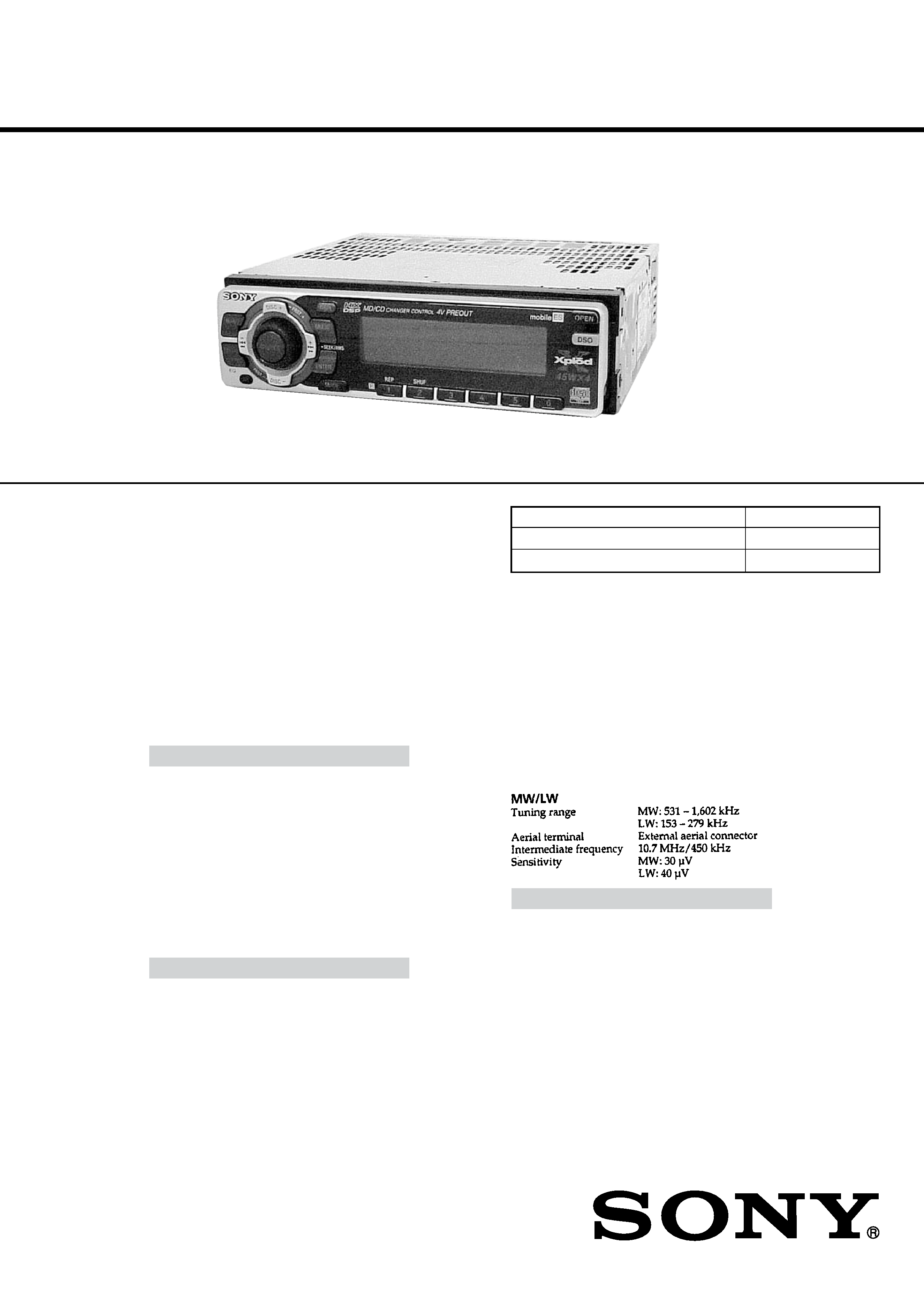
Tuner section
FM
Tuning range
87.5 107.9 MHz
(MDX-C8500X)
87.5 108.0 MHz
(MDX-C8500R)
Antenna terminal
External antenna connector
Intermediate frequency
10.7 MHz/450 kHz
Usable sensitivity
8 dBf
Selectivity
75 dB at 400 kHz
Signal-to-noise ratio
66 dB (stereo),
72 dB (mono)
Harmonic distortion at 1 kHz
0.6 % (stereo),
0.3 % (mono)
Separation
35 dB at 1 kHz
Frequency response
30 15,000 Hz
AM (MDX-C8500X)
Tuning range
530 1,710 kHz
Antenna terminal
External antenna connector
Intermediate frequency
10.7 MHz/450 kHz
Sensitivity
30
µV
Power amplifier section
Outputs
Speaker outputs
(sure seal connectors)
Speaker impedance
4 8 ohms
Maximum power output 50 W
× 4 (at 4 ohms)
AUDIO POWER SPECIFICATIONS (MDX-C8500X)
POWER OUTPUT AND TOTAL HARMONIC DISTORTION
19 watts per channel minimum continuous average power into 4ohms, 4
channels driven from 10 Hz to 20 kHz with no more than 1% total harmonic
distortion.
Model Name Using Similar Mechanism
NEW
Base Mechanism Type
MG-164NV-138
Optical Pick-up Name
KMS-241C
US Model
MDX-C8500X
AEP Model
UK Model
MDX-C8500R
SPECIFICATIONS
MDX-C8500R/C8500X
Photo: MDX-C8500X
FM/AM(MW/LW) MINIDISC PLAYER
Continued on next page
(MDX-C8500R)
Ver 1.2 2002.03
9-870-096-13
Sony Corporation
2002C0500-1
e Vehicle Company
C
2002.03
Published by Sony Engineering Corporation

2
1.
SERVICING NOTES ............................................... 3
2.
GENERAL
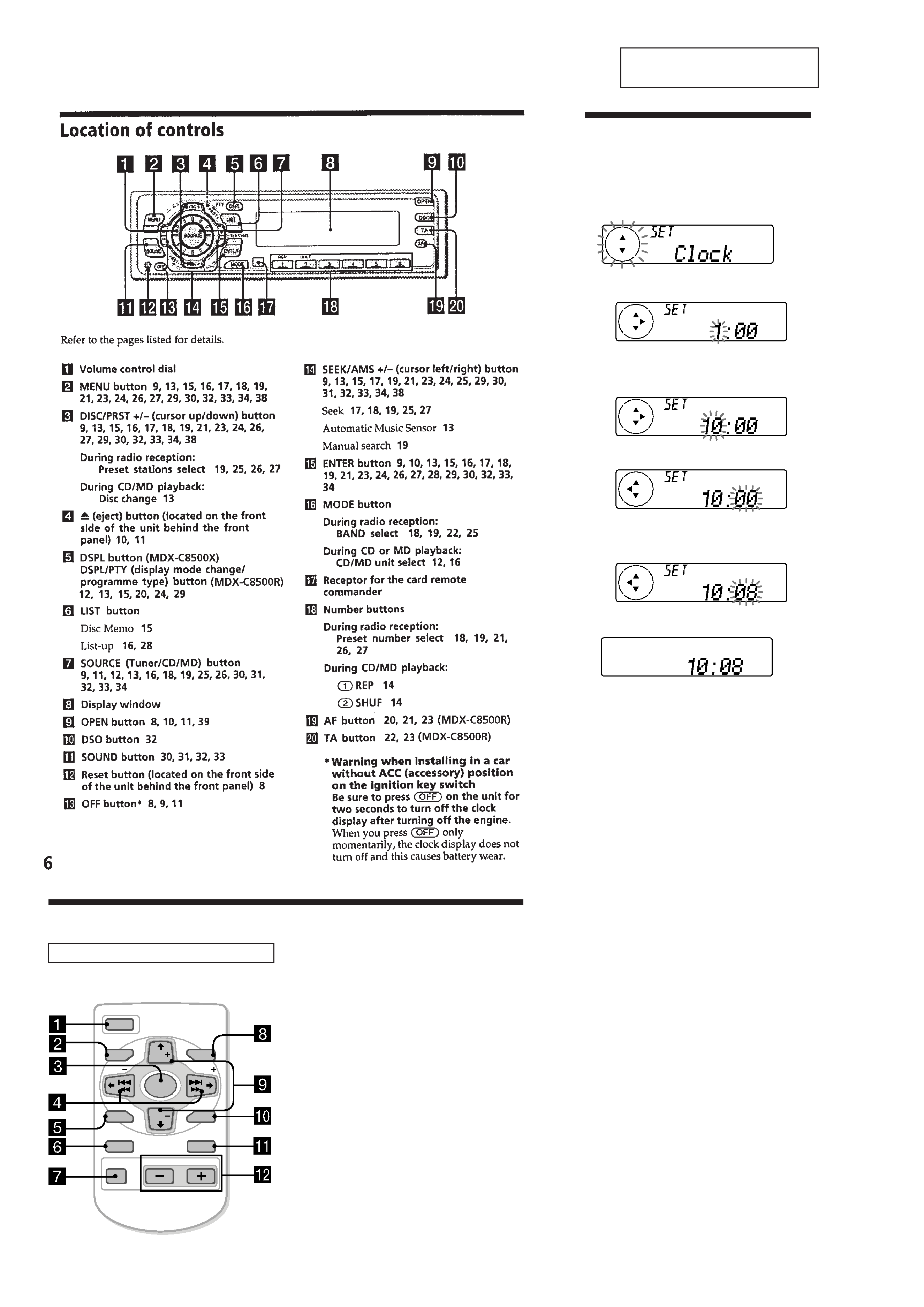
Location of Controls .......................................................
4
Setting the Clock .............................................................
4
Installation .......................................................................
5
Connections .....................................................................
7
3.
DISASSEMBLY ......................................................... 11
4.
ELECTRICAL ADJUSTMENTS
Test Mode ........................................................................ 18
MD Section ..................................................................... 18
Tuner Section .................................................................. 18
5.
DIAGRAMS
5-1. Block Diagram SERVO Section ............................... 19
5-2. Block Diagram TUNER Section .............................. 20
5-3. Block Diagram MAIN Section ................................. 21
5-4. Block Diagram
DISPLAY/KEY CONTROL Section ........................ 22
5-5. Block Diagram
BUS CONTROL/POWER SUPPLY Section ........... 23
5-6. Note for Printed Wiring Boards and
Schematic Diagrams ....................................................... 24
5-7. Printed Wiring Boards
SERVO Board (Component Side)/
SENSOR Board ............................................................ 26
5-8. Printed Wiring Board
SERVO Board (Conductor Side) .............................. 27
5-9. Schematic Diagram
SERVO Board (1/2)/ SENSOR Board ...................... 28
5-10. Schematic Diagram SERVO Board (2/2) ................. 29
5-11. Printed Wiring Board
MAIN Board (Component Side) .............................. 30
5-12. Printed Wiring Board
MAIN Board (Conductor Side) ................................ 31
5-13. Schematic Diagram MAIN Board (1/4) ................... 32
5-14. Schematic Diagram MAIN Board (2/4) ................... 33
5-15. Schematic Diagram MAIN Board (3/4) ................... 34
5-16. Schematic Diagram MAIN Board (4/4) ................... 35
5-17. Printed Wiring Board DSO Board ............................ 36
5-18. Schematic Diagram DSO Board ............................... 37
5-19. Printed Wiring Board SUB Board ............................ 38
5-20. Schematic Diagram SUB Board ............................... 39
5-21. Printed Wiring Board KEY Board ............................ 40
5.22. Schematic Diagram KEY Board .............................. 41
5-23. IC Pin Function Description ........................................... 47
6.
EXPLODED VIEWS ................................................ 59
7.
ELECTRICAL PARTS LIST ............................... 63
TABLE OF CONTENTS
General
Outputs
Audio outputs
Power antenna relay
control lead
Power amplifier control
lead
Telephone ATT control
lead
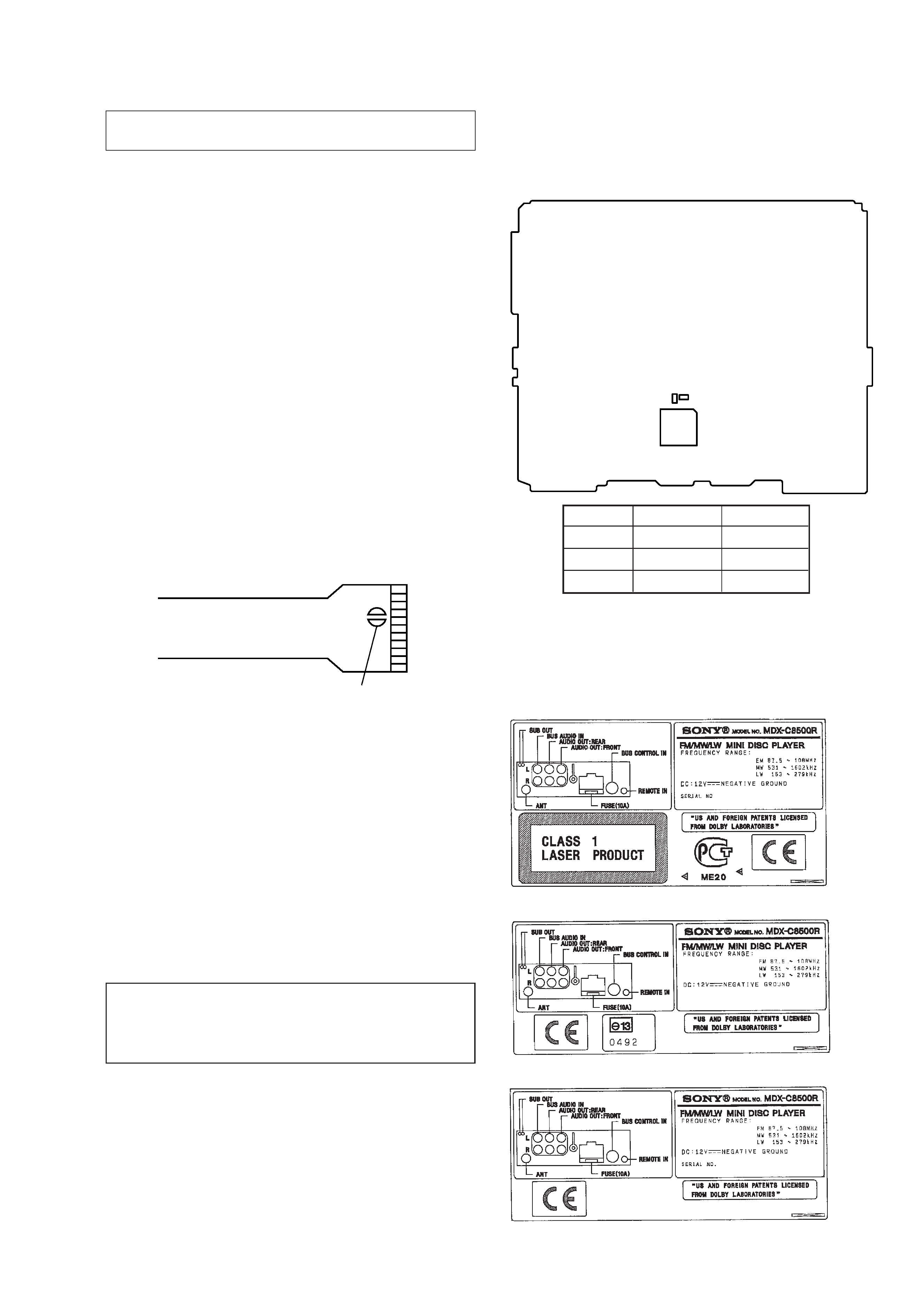
Power requirements
12 V DC car battery
(negative ground)
Dimensions
Approx. 178
× 50 × 183 mm
(7 1/8
× 2 × 7 1/8 in.)
(w/h/d)
Mounting dimensions
Approx. 182
× 53 × 162 mm
(7 1/4
× 2 1/8 × 6 3/8 in.)
(w/h/d)
Mass
Approx. 1.2 kg (2 lb 10 oz)
Supplied accessories
Card remote commander
RM-X91 (MDX-C8500X)
Parts for installation and
connections (1 set)
Front panel case (1)
U.S. and foreign patents licensed from Dolby
laboratories Licensing Corporation.
Design and specifications are subject to change
without notice.
3
SAFETY-RELATED COMPONENT WARNING!!
COMPONENTS IDENTIFIED BY MARK 0 OR DOTTED
LINE WITH MARK 0 ON THE SCHEMATIC DIAGRAMS
AND IN THE PARTS LIST ARE CRITICAL TO SAFE
OPERATION. REPLACE THESE COMPONENTS WITH
SONY PARTS WHOSE PART NUMBERS APPEAR AS
SHOWN IN THIS MANUAL OR IN SUPPLEMENTS PUB-
LISHED BY SONY.
SECTION 1
SERVICING NOTES
· Model Identification
There are three types of main board in according of destination
for MDX-C8500R.
MAIN BOARD (Component Side)
Notes on chip component replacement
· Never reuse a disconnected chip component.
· Notice that the minus side of a tantalum capacitor may be dam-
aged by heat.
Flexible Circuit Board Repairing
· Keep the temperature of the soldering iron around 270 °C dur-
ing repairing.
· Do not touch the soldering iron on the same conductor of the
circuit board (within 3 times).
· Be careful not to apply force on the conductor when soldering
or unsoldering.
NOTES ON HANDLING THE OPTICAL PICK-UP
BLOCK OR BASE UNIT
CAUTION
Use of controls or adjustments or performance of procedures
other than those specified herein may result in hazardous ra-
diation exposure.
The laser diode in the optical pick-up block may suffer electro-
static break-down because of the potential difference generated
by the charged electrostatic load, etc. on clothing and the human
body.
During repair, pay attention to electrostatic break-down and also
use the procedure in the printed matter which is included in the
repair parts.
The flexible board is easily damaged and should be handled with
care.
NOTES ON LASER DIODE EMISSION CHECK
Never look into the laser diode emission from right avove when
checking it for adustment. It is feared that you will lose your sight.
NOTES ON HANDLING THE OPTICAL PICK-UP BLOCK
(KMS-241C/J1NP)
The laser diode in the optical pick-up block may suffer electro-
static break-down easily. When handling it, perform soldering
bridge to the laser-tap on the flexible board. Also perform m easures
against electrostatic break-down sufficiently before the operation.
The flexible board is easily damaged and should be handled with
care.
laser-tap
OPTICAL PICK-UP FLEXIBLE BOARD
R502
R503
IC502
R502
R503
TYPE A
a
×
TYPE B
×
a
TYPE C
aa
Type A, B and C can be identified by its model number label at
the buttom of the set.
SPECIFICATION LABEL
TYPE A
TYPE B
TYPE C
4
SECTION 2
GENERAL
This section is extracted from
instruction manual.
Setting the clock
The clock uses a 12-hour digital indication.
Example: To set the clock to 10:08
1 Press (MENU), then press either side of
(DISC/PRST)
repeatedly until "Clock"
appears.
1
Press (ENTER).
The hour indication flashes.
2
Press either side of (DISC/PRST) to set
the hour.
3
Press (+) side of (SEEK/AMS).
The minute indication flashes.
4
Press either side of (DISC/PRST) to set
the minute.
2 Press (ENTER).
The clock starts.
After the clock setting is completed, the
display returns to normal playback mode.
Tip
You can set the clock automatically with the RDS
feature (see page 24). (MDX-C8500R)
Note
In the initial setting, the clock indication appears
while the unit is turned off.
When you select the "on" setting of the "D.Info"
item (page 29), you can see the clock indication in
the upper part of the display while you are
enjoying any source.
Location of controls (MDX-C8500X)
Card remote commander RM-X91
The corresponding buttons of the card
remote commander control the same
functions as those on this unit.
1 OFF button
2 MENU button
3 SOURCE button
4 SEEK/AMS (cursor </,) buttons
5 SOUND button
6 DSPL button
7 ATT button
8 LIST button
9 DISC/PRST (cursor M/m) buttons
0 ENTER button
qa MODE button
qs VOL buttons
OFF
SEEK
SEEK
OPEN/CLOSE
MENU
LIST
SOUND
ENTER
DSPL
MODE
VOL
ATT
DISC
DISC
SOURCE
5