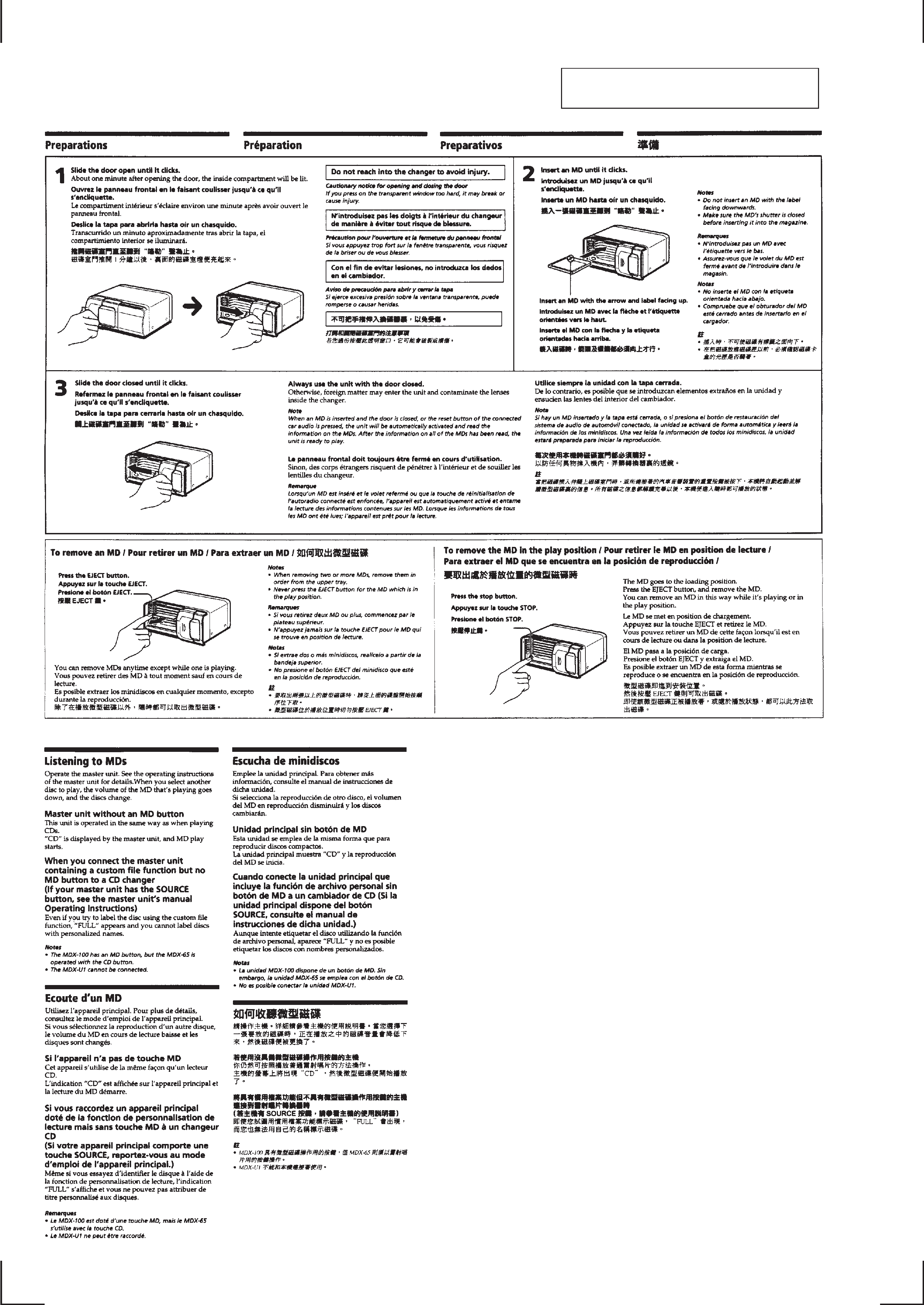
1
MICROFILM
Model Name Using Similar Mechanism
MDX-62
Mini Disc Mechanism Type
MG-798K-133
Optical Pick-up Name
KMS-241A/J2N
SERVICE MANUAL
US Model
Canadian Model
AEP Model
UK Model
E Model
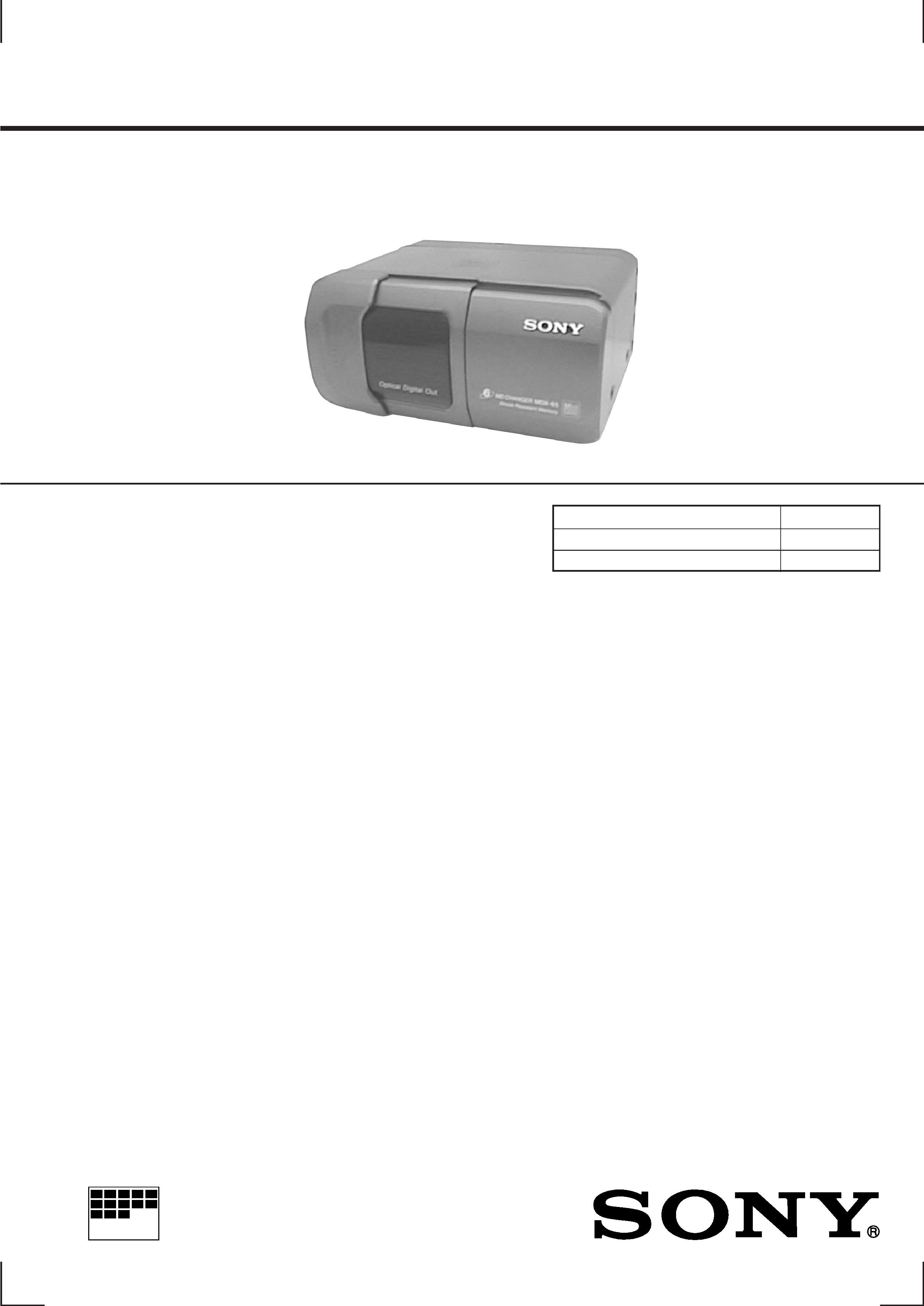
MDX-65
MINIDISC CHANGER
System
Mini disc digital audio system
Laser Diode Properties
Material: GaAlAs
Wavelength: 780 nm
Emission Duration: Continuous
Laser output Power: Less than
44.6
µW*
* This output is the value measured at a distance of
200 mm from the objective lens surface on the
Optical Pick-up Block.
Frequency response
10 20,000 Hz
Wow and flutter Below measurable limit
Signal-to-noise ratio
95 dB
Outputs
Bus control output (8 PIN)
Analog audio output (RCA PIN)
Current drain
300 mA (MD playback)
600 mA (during loading or ejecting a
disc)
Dimensions
Approx. 176
× 83.5 × 142 mm
(7
× 3 3/8 × 5 18/32 in.) (w/h/d) not incl.
projecting parts and controls
Mass
Approx. 1.1 kg (2 lb. 7 oz.)
Power requirement
12 V DC car battery (negative
ground)
Supplied accessories
Mounting hardware (1 set)
Bus cable 5.5 m (1)
RCA pin cord 5.5 m (1)
· U.S. and foreign patents licensed from Dolby
Laboratories Licensing Corporation.
· Design and specifications subject to change without
notice.
SPECIFICATIONS
· Sony BUS system compatible with mobile MD
changers.
· Direct-in system for inserting and removing
MDs easily.
· No waiting time to change discs in continuous
play.
· The MD changer compartment has a built in light
for easy use even in the dark.
· 1 bit Digital/Analog converter for high quality
sound reproduction.
FEATURES
Dolby noise reduction extension manufactured under license
from Dolby Laboratories Licensing Corporation.
"DOLBY" and the double-D symbol
a are trademarks of Dolby
Laboratories Licensing Corporation.
2
TABLE OF CONTENTS
1. SERVICE NOTE
1-1. To Place the Set into Playback Mode ................................. 3
1-2. How to Check the Servo Board Waveforms ...................... 3
2. GENERAL
Preparations ............................................................................ 4
Listening MDs ........................................................................ 4
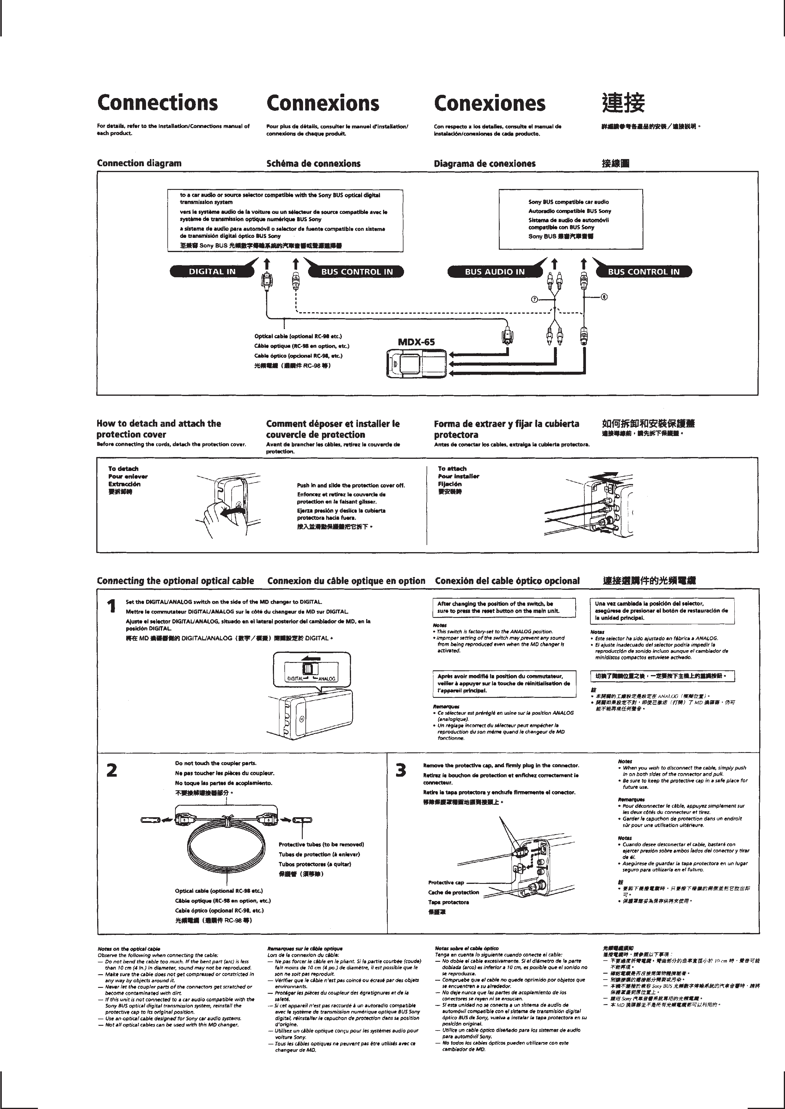
Connections ............................................................................ 5
3. DISASSEMBLY
3-1. Panel (Rear) Assy ............................................................... 6
3-2. Case (Upper) ...................................................................... 6
3-3. Panel (Front) Assy .............................................................. 7
3-4. MD Block ........................................................................... 7
3-5. Main Board ........................................................................ 8
3-6. Chassis (OP) Block ............................................................ 8
3-7. Servo Board ........................................................................ 9
3-8. Optical Pick-up .................................................................. 9
3-9. Note on Assembly for the Chassis (OP) Block ................ 10
4. DIAGRAMS
4-1. IC Pin Descriptions .......................................................... 11
4-2. Circuit Boards Location ................................................... 14
4-3. Block Diagram ................................................................. 15
4-4. Printed Wiring Boards Servo Section .......................... 17
4-5. Schematic Diagram Servo Section ............................... 21
4-6. Schematic Diagram Main Section ................................ 23
4-7. Printed Wiring Boards Main Section ........................... 26
4-8. Printed Wiring Board Power Section ........................... 29
4-9. Schematic Diagram Power Section .............................. 31
5. EXPLODED VIEWS
5-1. Case Section ..................................................................... 38
5-2. Main Board Section ......................................................... 39
5-3. MD Section (1) ................................................................. 40
5-4. MD Section (2) ................................................................. 41
5-5. MD Section (3) ................................................................. 42
6. ELECTRICAL PARTS LIST ....................................... 43
SERVICE NOTE
CAUTION
Use of controls or adjustments or performance of proce-
dures other than those specified herein may result in haz-
ardous radiation exposure.
Notes on Chip Component Replacement
· Never reuse a disconnected chip component.
· Notice that the minus side of a tantalum capacitor may be dam-
aged by heat.
NOTES ON HANDLINGTHE OPTICAL PICK-UP BLOCK OR
BASE UNIT
The laser diode in the optical pick-up block may suffer electrostatic
breakdown because of the potential difference generated by the
charged electrostatic load, etc. on clothing and the human body.
During repair, pay attention to electrostatic breakdown and also use
the procedure in the printed matter which is included in the repair
parts.
The flexible board is easily damaged and should be handled with
care.
NOTES ON LASER DIODE EMISSION CHECK
The laser beam on this model is concentrated so as to be focused on
the disc reflective surface by the objective lens in the optical pick-up
block. Therefore, when checking the laser diode emission, observe
from more than 30 cm away from the objective lens.
NOTES ON PICK-UP FLEXIBLE BOARD
The pick-up flexible board in this set is secured to the optical pick-up
with an adhesive tape. Once the tape is removed, an adhering force
becomes weak, and it cannot be reused.
Therefore, if the optical pick-up is replaced, replace also the pick-up
flexible board with a new one.
NOTES ON HANDLING THE OPTICAL PICK-UP BLOCK
(KMS-241A/J2N)
The laser diode in the optical pick-up block may suffer electrostatic
break-down easily. When handling it, perform soldering bridge to
the laser-tap on the flexible board. Also perform measures against
electrostatic break-down sufficiently before the operation. The
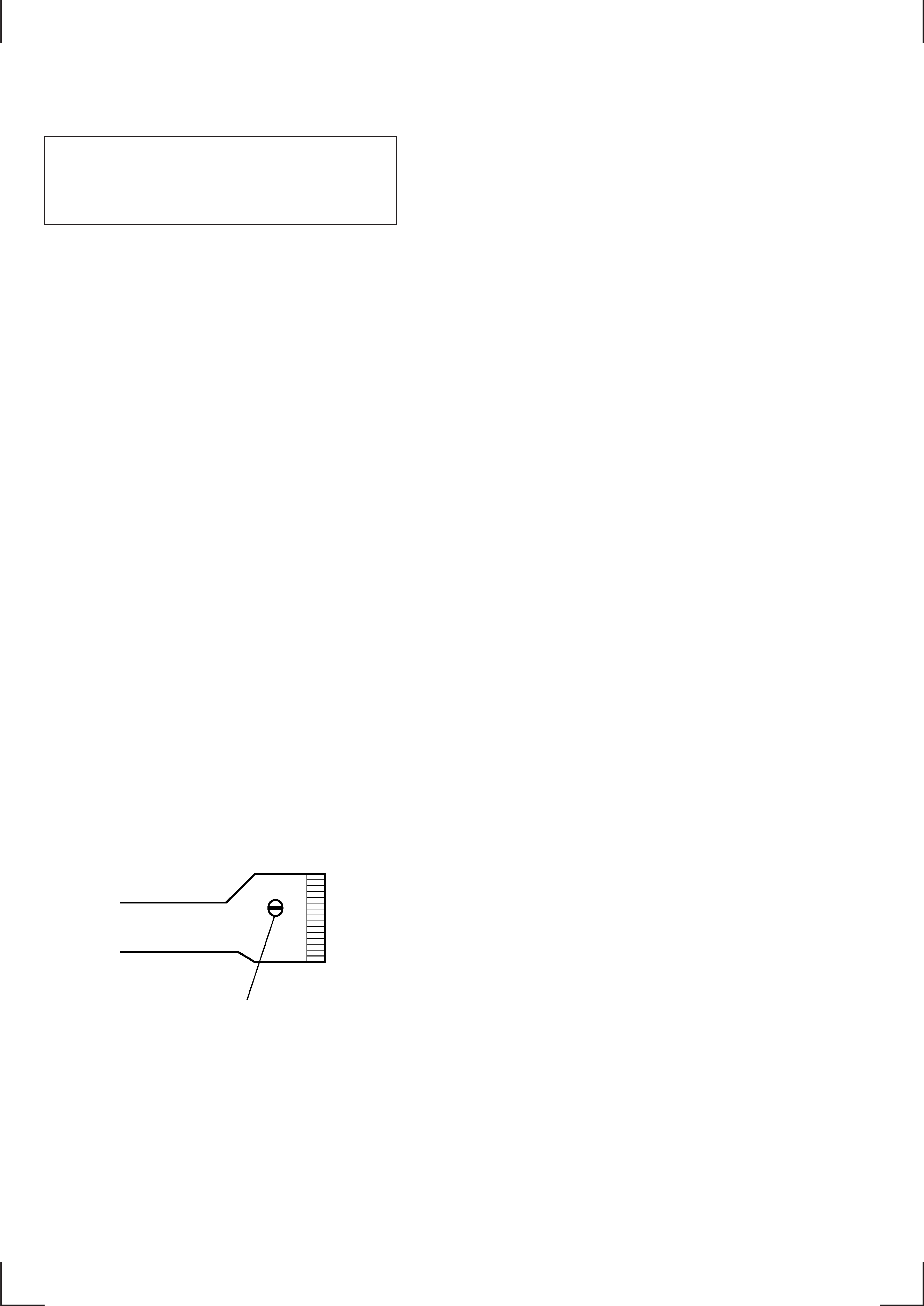
flexible board is easily damaged and should be handled with care.
laser-tap
SAFETY-RELATED COMPONENT WARNING!!
COMPONENTS IDENTIFIED BY MARK
! OR DOTTED LINE
WITH MARK
! ON THE SCHEMATIC DIAGRAMS AND IN
THE PARTS LIST ARE CRITICAL TO SAFE OPERATION.
REPLACE THESE COMPONENTS WITH SONY PARTS WHOSE
PART NUMBERS APPEAR AS SHOWN IN THIS MANUAL OR
IN SUPPLEMENTS PUBLISHED BY SONY.
OPTICAL PICK-UP FLEXIBLE BOARD
ATTENTION AU COMPOSANT AYANT RAPPORT
À LA SÉCURITÉ!!
LES COMPOSANTS IDENTIFIÉS PAR UNE MARQUE
! SUR LES
DIAGRAMMES SCHÉMATIQUES ET LA LISTE DES PIÈCES SONT
CRITIQUES POUR LA SÉCURITÉ DE FONCTIONNEMENT. NE
REMPLACER CES COMPOSANTS QUE PAR DES PIÈCES SONY
DONT LES NUMÉROS SONT DONNÉS DANS CE MANUEL OU
DANS LES SUPPLÉMENTS PUBLIÉS PAR SONY.
3
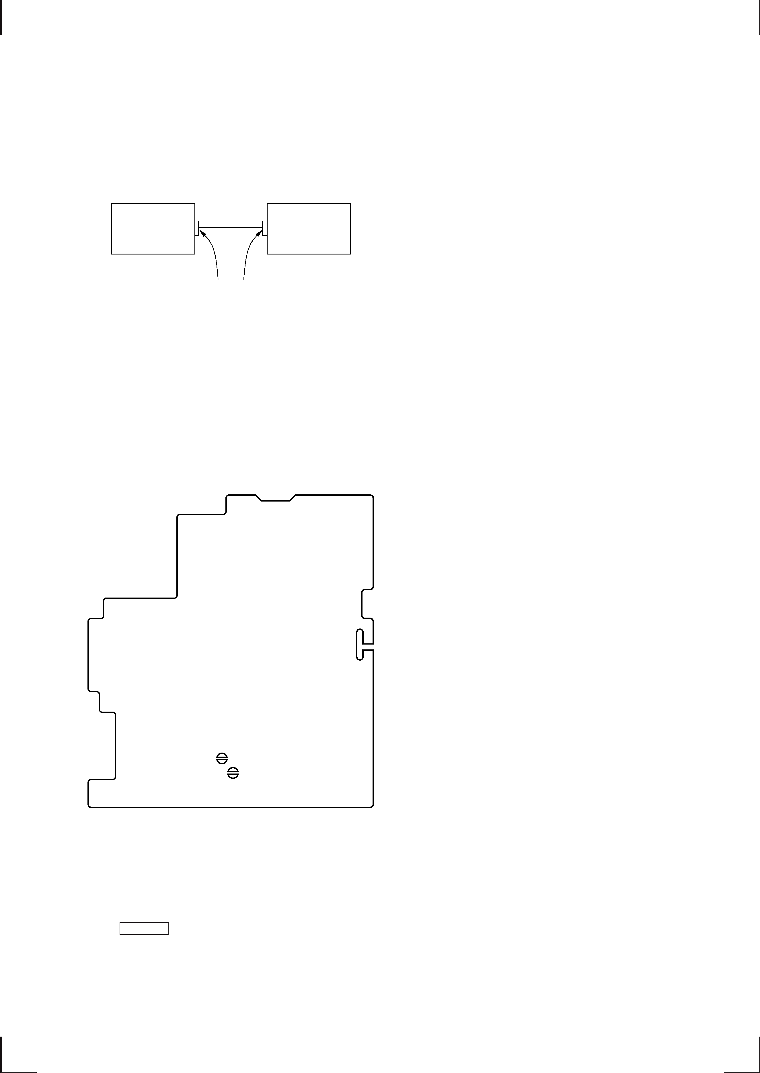
BP1
BP2
MDX-65
Master unit
(CDX-C880,
C880R, etc.)
BUS CONTROL IN
BUS CONTROL OUT
SECTION 1
SERVICE NOTE
1-1. TO PLACE THE SET INTO PLAYBACK MODE
The this set has no key control function and cannot be placed into
the Playback mode alone.
For key control, the this set is controlled through serial
communication with a master unit (car audio player, TV tuner or
source selector compatible with the Sony BUS system.)
To service the this set, the set should be connected as given below:
1-2. HOW TO CHECK THE SERVO BOARD
WAVEFORMS
1. Remove the panel (rear) assy, case (upper) and panel (front) assy.
Then, remove the main board from the mechanism deck. (See
page 8 of "SECTION 3. DISASSEMBLY".)
2. Remove the chassis (OP) block from the mechanism deck. (See
page 10 of "SECTION 3. DISASSEMBLY".)
3. Short each bridge points BP1 and BP2 on the main board by
solder bridge.
main board (conductor side)
4. Connect the power board with the main board by the main
flexible board. Connect the main board with the servo board by
the servo flexible board.
5. Connect to a master unit. With the master unit OFF, press the
preset buttons 4
n 5 n 1 (2 seconds or more each) in this
turn to enter the TEST mode.
6. Open the doors and insert a disc in the chassis (OP) assy. Use
the SOURCE button on the master unit to select to MD to
playback.
7. Check the waveforms at each point on the servo board.
Note: After this check is completed, remove solder between
shorted bridge points BP1 and BP2 and open these points.
4
SECTION 2
GENERAL
This section extracted from US,
Canadian, E model's instruction manual.
5