MODEL
COMMANDER DEST.
CHASSIS NO.
KV-T25SN81 RM-870 New Zealand SCC-K37F-A
SERVICE MANUAL
MODEL
COMMANDER DEST. CHASSIS NO.
CHASSIS
TRINITRON ® COLOR TV
BG-1S
2
KV-T25SN81
RM-870
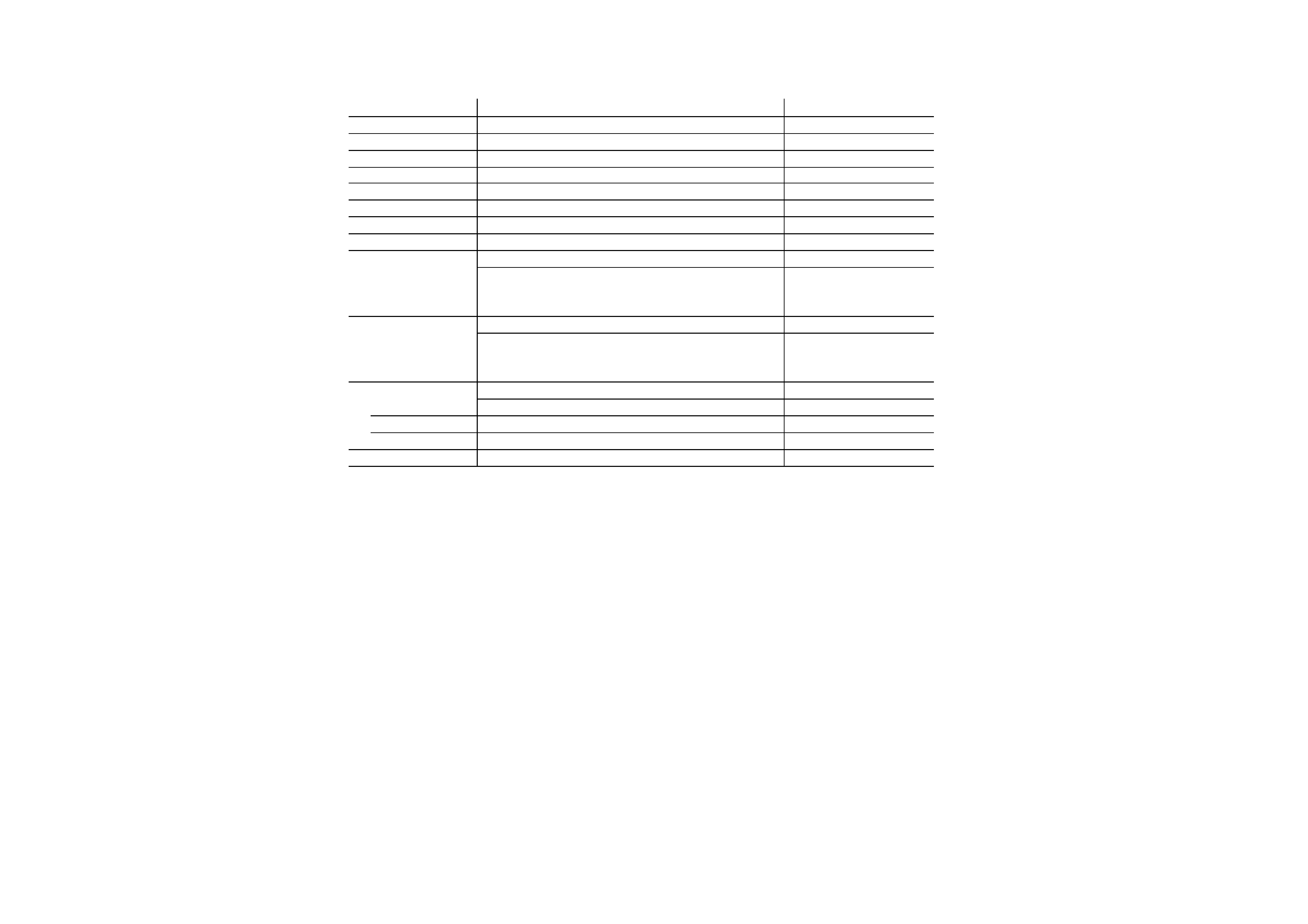
SPECIFICATIONS
Note
Power requirements
110-240 V AC, 50/60 Hz
Power consumption (W) Indicated on the rear of the TV
Television system
B/G
Color system
PAL, PAL 60, NTSC4.43, NTSC3.58(AV IN)
Stereo/Bilingual system
NICAM Stereo/Bilingual B/G, A2 Stereo/Bilingual (German) B/G
Teletext Language
English, German, Swedish, Italian, French, Spanish
Channel coverage
VHF : 1 to 11 / UHF : 21 to 69 / CATV: S01 to S03, S1 to S41
Audio output (speaker)
5W
× 2
Inputs
Antenna: 75 ohms
VIDEO IN jacks: phono jacks
Video: 1 Vp-p, 75 ohms
Audio: 500 mVrms, high impedance
Outputs
Headphone jack: minijack
MONITOR OUT jacks: phono jacks
Video: 1 Vp-p, 75 ohms
Audio: 500 mVrms
Picture tube
25 in.
Tube size (cm)
64
Measured diagonally
Screen size (cm)
60
Measured diagonally
Dimensions (w/h/d, mm)
613
× 542 × 472
Mass (kg)
32
Design and specifications are subject to change without notice.
CAUTION
SHORT CIRCUIT THE ANODE OF THE PICTURE TUBE AND
THE ANODE CAP TO THE METAL CHASSIS, CRT SHIELD, OR
CARBON PAINTED ON THE CRT, AFTER REMOVING THE
ANODE.
SAFETY-RELATED COMPONENT WARNING!!
COMPONENTS IDENTIFIED BY SHADING AND MARK ! ON
THE SCHEMATIC DIAGRAMS, EXPLODED VIEWS AND IN THE
PARTS LIST ARE CRITICAL TO SAFE OPERATION. REPLACE
THESE COMPONENTS WITH SONY PARTS WHOSE PART
NUMBERS APPEAR AS SHOWN IN THIS MANUAL OR IN
SUPPLEMENTS PUBLISHED BY SONY.

3
KV-T25SN81
RM-870
TABLE OF CONTENTS
SELF DIAGNOSIS FUNCTION ...............................
4
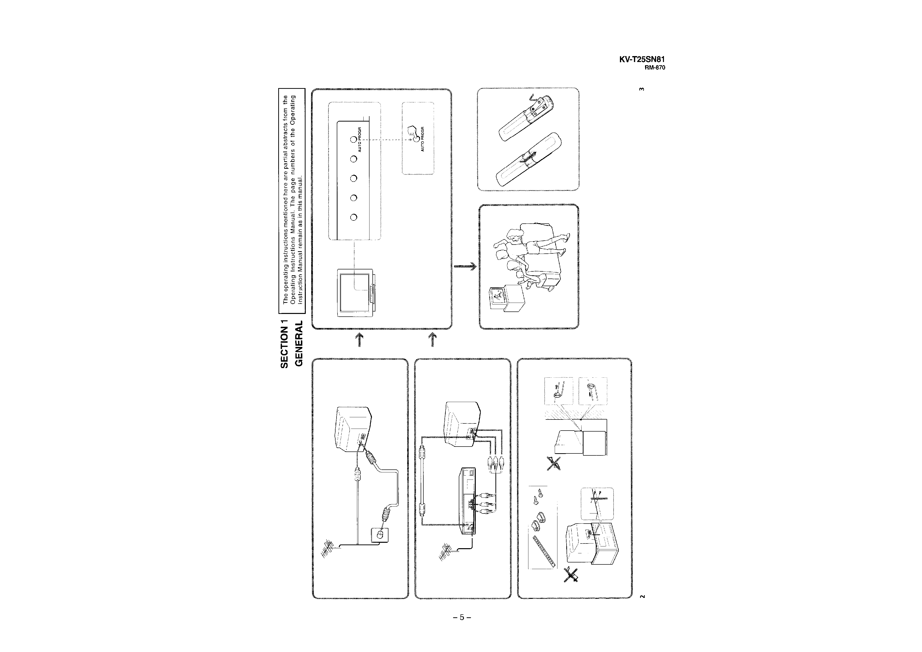
1. GENERAL ....................................................................
5
2. DISASSEMBLY
2-1.
Rear Cover Removal ............................................
11
2-2.
A Board Removal ................................................
11
2-3.
F1 Board Removal ...............................................
11
2-4.
Service Position ...................................................
11
2-5.
Replacement of Parts ...........................................
12
2-6.
Demagnetization Coil Removal ..........................
12
2-7.
Picture Tube Removal ..........................................
13
3. SET-UP ADJUSTMENTS
3-1.
Beam Landing ......................................................
14
3-2.
Convergence .........................................................
15
3-3.
Focus Adjustment ................................................
17
3-4.
G2 (Screen) and White Balance Adjustments .....
17
4. CIRCUIT ADJUSTMENTS
4-1.
Adjustments with Commander ............................
18
4-2.
Adjustment Method .............................................
19
4-3.
A Board Adjustment after IC003 (Memory)
Replacement.........................................................
22
4-4.
Picture Distortion Adjustment .............................
22
5. DIAGRAMS
5-1.
Block Diagram ......................................................
25
5-2.
Circuit Boards Location .......................................
29
5-3.
Schematic Diagrams and Printed Wiring Boards.
29
(1)
Schematic Diagram of A Board ...........................
33
(2)
Schematic Diagrams of A3, F1 and V1 Boards ...
37
(3)
Schematic Diagrams of C and VM Boards ..........
45
5-4.
Semiconductors .....................................................
48
6. EXPLODED VIEW
6-1.
Chassis ..................................................................
51
7. ELECTRICAL PARTS LIST ...................................
53
Section
Title
Page
Section
Title
Page
4
KV-T25SN81
RM-870
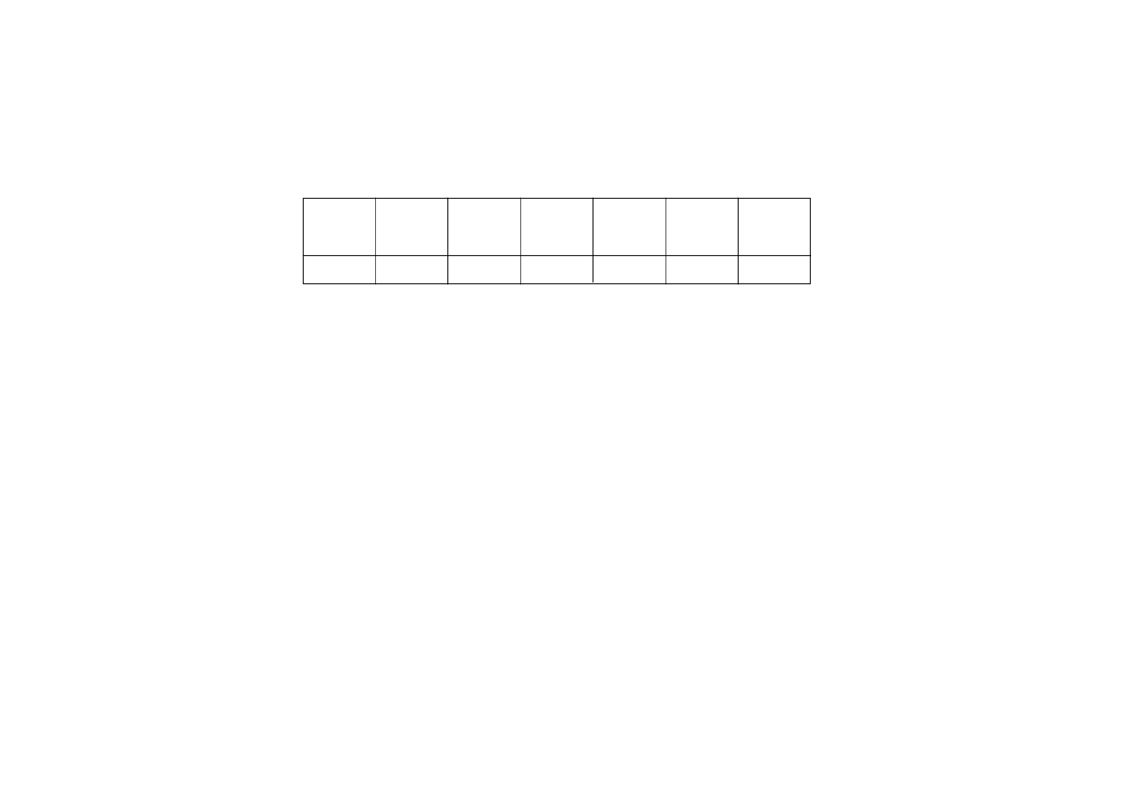
SELF DIAGNOSIS FUNCTION
If no acknowledgement is returned from a device which is turned "ON", the device has a problem.
In this case, one of the LED's responding to the problem device will flicker a defined number of times.
Flickering is operated by lighting the LED's for 60ss each time.
The flickering frequency responding to each failed device is shown below.
All the devices are checked one after another from the left of the table.
If an error is found, the responding LED will start flickering.
So, if more than 1 device have failed, only the one on the left side will flicker.
Device
Flickering
Frequency
NONVOLATILE
MEMORY
1
--
--
Y/C JUNGLE
(IC300)
3
--
--
--
--
TONE
CONTROL
(IC201)
6