MODEL
COMMANDER DEST. CHASSIS NO.
CHASSIS
TRINITRON ® COLOR TV
SERVICE MANUAL
AG3E
MODEL
COMMANDER DEST.
CHASSIS NO.
KV-DR34M69 RM-991 GE
SCC-U84B-A
KV-DR34M69 RM-991 Thailand
SCC-U82B-A
KV-DR34M89 RM-991 ME
SCC-U43C-A

2
KV-DR34M69/DR34M89
RM-991
Power requirements
110-240V AC, 50/60 Hz
KV-DR34M69(GE)/DR34M89
220-240V AC, 50/60 Hz
KV-DR34M69(Thailand)
Power consumption (W)
Indicated on the rear of the TV
Television system
B/G, I, D/K, M
Color system
PAL, PAL 60, SECAM, NTSC3.58, NTSC4.43
Stereo/Bilingual system
NICAM Stereo/Bilingual B/G, I;
KV-DR34M69(Thailand/GE)
A2 Stereo/Bilingual B/G
Teletext language
English, Arabic, French
Channel coverage
B/G
VHF: E2 to E12
UHF: E21 to E69
CATV: S01 to S03, S1 to S41
I
UHF: B21 to B68
CATV: S01 to S03, S1 to S41
D/K
VHF: C1 to C12, R1 to R12
UHF: C13 to C57, R21 to R60
CATV: S01 to S03, S1 to S41, Z1 to Z39
M
VHF: A2 to A13
UHF: A14 to A79
CATV: A-8 to A-2, A to W+4, W+6 to W+84
8
(Antenna)
75-ohm external terminal
Audio output (Speaker)
6W + 6W
3D WOOFER
15W
Number of terminal
DVideo
Input: 4
Output: 1
Phone jacks; 1 Vp-p, 75 ohms
9 Audio
Input: 4
Output: 1
Phone jacks; 500 mVrms
(S Video)
Input : 2
Y: 1 Vp-p, 75 ohms
unbalanced, sync negative
C: 0.286 Vp-p, 75 ohms
(Component
Input : 1
Phono jacks:
Video)
Y: 1 Vp-p, 75 ohms
sync negative
PB/CB: 0.7 Vp-p, 75 ohms
PR/CR: 0.7 Vp-p, 75 ohms
Audio: 500mVrms
2 (Headphone)
Output: 1
Stereo minijack
Picture tube
34 in
Tube size (cm)
86
Measured diagonally
Screen size (cm)
80
Measured diagonally
Dimension (w/h/d,mm)
894
× 690 × 569
Mass (kg)
85
Design and specifications are subject to change without notice.
SPECIFICATIONS
SAFETY-RELATED COMPONENT WARNING!!
COMPONENTS IDENTIFIED BY SHADING AND MARK
! ON
THE SCHEMATIC DIAGRAMS, EXPLODED VIEWS AND IN
THE PARTS LIST ARE CRITICAL TO SAFE OPERATION.
REPLACE THESE COMPONENTS WITH SONY PARTS
WHOSE PART NUMBERS APPEAR AS SHOWN IN THIS
MANUAL OR IN SUPPLEMENTS PUBLISHED BY SONY.
CAUTION
SHORT CIRCUIT THE ANODE OF THE PICTURE TUBE AND
THE ANODE CAP TO THE METAL CHASSIS, CRT SHIELD,
OR CARBON PAINTED ON THE CRT, AFTER REMOVING THE
ANODE.
Note

3
KV-DR34M69/DR34M89
RM-991
TABLE OF CONTENTS
SELF DIAGNOSTIC FUNCTION ....................................... 4
1. DISASSEMBLY
1-1.
Rear Cover Removal .................................................. 7
1-2.
3D Speaker Box Removal .......................................... 7
1-3.
Speaker Removal ........................................................ 7
1-4.
Chassis Assy Removal ................................................ 7
1-5.
DH Board Removal .................................................... 7
1-6.
Service Position .......................................................... 7
1-7
Service Position on TV Stand .................................... 8
1-8.
Terminal Bracket Removal ......................................... 8
1-9.
B3 and D5 Boards Removal ....................................... 8
1-10. F1 Board Removal ...................................................... 8
1-11. BC1 and P Boards Removal ....................................... 8
1-12. H1 and H2 Boards Removal ....................................... 9
1-13. A and D Boards Removal ........................................... 9
1-14. Picture Tube Removal ................................................ 9
2. SERVICE JIG .............................................................. 11
3. CIRCUIT BOARDS LOCATION ................................. 11
4. ADVANCE OPERATION
4-1.
"RESET" Function ................................................... 12
5. SET-UP ADJUSTMENTS
5-1.
Beam Landing .......................................................... 13
5-2.
Convergence Adjustment ......................................... 14
5-3.
Focus Adjustment ..................................................... 16
5-4.
Neck Assy Twist Adjustment ................................... 16
5-5.
G2 (SCREEN) and White Balance Adjustment ....... 16
6. CIRCUIT ADJUSTMENTS
6-1.
Adjustment With Commander ................................. 17
6-2.
Adjustment Method .................................................. 17
6-3.
Picture Quality Adjustments .................................... 36
6-4.
Sub Hue/Col Adjustments ........................................ 36
6-5.
Deflection Adjustments ............................................ 37
6-6.
A Board Adjustment After IC003 (MEMORY)
Replacement ............................................................. 38
6-7.
Picture Distortion Adjustment .................................. 39
Section
Title
Page
Section
Title
Page
7. DIAGRAMS
7-1.
Block Diagram ......................................................... 40
7-2.
Schematic Diagram .................................................. 49
(1) A Board Schematic Diagrams ............................ 50
(2) B3 Board Schematic Diagram ............................ 54
(3) D Board Schematic Diagram .............................. 56
(4) D5 Board Schematic Diagram ........................... 58
(5) C Board Schematic Diagram .............................. 60
(6) P and F1 Boards Schematic Diagrams ............... 62
(7) BC1 Board Schematic Diagram ......................... 64
(8) H1 Board Schematic Diagram ........................... 66
(9) V2 Board Schematics Diagram .......................... 68
(10) DH and VM Boards Schematics Diagrams ........ 70
(11) H2 and J Boards Schematic Diagrams ............. 72
7-3.
Voltage Measurement and Waveforms ..................... 76
7-4.
Printed Wiring Boards and Parts Location .............. 90
7-5.
Semiconductors ...................................................... 102
8. EXPLODED VIEWS
8-1.
Speaker Bracket ...................................................... 105
8-2.
3D Speaker ............................................................. 105
8-3.
Chassis .................................................................... 106
8-4.
Picture Tube ............................................................ 108
9. ELECTRICAL PARTS LIST ...................................... 109
OPERATING INSTRUCTIONS
4
KV-DR34M69/DR34M89
RM-991
The units in this manual contain a self-diagnostic function. If an error occurs, the STANDBY/TIMER lamp will automatically
begin to flash.
The number of times the lamp flashes translates to a probable source of the problem. A definition of the STANDBY/TIMER
lamp flash indicators is listed in the instruction manual for the user's knowledge and reference. If an error symptom cannot
be reproduced, the remote commander can be used to review the failure occurrence data stored in memory to reveal past
problems and how often these problems occur.
1.
DIAGNOSTIC TEST INDICATORS
When an error occurs, the STANDBY/TIMER lamp will flash a number of times to indicate the possible cause of the
problem. If there is more than one error, the lamp will identify the first of the problem areas.
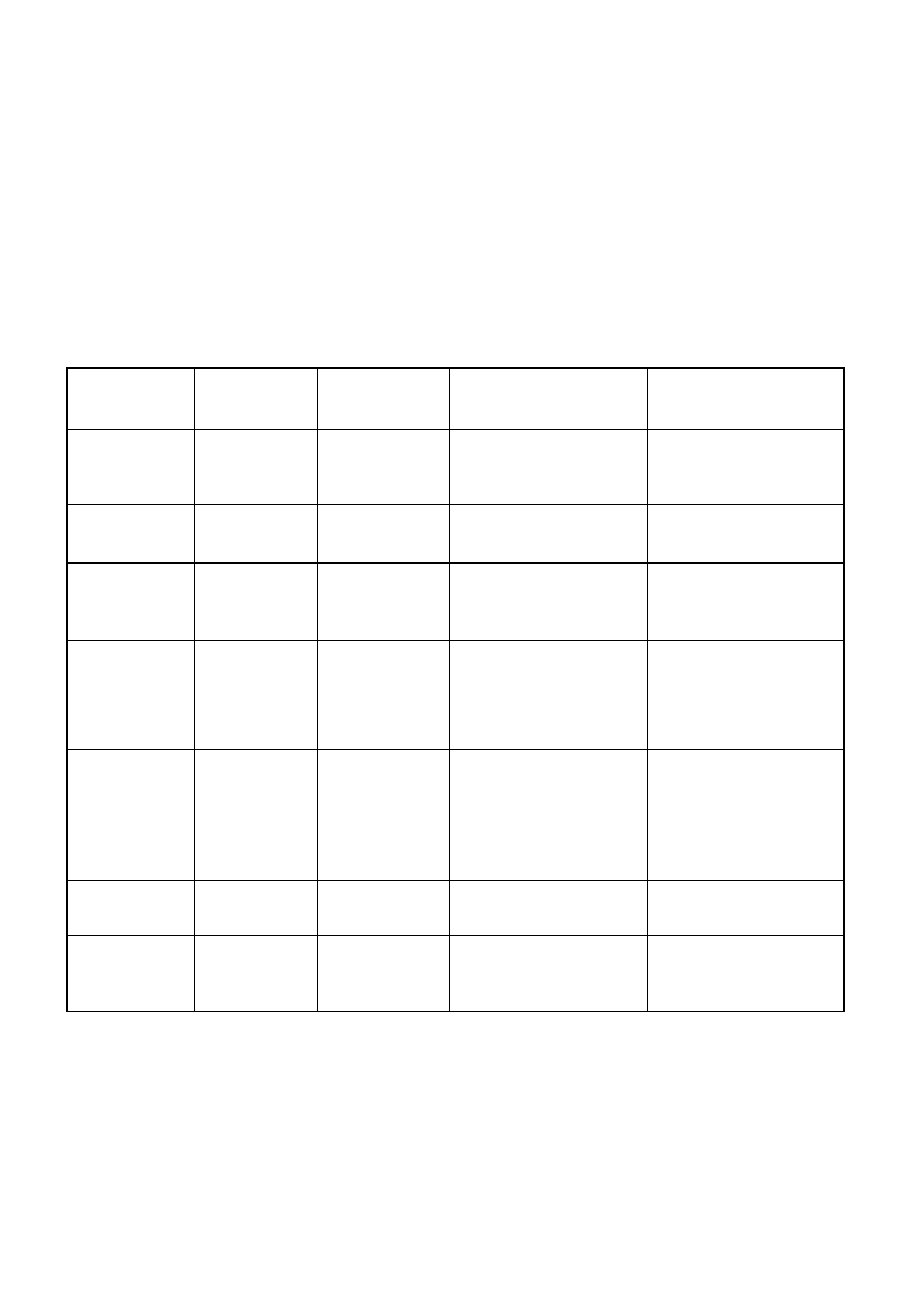
Result for all of the following diagnostic items are displayed on screen. No error has occured if the screen displays a "0".
Diagnostic
Item
Description
· Power does not
turn on
· +B overcurrent
(OCP)
· +B overvoltage
(OVP)
· Vertical deflection
failure
· White balance
failure (no
PICTURE)
· Horizontal
deflection failure
· Micro reset
No. of times
STANDBY/TIMER
lamp flashes
Does not light
2 times
3 times
4 times
5 times
6 times
--
Self-diagnostic
display/Diagnostic
result
--
002:000 or
002:001~255
003:000 or
003:001~255
004:000 or
004:001~255
005:000 or
005:001~255
006:000 or
006:001~225
101:00 or
101:001~225
Probable
Cause
Location
· Power cord is not plugged
in.
· Fuse is burned out F1601
(F1 Board)
· H.OUT Q6807 is shorted.
· H.IN Q6810 is shorted.
Q6802 shorted.
· PH6602 faulty.
D6644 faulty, R6651 open.
· 10.5V is not supplied.
(D board)
· V.OUT IC6800 faulty
D6816 faulty
D6817 faulty
D6824 faulty
R6852 open
R6851 open (D board)
· G2 is improperly adjusted.
(Note 2)
· CRT problem.
· Video OUT IC9001, 9002,
9003 are faulty. (C board)
· IC8306 (A board) and
IC4301 (A board) are faulty.
· C6831 is open circuit.
PS6606 open, PS6605
open. (D board)
· CRT Discharge (C Board)
· Static discharge
· External noise
Detected
Symptoms
· Power does not come on.
· No power is supplied to the
TV.
· AC power supply is faulty.
· Power does not come on.
· Load on power line is
shorted.
· Power does not come on.
· Vertical deflection pulse is
stopped.
· Vertical size is too small.
· Vertical deflection stopped.
· No raster is generated.
· CRT cathode current
detection reference pulse
output is small.
· H pulse output is too high.
· Power is shut down shortly,
after this return back to
normal.
· Detect Micro latch up.
Note 1: Refer to screen (G2) Adjustment in section 5-5 of this manual.
SELF DIAGNOSTIC FUNCTION
5
KV-DR34M69/DR34M89
RM-991
2. DISPLAY OF STANDBY/TIMER LIGHT FLASH COUNT
3. STOPPING THE STANDBY/TIMER FLASH
Turn off the power switch on the TV main unit or unplug the power cord from the outlet to stop the STANDBY/TIMER lamp
from flashing.
4. SELF-DIAGNOSTIC SCREEN DISPLAY
For errors with symptoms such as "power sometimes shuts off" or "screen sometimes goes off" that cannot be confirmed, it
is possible to bring up past occurances of failure for confirmation on the screen:
[To Bring Up Screen Test]
In standby mode, press buttons on the remote commander sequentially in rapid succession as shown below:
[Screen display] / channel [5] / Sound volume [-] / Power ON
Note that this differs from entering the service mode (mode volume [+]).
Self-Diagnosis screen display
Lamp ON 0.3 sec.
Lamp OFF 3 sec.
Lamp OFF 0.3 sec.
2 times
3 times
4 times
5 times
6 times
Diagnostic Item
Flash Count*
+B overcurrent
2 times
+B overvoltage
3 times
V deflection stop
4 times
White balance failure
5 times
Horizontal Deflection Failure
6 times
* One flash count is not used for self-diagnostic.
002 : 000
003 : 000
004 : 000
005 : 001
Numeral "0" means that no fault has been detected.
Numeral "1" means a fault has been detected.
006 : 002
101 : 000
SELF DIAGNOSTIC
Numeral "2" means two faults have been detected.
STANDBY/SLEEP lamp