
TRINITRON
® COLOR TELEVISION
SERVICE MANUAL
DA-4 CHASSIS
MODEL NAME
REMOTE COMMANDER
DESTINATION
CHASSIS NO.
9-965-950-02
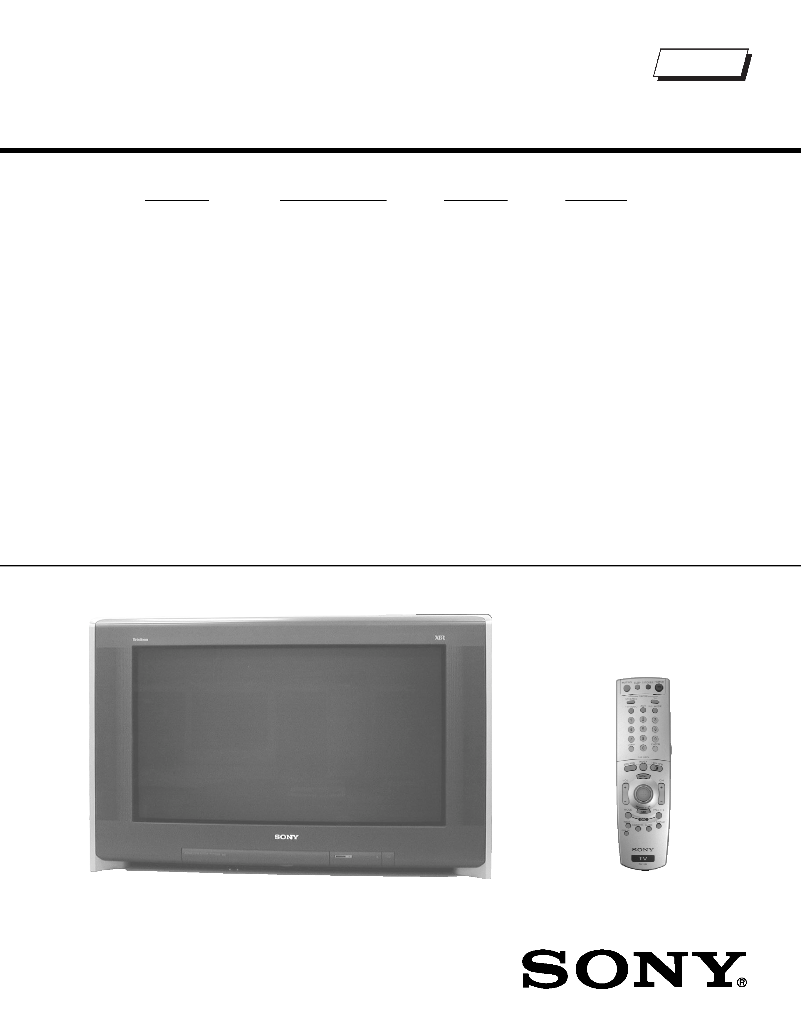
KV-30XBR910
RM-Y188
US
SCC-S66L-A
KV-30XBR910
RM-Y188
CANADA
SCC-S70K-A
KV-30XBR910
RM-Y188
HAWAII
SCC-S69F-A
KV-34XBR910
RM-Y188
US
SCC-S66M-A
KV-34XBR910
RM-Y188
CANADA
SCC-S70L-A
KV-34XBR910
RM-Y188
HAWAII
SCC-S69G-A
HISTORY INFORMATION FOR THE FOLLOWING MANUAL:
ORIGINAL MANUAL ISSUE DATE: 8/2003
REVISION DATE
REVISION TYPE
SUBJECT
8/2003
No revisions or updates are applicable at this time.
1/2004
Added complete Service Data List, Replaced pages 27-29 with pages 27-A through 27-W and 29
(Note: Removed page 28)
Added complete ID Map Table Replaced page 29 with page 29.
TRINITRON
® COLOR TELEVISION
SERVICE MANUAL
DA-4 CHASSIS
MODEL NAME
REMOTE COMMANDER
DESTINATION
CHASSIS NO.
9-965-950-02
KV-30XBR910
RM-Y188
US
SCC-S66L-A
KV-30XBR910
RM-Y188
CANADA
SCC-S70K-A
KV-30XBR910
RM-Y188
HAWAII
SCC-S69F-A
KV-34XBR910
RM-Y188
US
SCC-S66M-A
KV-34XBR910
RM-Y188
CANADA
SCC-S70L-A
KV-34XBR910
RM-Y188
HAWAII
SCC-S69G-A
Self Diagnosis
Supported model
KV-34XBR910
RM-Y188

-- 3 --
KV-30XBR910/34XBR910
TABLE OF CONTENTS
SECTION TITLE
PAGE
SECTION TITLE
PAGE
Specifications ................................................................................. 4
Warnings and Cautions .................................................................. 5
Safety Check-Out ........................................................................... 6
Self-Diagnostic Function................................................................. 7
SECTION 1: DISASSEMBLY............................................................... 10
1-1. Rear Cover Removal............................................................ 10
1-2. Chassis Assembly Removal................................................. 10
1-3. Service Position ................................................................... 10
1-4. Picture Tube Removal...........................................................11
Anode Cap Removal Procedure............................................11
SECTION 2: SET-UP ADJUSTMENTS................................................ 12
2-1. Beam Landing ...................................................................... 12
2-2. V-PIN and V-CEN Adjustment .............................................. 13
2-3. Convergence........................................................................ 13
2-3.1. Vertical and Horizontal Static Convergence ............ 13
2-3.2. Operation of BMC (Hexapole) Magnet .................... 14
2-3.3. TLH Plate Adjustment .............................................. 14
2-3.4. Dynamic Convergence Adjustments........................ 14
2-3.5. Screen-Corner Convergence................................... 15
2-4. Focus Adjustment................................................................. 16
2-4.1. Dynamic Focus/Dynamic Quadra-Pole Data ........... 17
2-5. Screen (G2).......................................................................... 17
2-6. Picture Quality Adjustments ................................................. 17
2-6.1. Video Input - Sub Contrast Adjustment.................... 17
2-6.2. Video Input - Sub Hue/Sub Color Adjustment.......... 17
2-6.3. RF Input - Two Picture Sub Contrast Adjustment .... 18
2-6.4. RF Input - Sub Hue/Sub Color Adjustment .............. 18
2-7. White Balance (CRT) and Sub Bright Adjustment................ 19
2-7.1. Color Offset Adjustment Procedure ......................... 19
2-8. H Raster Center Adjustment ................................................ 19
2-9. Picture Distortion Adjustments ............................................. 20
2-9.1. NTSC (DRC) Full Mode Adjustment ........................ 20
2-9.2. 1080i HD Mode Adjustment ..................................... 21
2-9.3. Twin Mode/Favorite/Index/Normal Mode
Geometry Confirmation............................................ 21
SECTION 3: SAFETY RELATED ADJUSTMENTS............................. 22
3-1. Preparation Before Confirmation.......................................... 22
3-1.1
Hold-Down Operation Confirmation......................... 22
3-2. B+ Max Confirmation ........................................................... 22
3-3. HV Service Flow Chart......................................................... 23
SECTION 4: CIRCUIT ADJUSTMENTS.............................................. 25
4-1. Setting Service Adjustment Mode ........................................ 25
4-1.1. Service Adjustment Mode In .................................... 25
4-1.2. Service Adjustment Mode Memory .......................... 25
4-1.3. Reading the Memory ............................................... 25
4-1.4. Adjusting the Picture................................................ 25
4-1.5. Resetting the Data ................................................... 25
4-1.6. Resetting the MID NVM Data .................................. 25
4-1.7. Resetting the System NVM Data ............................. 25
4-1.8. Copy Function.......................................................... 25
4-2. Memory Write Confirmation Method .................................... 26
4-3. Remote Adjustment Buttons and Indicators ......................... 26
4-4. Service Data Lists ................................................................ 27
4-5. ID Map Table ........................................................................ 29
SECTION 5: DIAGRAMS..................................................................... 30
5-1. Circuit Boards Location ........................................................ 30
5-2. Printed Wiring Boards and
Schematic Diagrams Information ......................................... 30
5-3. Block Diagrams ..................................................................... 31
5-4. Schematics and Supporting Information .............................. 35
UD Board Schematic Diagram ............................................. 35
B Board Schematic Diagram (1 of 6) ................................... 37
B Board Schematic Diagram (2 of 6) ................................... 38
B Board Schematic Diagram (3 of 6) ................................... 39
B Board Schematic Diagram (4 of 6) ................................... 40
B Board Schematic Diagram (5 of 6) ................................... 41
B Board Schematic Diagram (6 of 6) ................................... 42
MX Board Schematic Diagram (1 of 4) ................................ 45
MX Board Schematic Diagram (2 of 4) ................................ 46
MX Board Schematic Diagram (3 of 4) ................................ 47
MX Board Schematic Diagram (4 of 4) ................................ 48
UX Board Schematic Diagram ............................................. 51
HMX Board Schematic Diagram .......................................... 53
V Board Schematic Diagram (1 of 5) ................................... 55
V Board Schematic Diagram (2 of 5) ................................... 56
V Board Schematic Diagram (3 of 5) ................................... 57
V Board Schematic Diagram (4 of 5) ................................... 58
V Board Schematic Diagram (5 of 5) ................................... 59
D Board Schematic Diagram (1 of 2) ................................... 62
D Board Schematic Diagram (2 of 2) ................................... 63
DL Board Schematic Diagram.............................................. 67
HCX Board Schematic Diagram........................................... 70
A Board Schematic Diagram (1 of 2).................................... 72
A Board Schematic Diagram (2 of 2).................................... 73
CX Board Schematic Diagram ............................................. 76
HAX Board Schematic Diagram........................................... 78
HB Board Schematic Diagram ............................................. 79
WX Board Schematic Diagram ............................................ 81
5-5. Semiconductors (1 of 2) ....................................................... 85
Semiconductors (2 of 2) ....................................................... 86
SECTION 6: EXPLODED VIEWS ........................................................ 87
6-1. Chassis ................................................................................ 87
6-2. Picture Tube ......................................................................... 88
6-3. Beznet .................................................................................. 89
SECTION 7: ELECTRICAL PARTS LIST........................................... 90
-- 4 --
KV-30XBR910/34XBR910
SPECIFICATIONS
Design and specifications are subject to change without notice.
SRS (SOUND RETRIEVAL SYSTEM)
The
SRS (SOUND RETRIEVAL SYSTEM) is manufactured
by Sony Corporation under license from SRS Labs, Inc. It is
covered by U.S. Patent No. 4,748,669. Other U.S. and foreign
patents pending.
The word `SRS' and the SRS symbol
are registered trade-
marks of SRS Labs, Inc. BBE and BBE symbol are trademarks of
BBE Sound, Inc. and are licensed by BBE Sound, Inc. under U.S.
Patent No. 4,638,258 and 4,482,866.
TruSurroundTM
by
SRS
®
TruSurround is a trademark of SRS Labs, Inc. SRS and the SRS
symbol are registered trademarks of SRS Labs, Inc. in the United
States and in select foreign countries. SRS and TruSurround are
incorporated under license from SRS Labs, Inc. and are protected
under United States Patent Nos. 4,748,669 and 4,841,572 with
numerous additional issued and pending foreign patents. Pur-
chase of this product does not convey the right to sell recordings
made with the TruSurround technology.
1)
1 Vp-p 75 ohms unbalanced, sync negative
2)
Y: 1 Vp-p 75 ohms unbalanced, sync negative
C: 0.286 Vp-p (Burst signal), 75 ohms
3)
Y: 1.0 Vp-p, 75 ohms unbalanced, sync negative;
P
B
: 0.7 Vp-p, 75 ohms
P
R
: 0.7 Vp-p, 75 ohms
4)
500 mVrms (100% modulation), Impedance: 47 kilohms
5)
More than 408 mVrms at the maximum volume setting (variable)
More than 408 mVrms (fix); Impedance (output): 2 kilohms
6)
3.3V T.M.D.S., 50 ohms
The DVI-HDTV input terminal is complieant with the EIA-861
standard and is not intended for use with personal computers.
KV-30XBR910
KV-34XBR910
Power Requirements
Number of Inputs/Outputs
Video
1)
S Video
2)
Y,PB, PR
3)
Audio
4)
Audio Out
5)
Control-S (In/Out)
DVI-HDTV
6)
Speaker Output (W)
Power Consumption (W)
In Use (Max)
In Standby
Dimensions (W x H x D)
mm
898 x 607 x 563 mm
994 x 652 x 605 mm
in 35
3/8 x 23 7/8 x 22 1/8 in 39 1/8 x 25 5/8 x 23 7/8 in
Mass
kg
70 kg
90 kg
lbs
155 lbs
199 lbs
280W
1W
120V, 60Hz
4
3
2
7
1
YES
1
7.5W x 2
15W Subwoofer
Television system
American TV standard, NTSC
Channel coverage
VHF: 2-13/ UHF: 14-69/ CATV: 1-125
Picture tube
FD Trinitron
®
tube
Visible screen size
30-inch picture measured diagonally (KV-30XBR910
Only)
34-inch picture measured diagonally (KV-34XBR910
Only)
Actual screen size
32-inch measured diagonally (KV-30XBR910 Only)
36-inch measured diagonally (KV-34XBR910 Only)
Antenna
75 ohm external terminal for VHF/UHF
Supplied Accessories
Remote Commander RM-RM-Y188
Two Size AA (R6) Batteries
Optional Accessories
AV Cable: VMC-810/820/830 HG
Audio Cable: RKC-515HG
Component Video Cable: VMC-10/30 HG
TV Stand: SU-30XBR1 (KV-30XBR910 Only)
TV Stand: SU-34XBR1 (KV-34XBR910 Only)

-- 5 --
KV-30XBR910/34XBR910
WARNINGS AND CAUTIONS
CAUTION
Short circuit the anode of the picture tube and the anode cap to the metal chassis, CRT shield, or carbon painted on the CRT, after
removing the anode.
WARNING!!
An isolation transformer should be used during any service to avoid possible shock hazard, because of live chassis. The chassis of
this receiver is directly connected to the ac power line.
! SAFETY-RELATED COMPONENT WARNING!!
Components identified by shading and ! mark on the schematic diagrams, exploded views, and in the parts list are critical for safe
operation. Replace these components with Sony parts whose part numbers appear as shown in this manual or in supplements
published by Sony. Circuit adjustments that are critical for safe operation are identified in this manual. Follow these procedures
whenever critical components are replaced or improper operation is suspected.
ATTENTION!!
Apres avoir deconnecte le cap de l'anode, court-circuiter l'anode du tube cathodique et celui de l'anode du cap au chassis metallique
de l'appareil, ou la couche de carbone peinte sur le tube cathodique ou au blindage du tube cathodique.
Afin d'eviter tout risque d'electrocution provenant d'un chássis sous tension, un transformateur d'isolement doit etre utilisé lors de tout
dépannage. Le chássis de ce récepteur est directement raccordé à l'alimentation du secteur.
! ATTENTION AUX COMPOSANTS RELATIFS A LA SECURITE!!
Les composants identifies par une trame et par une marque ! sur les schemas de principe, les vues explosees et les listes de pieces
sont d'une importance critique pour la securite du fonctionnement. Ne les remplacer que par des composants Sony dont le numero
de piece est indique dans le present manuel ou dans des supplements publies par Sony. Les reglages de circuit dont l'importance
est critique pour la securite du fonctionnement sont identifies dans le present manuel. Suivre ces procedures lors de chaque
remplacement de composants critiques, ou lorsqu'un mauvais fonctionnement suspecte.