TRINITRON® COLOR TELEVISION
SERVICE MANUAL
BA-4DCHASSIS
MODEL NAME
REMOTE COMMANDER
DESTINATION
CHASSIS NO.
9-965-857-02
KV-27S42
RM-Y165
US
SCC-S27H-A
KV-27S42
RM-Y165
CND
SCC-S28F-A
KV-27S46
RM-Y167
US
SCC-S27K-A
KV-27S66
RM-Y167
US
SCC-S27L-A
KV-27S66
RM-Y167
CND
SCC-S28G-A
KV-29AL42
RM-Y165
E
SCC-S25U-A
KV-29AL42C
RM-Y165
E
SCC-S25Y-A
KV-29AL66
RM-Y167
E
SCC-S25T-A
KV-29AL66C
RM-Y167
E
SCC-S25V-A
KV-29SL42
RM-Y165
E
SCC-S25W-A
KV-29SL42C
RM-Y165
E
SCC-S25S-A
KV-29SL46
RM-Y167
E
SCC-S25X-A
KV-29XL42M
RM-Y165
MX
SCC-S26C-A
KV-29SL43
RM-Y165
E
SCC-S55C-A
KV-29SL43C
RM-Y165
E
SCC-S55D-A
HISTORY INFORMATION FOR THE FOLLOWING MANUAL:
ORIGINAL MANUAL ISSUE DATE: 4/1999
REVISION DATE
REVISION TYPE
SUBJECT
4/1999
No revisions or updates are applicable at this time.
6/1999
CORRECTION-1 Updated CRT Part Number for KV-27S66
9/1999
CORRECTION-2 Updated DY Part Number
5/2001
SUPPLEMENT-1 New Model Added: KV-29SL43
8/2001
SUPPLEMENT-2 New Model Added: KV-29SL43C
8/2001
CORRECTION-3 Updated Part Number for Q550 (Pg. 55)
9/2003
CORRECTION-4 Added Connection Point to A Board Schematic (Replaced Pg. 31, 32, 33, & 34)
Updated History Information page (Replaced Pg. 1)
Updated last page to reflect new service manual part number (Replaced last page)
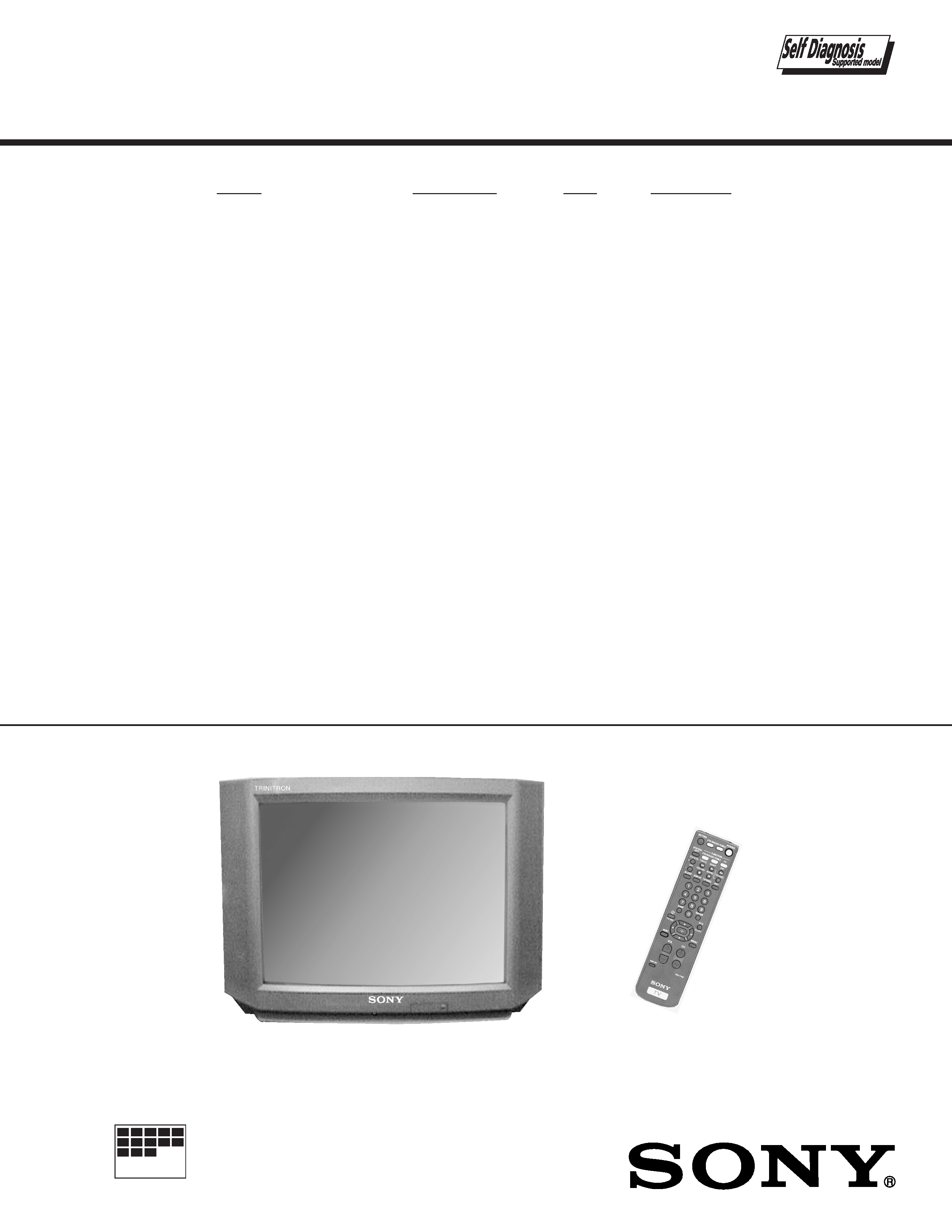
SERVICE MANUAL
BA-4D CHASSIS
MODEL
COMMANDER
DEST
CHASSIS NO.
KV-27S42
RM-Y165
US
SCC-S27H-A
KV-27S42
RM-Y165
CND
SCC-S28F-A
KV-27S46
RM-Y167
US
SCC-S27K-A
KV-27S66
RM-Y167
US
SCC-S27L-A
KV-27S66
RM-Y167
CND
SCC-S28G-A
KV-29AL42
RM-Y165
E
SCC-S25U-A
KV-29AL42C
RM-Y165
E
SCC-S25Y-A
KV-29AL66
RM-Y167
E
SCC-S25T-A
KV-29AL66C
RM-Y167
E
SCC-S25V-A
KV-29SL42
RM-Y165
E
SCC-S25W-A
KV-29SL42C
RM-Y165
E
SCC-S25S-A
KV-29SL46
RM-Y167
E
SCC-S25X-A
KV-29XL42M
RM-Y165
MX
SCC-S26C-A
TRINITRON® COLOR TV
RM-Y167
KV-29AL66
MICROFILM
-- 2 --
KV-27S42/27S46/27S66/29AL42/29AL42C/29AL66/
29AL66C/29SL42/29SL42C/29SL46/29XL42M
KV-29SL46
KV-27S46
KV-29AL42
KV-29AL66C
KV-29XL42M
KV-27S42
KV-27S66
KV-29AL42C
KV-29AL66
KV-29SL42
KV-29SL42C
120-220V
120-220V
120-220V
Power Requirements
120V,60Hz
120V,60Hz
50/60Hz
50/60Hz
50/60Hz
Number of input/outputs
Video1)
12
23
1, 2(KV-29SL46)
S Video2)
11
11
1
Audio3)
12
23
1, 2(KV-29SL46)
Audio Out4)
11
11
1
Monitor Out
--
-
1
-
Speaker Output(W)
5WX2
5WX2
10WX2
10WX2
5WX2
Power Consumption(W)
150W (KV-27S66)
In Use (Max)
140W
140W (KV-27S46)
170W
180W
140W
In Standby
2W
2W
3W
3W
3W
Dimensions(W/H/D)
(mm)
660.4X598
660.4X598
767.4X579.7
767.4X579.7
660.4X598
X505.5mm
X505.5mm
X547.7mm
X547.7mm
X505.5mm
(in.)
26x239/16x20in
26x239/16x20in
301/4X227/8x215/8in
301/4X227/8x215/8in
26x239/16x20in
Mass
(Kg)
39kg
39kg
42kg
42kg
39kg
(lbs)
86lbs
86lbs
93lbs
93lbs
86lbs
SPECIFICATIONS
Television system
American TV standard/NTSC
Channel coverage
VHF:2-13 / UHF:14-69 / CATV:1-125
Picture tube
Trinitron® tube
Visible screen size
27-inch picture measured diagonally
29-inch picture measured diagonally
Antenna
75 ohm external antenna terminal for VHF/UHF
Supplied accessories
Remote Commander with 2 size AA (R6) batteries
RM-Y167 (KV-29AL66/29AL66C/29SL46/27S46/27S66)
RM-Y165 (KV-29AL42/29AL42C/27S42/29XL42M/29SL42/29SL42C)
Optional accessories
Connecting
Cables:
VMC-810S/820S, VMC-720M.
YC-15V/20V, RK-74A
TV Stand:
SU-27A4
U/V Mixer:
EAC-66
Design and specifications are subject to change without notice.
1) 1 Vp-p 75 ohms unbalanced, sync negative
2) Y: 1 Vp-p 75 ohms unbalanced, sync negative
C: 0.286 Vp-p (Burst signal), 75 ohms
3) 500 mVrms (100% modulation), Impedance: 47 kilohms
4) More than 408 mVrms at the maximum volume setting (variable)
More than 408 mVrms (fix); Impedance: 5 kilohms
(
) SRS (SOUND RETRIEVAL SYSTEM)
The (
) SRS (SOUND RETRIEVAL SYSTEM) is manufac-
tured by Sony Corporation under license from SRS Labs,
Inc. It is covered by U.S. Patent No. 4,748,669. Other U.S.
and foreign patents pending.
The word `SRS' and the SRS symbol (
) are registered
trademarks of SRS Labs, Inc.
BBE and BBE symbol are trademarks of BBE Sound, Inc.
and are licensed by BBE Sound, Inc. under U.S. Patent
No. 4,638,258 and 4,482,866.
-- 3 --
KV-27S42/27S46/27S66/29AL42/29AL42C/29AL66/
29AL66C/29SL42/29SL42C/29SL46/29XL42M
Section
Title
Page
Warnings and Cautions ..................................................................................................................................... 4
Self-Diagnostic Function ................................................................................................................................... 4
Safety Check-Out Instructions ........................................................................................................................... 7
1.
GENERAL ............................................................................................................................................................ 8
2.
DISASSEMBLY
2-1.
Rear Cover Removal (KV-27S46/27S66) .............................................................................................................. 11
2-2.
Rear Cover Removal (KV-29SL42/29C/29SL46/29XL42M) .................................................................................. 11
2-3.
Rear Cover Removal (KV-29AL42/42C/29AL66/66C) .......................................................................................... 11
2-4.
Control Switch Removal (KV-29AL42/42C/29AL66/66C) .................................................................................... 11
2-5.
Chassis Assembly Removal (KV-27S46/27S66/29SL42/29C/29SL46/29XL42M) ............................................. 12
2-6.
Chassis Assembly Removal (KV-29AL42/42C/29Al66/66C) .............................................................................. 12
2-7.
Service Position ..................................................................................................................................... 12
2-8.
Picture Tube Removal ........................................................................................................................... 13
3.
SET-UP ADJUSTMENTS
3-1.
Beam Landing ....................................................................................................................................... 14
3-2.
Convergence .......................................................................................................................................... 15
3-3.
Focus ..................................................................................................................................................... 16
3-4.
Screen (G2) ............................................................................................................................................ 16
3-5.
Method of Setting the Service Adjustment Mode ...................................................................................16
3-6.
White Balance Adjustments .................................................................................................................. 16
4.
SAFETY RELATED ADJUSTMENTS
4-1.
R582 and R584 Confirmation Method (HV Hold-Down Confirmation and Readjustments) .......... 17
4-2.
B+ Voltage Confirmation and Adjustment ............................................................................................. 17
5.
CIRCUIT ADJUSTMENTS
5-1.
Setting the Service Adjustment Mode .................................................................................................... 19
5-2.
Memory Write Confirmation Method ..................................................................................................... 19
5-3.
Adjust Buttons and Indicators ............................................................................................................... 19
5-4.
A Board Adjustments ............................................................................................................................. 21
6.
DIAGRAMS
6-1.
Block Diagram ....................................................................................................................................... 23
6-2.
Circuit Board Location ........................................................................................................................... 26
6-3.
Printed Wiring Boards and Schematic Diagrams ................................................................................. 26
· A Board .............................................................................................................................................. 27
· P Board .............................................................................................................................................. 35
· K Board .............................................................................................................................................. 37
· HT Board ............................................................................................................................................ 37
· C Board .............................................................................................................................................. 39
· CV Board ............................................................................................................................................ 40
· E Board .............................................................................................................................................. 42
· HV Board ............................................................................................................................................ 43
6-4.
Semiconductors .................................................................................................................................... 45
7.
EXPLODED VIEW
7-1.
Chassis (KV-27S66) .............................................................................................................................. 46
7-2.
Chassis (KV-27S42/27S46/27SL42/42C/29SL46/29XL42M) .............................................................. 47
7-3.
Chassis (KV-29AL42/29AL42C) ............................................................................................................ 48
7-4.
Chassis (KV-29AL66/66C) .................................................................................................................... 49
8.
ELECTRICAL PARTS LIST ................................................................................................................................................... 50
TABLE OF CONTENTS
-- 4 --
KV-27S42/27S46/27S66/29AL42/29AL42C/29AL66/
29AL66C/29SL42/29SL42C/29SL46/29XL42M
WARNINGS AND CAUTIONS
CAUTION
SHORT CIRCUIT THE ANODE OF THE PICTURE TUBE AND THE
ANODE CAP TO THE METAL CHASSIS, CRT SHIELD, OR CARBON
PAINTED ON THE CRT, AFTER REMOVING THE ANODE.
WARNING!!
AN ISOLATION TRANSFORMER SHOULD BE USED DURING ANY
SERVICE TO AVOID POSSIBLE SHOCK HAZARD, BECAUSE OF
LIVE CHASSIS. THE CHASSIS OF THIS RECEIVER IS DIRECTLY
CONNECTED TO THE AC POWER LINE.
SAFETY-RELATED COMPONENT WARNING!!
COMPONENTS IDENTIFIED BY SHADING AND MARK
ON THE
SCHEMATIC DIAGRAMS, EXPLODED VIEWS, AND IN THE PARTS
LIST ARE CRITICAL FOR SAFE OPERATION. REPLACE THESE
COMPONENTS WITH SONY PARTS WHOSE PART NUMBERS
APPEAR AS SHOWN IN THIS MANUAL OR IN SUPPLEMENTS
PUBLISHED BY SONY. CIRCUIT ADJUSTMENTS THAT ARE
CRITICAL FOR SAFE OPERATION ARE IDENTIFIED IN THIS MANUAL.
FOLLOW THESE PROCEDURES WHENEVER CRITICAL
COMPONENTS ARE REPLACED OR IMPROPER OPERATION IS
SUSPECTED.
ATTENTION
ATTENTION!!
APRES AVOIR DECONNECTE LE CAP DE L'ANODE, COURT-CIRCUITER
L'ANODE DU TUBE CATHODIQUE ET CELUI DE L'ANODE DU CAP AU CHASSIS
METALLIQUE DE L'APPAREIL, OU AU COUCHE DE CARBONE PEINTE SUR LE
TUBE CATHODIQUE OU AU BLINDAGE DU TUBE CATHODIQUE.
ATTENTION!!
AFIN D'EVITER TOUT RESQUE D'ELECTROCUTION PROVENANT D'UN
CHÁSSIS SOUS TENSION, UN TRANSFORMATEUR D'ISOLEMENT DOIT ETRE
UTILISÉ LORS DE TOUT DÉPANNAGE. LE CHÁSSIS DE CE RÉCEPTEUR EST
DIRECTEMENT RACCORDÉ À L'ALIMENTATION SECTEUR.
ATTENTION AUX COMPOSANTS RELATIFS A LA SECURITE!!
LES COMPOSANTS IDENTIFIES PAR UNE TRAME ET PAR UNE MARQUE
SUR LES SCHEMAS DE PRINCIPE, LES VUES EXPLOSEES ET LES LISTES
DE PIECES SONT D'UNEIMPORTANCE CRITIQUE POUR LA SECURITE DU
FONCTIONNEMENT. NE LES REMPLACER QUE PAR DES COMPOSANTS SONY
DONT LE NUMERO DE PIECE EST INDIQUE DANS LE PRESENT MANUEL OU
DANS DES SUPPLEMENTS PUBLIES PAR SONY. LES REGLAGES DE CIRCUIT
DONT L'IMPORTANCE EST CRITIQUE POUR LA SECURITE DU
FONCTIONNEMENT SONT IDENTIFIES DANS LE PRESENT MANUEL. SUIVRE
CES PROCEDURES LORS DE CHAQUE REMPLACEMENT DE COMPOSANTS
CRITIQUES, OU LORSQU'UN MAUVAIS FONTIONNEMENT SUSPECTE.
SELF-DIAGNOSTIC FUNCTION
The units in this manual contain a self-diagnostic function. If an error occurs, the STANDBY/TIMER LED will automatically begin to flash.
The number of times the LED flashes translates to a probable source of the problem. A definition of the STANDBY/TIMER LED flash
indicators is listed in the instruction manual for the user's knowledge and reference. If an error symptom cannot be reproduced, the Remote
Commander can be used to review the failure occurrence data stored in memory to reveal past problems and how often these problems occur.
Diagnostic Test Indicators
When an error occurs, the STANDBY/TIMER LED will flash a set number of times to indicate the possible cause of the problem. If there is
more than one error, the LED will identify the first of the problem areas.
Results for all of the following diagnostic items are displayed on screen. No error has occurred if the screen displays a "0".
Diagnostic Item
No. of times
Display/
Probable Cause
Detected
Description
STANDBY/TIMER
Diagnostic result
Location
Symptoms
lamp flashes
* Power does not turn on
Does not light
* Power cord is not plugged in.
* Power does not come on.
* Fuse is burned out (F5050) (E Board)
* No power is suppled to the TV.
* AC power supply is faulty.
* +B overcurrent (OCP)
2 times
2:0 or 2:1
* H.OUT (Q502) is shorted. (A board)
* Power does not come on.
* IC1751 is shorted. (C board)
* Load on power line is shorted.
* IC1701 is shorted. (CV board)
* Vertical deflection
4 times
4:0 or 4:1
* +13V is not supplied. (A board)
* Has entered standby state after
stopped*
horizontal raster.
* IC 541 is faulty (A board)
* Vertical deflection pulse is stopped.
* Power line is shorted or power supply
is stopped.
* White balance failure
5 times
5:0 or 5:1
* Video OUT (Q306 to 308) is faulty.(A bd)
* No raster is generated.
(not balanced)
* IC301 is faulty. (A board)
* CRT cathode current detection
* G2 is improperly adjusted**.
reference pulse output is small.
* If a +B overcurrent is detected, stoppage of the vertical deflection is detected simulatneously. The symptom that is diagnosed first by the
microcontroller is displayed on the screen.
** Refer to Screen (G2) Adjustment in Section 3-4 of this manual.