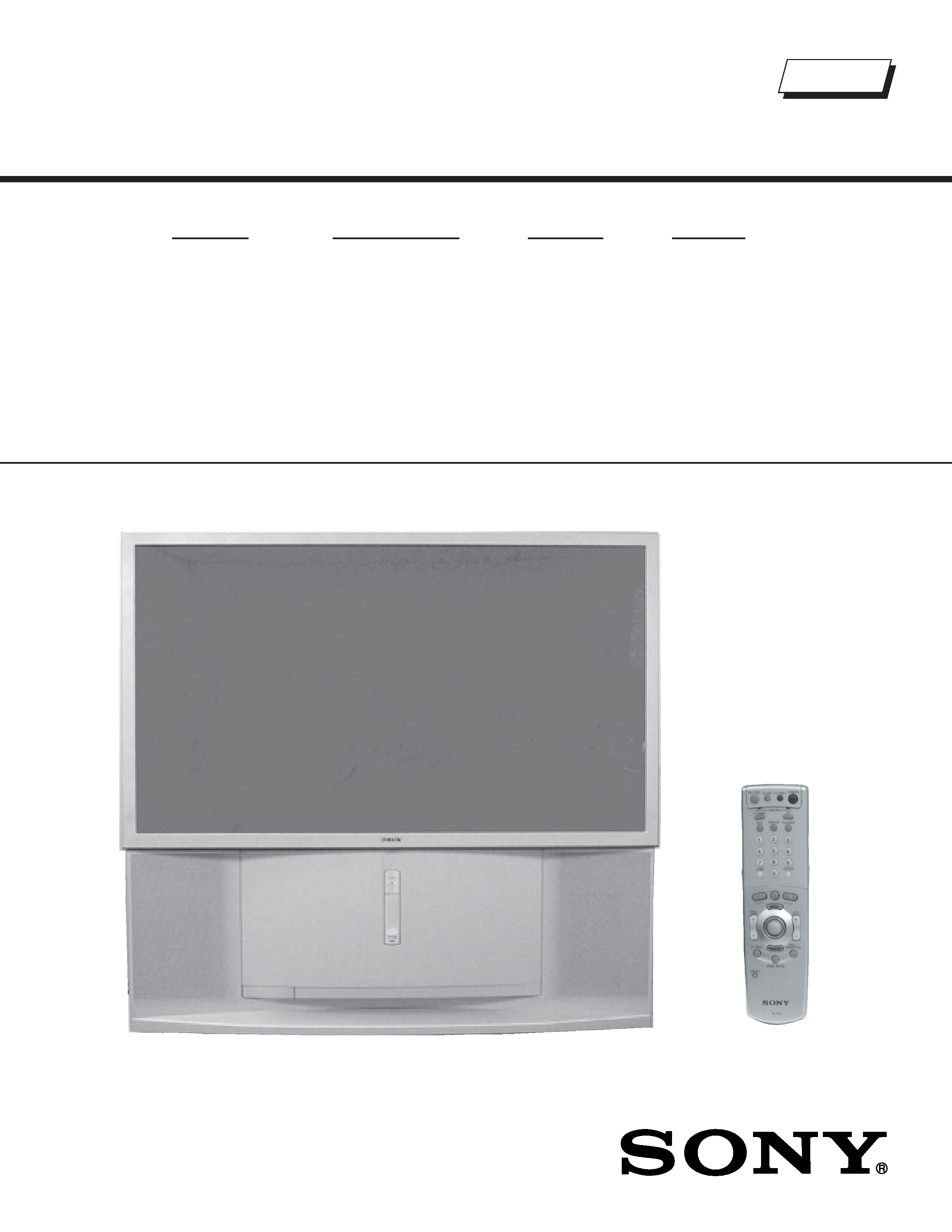
COLOR REAR VIDEO PROJECTION
SERVICE MANUAL
RA-6A CHASSIS
MODEL NAME
REMOTE COMMANDER
DESTINATION
CHASSIS NO.
9-965-944-08
KP-51WS510
RM-Y909
US/CND/LATIN NORTH
SCC-M10CA
KP-57WS510
RM-Y909
US/CND/LATIN NORTH
SCC-M10BA
KP-65WS510
RM-Y909
US/CND/LATIN NORTH
SCC-M10AA
HISTORY INFORMATION FOR THE FOLLOWING MANUAL:
ORIGINAL MANUAL ISSUE DATE: 6/2003
:UPDATED ITEM
REVISION DATE
SUBJECT
6/2003
No revisions or updates are applicable at this time.
6/30/2003
Updated G (Pg. 58) and D (Pg. 77) Schematics,
Added critical symbol to G Board on Exploded View section 6-3. Chassis (Pg. 91)
Updated critical components on Parts Lists (Pgs. 93-136)
8/25/2003
Replaced TV Graphic on Front Cover
Updated Table of Contents (Replace Pg. 3 with Pg. 3)
Corrected Diagrams for H2, H1, and H4 Board Removal (Replace Pg. 11 with Pg. 11)
Replaced 2-11. Service Data Lists with 2-11. Adjustable Service Data Lists
(Replace Pg. 19-37 with Pgs. 19-30)
Corrected procedures for 2-12. Registration Adjustment (Replace Pg. 38 with Pg. 31)
Corrected procedures for 2-13-2. Copying All Registration Data to Other Modes and
2-14. Auto Registration Offsets (Replace Pg. 42 with Pg. 35)
Corrected Error Codes 54 & 55, 2-15. Auto Registration Error Codes (Replace Pg. 43 with Pg. 36)
Added 2-16. Auto Registration Diagnostics (Replace Pg. 44 with Pg. 37)
Corrected 3-D-Comb # from 5-3. Block Diagram (Replace Pg. 51 with Pg. 44)
Deleted IC308 Block Diagram from 5-5. IC Block Diagrams (Replace Pg. 84 with Pg. 77)
Corrected semiconductors 5-6. Semiconductors (Replace Pg. 88 with Pg. 81)
Corrected Grille piece on cover exploded view diagrams (Replace Pgs. 89 & 90 with Pgs. 82 & 83)
9/22/2003
New CRT's & D Board introduced for KP-57WS510/65WS510 models.
Affects S/N's 9,000,001 to 9,700,000
(Replace History Pg., Front Cover, Exploded View Pgs. 84-85, and Parts Lists Pgs. 122, 126, & 129
11/11/2003
Replaced data relating to CR, CG and CB Boards.
Affects Pages 47-49 (Schematics), 85 (Exploded View), 86-88 (Electrical Parts List)
11/16/2004
Removed Note from section 2-12-1. Setup For Adjustment. Note is intended for use by the factory during
production, and should not be performed by service technicians.(Replace Pg. 31 with Pg. 31)
Updated Exploded View section to include new PNs based on serial range
(Replace History Pg., Front Cover, Exploded View Pgs. 82-85, and Parts Lists Pg. 120)
11/17/2003
Corrected serial number range in Electrical Parts List (Replace Parts Lists Pgs. 122 and 126)
8/19/2005
Updated serial number range for D Board and CRTs (Replace Pgs. 84, 85 and 122)
COLOR REAR VIDEO PROJECTION
SERVICE MANUAL
RA-6A CHASSIS
MODEL NAME
REMOTE COMMANDER
DESTINATION
CHASSIS NO.
9-965-944-08
KP-51WS510
RM-Y909
US/CND/LATIN NORTH
SCC-M10CA
KP-57WS510
RM-Y909
US/CND/LATIN NORTH
SCC-M10BA
KP-65WS510
RM-Y909
US/CND/LATIN NORTH
SCC-M10AA
KP-65WS510
RM-Y909
Self Diagnosis
Supported model

-- 3 --
KP-51WS510/57WS510/65WS510
TABLE OF CONTENTS
SECTION TITLE
PAGE
SECTION TITLE
PAGE
Specifications ................................................................................. 4
Warnings and Cautions .................................................................. 5
Safety Check-Out ........................................................................... 6
Self-Diagnostic Function................................................................. 7
SECTION 1: DISASSEMBLY............................................................... 10
1-1. Rear Board Removal............................................................ 10
1-2. Chassis Assembly Removal................................................. 10
1-3. Service Position ................................................................... 10
1-4. H2 Board Removal................................................................11
1-5. H1 Board Removal................................................................11
1-6. H4 Board Removal................................................................11
1-7. Mirror Cover Removal.......................................................... 12
1-8. Beznet Assembly Removal .................................................. 12
1-9. SR Board Removal .............................................................. 12
1-10.AD Board and B Board Removal ......................................... 12
1-11.G Board Removal................................................................. 13
1-12.Terminal Board, A Board, D Board, U Board, and
UD Board Removal .............................................................. 13
1-13.Picture Tube Removal.......................................................... 14
1-14.High-Voltage Cable Installation and Removal...................... 14
SECTION 2: SET-UP ADJUSTMENTS................................................ 15
2-1. Screen Voltage Adjustment (Coarse Adjustment) ................ 15
2-2. Screen (G2) Adjustment (Fine Adjustment).......................... 15
2-3. Deflection Yoke Tilt Adjustment............................................ 15
2-4. Focus Lens Adjustment........................................................ 16
2-5. Focus VR Adjustment........................................................... 16
2-6. 2-Pole Magnet and Centering Magnet Adjustment .............. 17
2-7. Centering Magnet Adjustment.............................................. 17
2-8. 4-Pole Magnet Adjustment................................................... 17
2-9. Blue Defocus Adjustment..................................................... 17
2-10.Electrical Adjustments by Remote Commander................... 18
2-11.Adjustable Service Data Lists .............................................. 19
2-12.Registration Adjustment ....................................................... 31
2-13.PJE Adjustment (Sub Deflection Adjustment) ...................... 33
2-14.Auto Registration Offsets ..................................................... 35
2-15.Auto Registration Error Codes ............................................. 36
2-16.Auto REGISTRATION Diagnostics ...................................... 37
SECTION 3: SAFETY-RELATED ADJUSTMENTS............................. 38
D BOARD ..................................................................................... 38
3-1. HV Regulation Circuit Check and Adjustment ..................... 38
3-2. HV Hold Down Circuit Operation Check and Adjustment .... 38
G BOARD..................................................................................... 39
3-3. +B Max Voltage Confirmation .............................................. 39
3-4. +B OVP Confirmation........................................................... 39
SECTION 4: CIRCUIT ADJUSTMENTS.............................................. 40
4-1. Blue Offset Adjustment......................................................... 40
4-2. P & P Sub Contrast Adjustment (Video) (SCON)................. 40
4-3. P & P Sub Contrast Adjustment (RF) (SCON) ..................... 40
4-4. P & P Sub-Hue and Sub-Color Adjustment (Video)
(SHUE, SCOL)..................................................................... 40
4-5. P & P Sub-Hue and Sub-Color Adjustment (RF)
(SHUE, SCOL)..................................................................... 41
SECTION 5: DIAGRAMS..................................................................... 42
5-1. Circuit Boards Location........................................................ 42
5-2. Printed Wiring Boards and
Schematic Diagrams Information......................................... 42
5-3. Block Diagrams.................................................................... 44
5-4. Schematics and Supporting Information ............................. 47
CR Board Schematic Diagram ............................................ 47
CB Board Schematic Diagram ............................................ 48
CG Board Schematic Diagram ............................................ 49
V Board Schematic Diagram ............................................... 50
G Board Schematic Diagram ............................................... 51
UD Board Schematic Diagram ............................................ 53
A Board Schematic Diagram (1 of 3).................................... 55
A Board Schematic Diagram (2 of 3).................................... 56
A Board Schematic Diagram (3 of 3).................................... 57
U Board Schematic Diagram ............................................... 61
AD Board Schematic Diagram ............................................ 64
B Board Schematic Diagram (1 of 2) ................................... 66
B Board Schematic Diagram (2 of 2) ................................... 67
D Board Schematic Diagram................................................ 70
SR Board Schematic Diagram ............................................ 73
H2 Board Schematic Diagram ............................................. 73
H1 Board Schematic Diagram ............................................. 75
H4 Board Schematic Diagram ............................................. 76
5-5. IC Block Diagrams ............................................................... 77
A Board ................................................................................ 77
B Board ................................................................................ 78
CR Board ............................................................................. 79
CG Board ............................................................................. 79
CB Board.............................................................................. 79
U Board................................................................................ 80
5-6. Semiconductors ................................................................... 81
SECTION 6: EXPLODED VIEWS........................................................ 82
6-1. Cover (KP-51WS510/57WS510 Only) ................................ 82
6-2. Cover (KP-65WS510 0nly)................................................... 83
6-3. Chassis ................................................................................ 84
6-4. Picture Tube......................................................................... 85
SECTION 7: ELECTRICAL PARTS LIST............................................ 86
-- 4 --
KP-51WS510/57WS510/65WS510
120V AC, 60Hz
230W
Under 1 W
DVI-HDTV
1 terminal, 3.3V T.M.D.S., 50 ohms
The DVI-HDTV input terminal is compliant with the EIA-861 stand-
ard and is not intended for use with personal computers.
Video (IN)
4 total (1 on front panel)
1Vp-p, 75ohms unbalanced, sync negative
S Video (IN)
3 total (1 on front panel)
Y: 1Vp-p, 75ohms unbalanced, sync negative
C: 0.286Vp-p (Burst signal), 75ohms
Audio (IN)
6 total (1 on front panel)
500 mVrms (100% modulation)
Impedance:47 kilo ohms
Projection System
3 picture tubes, 3 lenses, horizontal in-line system
Picture Tube
7-inch high-brightness monochrome tubes (6.3 raster size),
with optical coupling and liquid cooling system.
Projection Lenses
High performance, large diameter hybrid lens F1.1
Antenna
75 ohm external terminal for VHF/UHF
Television System
NTSC, American TV Standard
Channel Coverage
VHF: 2-13/ UHF: 14-69/ CATV: 1-125
SPECIFICATIONS
Design and specifications are subject to change without notice.
Power Requirements
Power Consumption (W)
In Use (Max)
In Standby
Inputs/Outputs
Screen Size (measured diagonally)
51 inches (KP-51WS510)
57 inches (KP-57WS510)
65 inches (KP-65WS510)
Supplied Accessories
Remote Control RM-Y909
Batteries (2) size AA (R6)
Optional Accessories
A/V Cable (VMC-810/820/830 HG)
Audio Cable (RKC-515HG)
Component Video Cable (VMC-10/30 HG)
Control S Cable (RK-G69HG)
AV Receiver (STR-V555ES or equivalent)
Audio (VAR/RIX)
1 total
500 mVrms at the maximum volume setting (Variable)
500 mVrms (Fixed)
Impedance (Output):1 kilo ohm
TV Out
1 total
Video: 1 Vp-p 75 ohms unbalanced, Sync negative
Audio: 500 m Vrms (100% modulation)
Impedance (output): 1 kilo ohms
Control S (IN/OUT)
1 total
Minijacks
Component Video Input
2 (Y, PB, PR)
Y: 1.0 Vp-p, 75 ohms unbalanced, sync negative
PB: 0.7 Vp-p, 75 ohms;
PR: 0.7 Vp-p, 75 ohms
RF Inputs
2 total
Converter
1 total
KP-51WS510
KP-57WS510
KP-65WS510
20W x 2
1194 x 1350 x 650 mm
1326 x 1377 x 690 mm
1542 x 1466 x 750 mm
47 x 531/8 x 255/8 in
521/4 x 541/4 x 271/4 in
603/4 x 573/4 x 291/2 in
78.2 kg
88.6 kg
136 kg
172 lbs
195 lbs
300 lbs
Speaker Output (W)
Dimensions (W x H x D)
mm
in
Mass kg
lbs

-- 5 --
KP-51WS510/57WS510/65WS510
WARNINGS AND CAUTIONS
CAUTION
Short circuit the anode of the picture tube and the anode cap to the metal chassis, CRT shield, or carbon painted on the CRT, after
removing the anode.
WARNING!!
An isolation transformer should be used during any service to avoid possible shock hazard, because of live chassis. The chassis of
this receiver is directly connected to the ac power line.
! SAFETY-RELATED COMPONENT WARNING!!
Components identified by shading and ! mark on the schematic diagrams, exploded views, and in the parts list are critical for safe
operation. Replace these components with Sony parts whose part numbers appear as shown in this manual or in supplements
published by Sony. Circuit adjustments that are critical for safe operation are identified in this manual. Follow these procedures
whenever critical components are replaced or improper operation is suspected.
ATTENTION!!
Apres
de l'appareil, ou la couche de carbone peinte sur le tube cathodique ou au blindage du tube cathodique.
Afin d'evite
dépannage. Le chássis de ce récepteur est directement raccordé à l'alimentation du secteur.
! ATTENTION AUX COMPOSANTS RELATIFS A LA SECURITE!!
Les composants identifies par une trame et par une marque ! sur les schemas de principe, les vues explosees et les listes de pieces
sont d'une importance critique pour la securite du fonctionnement. Ne les remplacer que par des composants Sony dont le numero
de piece est indique dans le present manuel ou dans des supplements publies par Sony. Les reglages de circuit dont l'importance
est critique pour la securite du fonctionnement sont identifies dans le present manuel. Suivre ces procedures lors de chaque
remplacement de composants critiques, ou lorsqu'un mauvais fonctionnement suspecte.