SERVICE MANUAL
MODEL
COMMANDER
DEST.
CHASSIS NO.
Please file according to model size. ...
51
CHASSIS
RE-2D
PROJECTION TV
KP-51DS1U
RM-892
UK
SCC-P26B-A
RM-892
2
0
5
8
1
4
7
3
6
9
OK
2
KP-51DS1U
KRM-892
TV system
I
Colour system
PAL
NTSC 3.58, 4.43 (only Video In)
Channel coverage
UHF:
B21-B69
Projected picture size
51 inches
Approx. 130 cm measured diagonally
Rear Terminals
·
Centre speaker input terminals (2
terminals)
·
(L,R) audio outputs (phono jacks)
·
:1/
21-pin Euro connector (CENELEC
standard) including audio/video input,
RGB input, TV audio/video output
·
:2/q 2 21-pin Euro connector (CENELEC
standard) including audio/video input,
S video input, selectable audio/video
output
·
:3
21-pin Euro connector (CENELEC
standard) including audio/video input,
selectable audio/video output (selectable
the same output source as
:2/ s 2
connector)
·
PCMCIA socket
·
MODEM connection
Front Terminals
2 video input - phono jack
2
audio inputs - phono jacks
s
S video input - 4 pin DIN
Headphones jack - minijack stereo
C
Sound output
2 x 30 W (music power)
2 x 15 W (RMS)
Centre SP input
30 W (RMS) (using as the centre speaker)
Power consumption
165 W
Standby Power consumption
0.7 W
Dimensions (w x h x d)
Approx. 1256 x 1264 x 650 mm
Weight
Approx. 63 kg
Accessories supplied
1 Remote Control (RM-892)
2 Batteries (IEC designated)
Other features
Digital Comb filter (High resolution)
TELETEXT, Fastext, EPG
NICAM
Sleep Timer
Smartlink
PCMCIA connection
MODEM connection
Digital terrestrial reception
Design and specifications are subject to change without notice.
2
CAUTION
SHORT CIRCUIT THE ANODE OF HTE PICTURE TUBE
AND THE ANODE CAP TO THE METAL CHASSIS, CRT
SHIELD, OR CARBON PAINTED ON THE CRT, AFTER
REMOVING THE ANODE.
SAFETY-RELATED COMPONENT WARNING!!
COMPONENTS IDENTIFIED BY SHADING AND MARK
0 ON THE SCHEMATIC DIAGRAMS, EXPLODED
VIEWS AND IN THE PARTS LIST ARE CRITICAL TO
SAFE OPERATION. REPLACE THESE COMPONENTS
WITH SONY PARTS WHOSE PART NUMBERS AP-
PEAR AS SHOWN IN THIS MANUAL OR IN SUPPLE-
MENTS PUBLISHED BY SONY.
SPECIFICATIONS

3
KP-51DS1U
KRM-892
1. SELF DIAGNOSIS FUNCTION ......................
4
2. GENERAL .................................................................
10
3. DISASSEMBLY
3-1.
Rear Board Removal .........................................
25
3-2.
Main Bracket Block Removal ...........................
25
3-3.
Service Position .................................................
25
3-4.
Control Panel Block and Resistor
Assembly (Focus Pack) Removal .....................
26
3-5.
Beznet Block Removal ......................................
26
3-6.
Chassis Block Removal ......................................
27
3-7.
Terminal Board Removal ...................................
28
3-8.
A3, U, A and D Boards Removal ......................
28
3-9.
N and A2 Boards Removal ................................
29
3-10. E Board Removal ...............................................
29
3-11. G Board Removal ...............................................
30
3-12. High-Voltage Cable Removal and Installation ..
30
3-13. Picture Tube Removal ........................................
30
4. SET-UP ADJUSTMENTS
4-1.
Screen Voltage Adjustment
(Rough Alignment) ...........................................
31
4-2.
Focus Adjustment ..............................................
31
4-3.
Screen (G2) Adjustment ....................................
31
4-4.
Deflection Yoke Tilt Adjustment ......................
31
4-5.
2-Pole Magnet Adjustment ................................
32
4-6.
4-Pole Magnet Adjustment ................................
32
4-7.
Defocus Adjustment (Blue) ...............................
32
4-8.
Green and Red Focus Adjustment
4-8-1. Green and Red Lens Focus Adjustment .......
32
4-8-2. Green and Red Electrical Focus
Adjustment ....................................................
32
5. SAFETY RELATED ADJUSTMENT
5-1.
HV Hold Down Adjustment .............................
33
6. REGISTRATION ADJUSTMENTS
6-1.
How to Enter the Service Mode
6-1-1. Adjustment Method with Commander ..........
34
6-1-2. Screen Display on the Test Menu ..................
34
6-1-3. Service List (Convergence) ...........................
36
6-2.
PAL Registration Adjustment
6-2-1. Registration Adjustment Method ..................
39
6-2-2. Geometry Adjustment ....................................
39
6-2-3. Convergence Adjustment ...............................
40
TABLE OF CONTENTS
6-3.
Text Position Adjustment ...................................
45
6-4.
White Balance Adjustment ................................
45
6-5.
Sub Bright Adjustment .......................................
45
7. DIAGRAMS
7-1.
Block Diagrams ..................................................
47
7-2.
Frame Schematic Diagram .................................
65
7-3.
Circuit Boards Location .....................................
68
7-4.
Schematic Diagrams and Printed Wiring
Boards .................................................................
68
(1)
Schematic Diagram of A (1/3) Board ................
71
(2)
Schematic Diagram of A (2/3) Board ...............
74
(3)
Schematic Diagram of A (3/3) Board ...............
77
(4)
Schematic Diagram of A3 Board .......................
80
(5)
Schematic Diagram of A2 Board ......................
83
(6)
Schematic Diagram of D Board .........................
86
(7)
Schematic Diagram of E Board .........................
95
(8)
Schematic Diagrams of ZG and ZR Boards ......
98
(9)
Schematic Diagram of N (1/4) Board ................ 101
(10) Schematic Diagram of N (2/4) Board ................ 104
(11) Schematic Diagram of N (3/4) Board ................ 107
(12) Schematic Diagram of N (4/4) Board ................ 110
(13) Schematic Diagrams of CB, CG and
CR Boards .......................................................... 113
(14) Schematic Diagrams of G, H1, H2, H3
and U Boards ...................................................... 116
7-5.
Semiconductors ................................................. 122
8. EXPLODED VIEWS
8-1.
Screen and Cover Block ................................... 125
8-2.
Control Panel and Cabinet Block ...................... 126
8-3.
Main Bracket Block ........................................... 127
8-4.
Picture Tube Block ............................................. 128
9. ELECTRICAL PARTS LIST ............................ 129
Section
Title
Page
Section
Title
Page
4
KP-51DS1U
KRM-892
SECTION 1
SELF DIAGNOSIS FUNCTION
Diagnostic Errors
The errors indicated below can be read using an Error Reader Display (Part Number S-188-900-10) connected to the service connector.
Once an error has been detected it will then be displayed on the two digit error reader.
During the power up procedure and during normal run time, the micro's self diagnostic procedures monitor for various errors, as
described in the table below:
Error Number
Error Description
00
No error (TV Error Reader shows 00 in normal condition)
01
Not allowed (may be confused with Sircs response flash on LED)
02
Protection circuit trip (OCP, OVP & No V-Sync)
03
Reserved for OVP (Included in error 2 for BE-3E)
04
Reserved for No V-Sync (Included in error 2 for BE-3E)
05
AKB
06
IIC Scl Low < Power Up Only >
07
IIC Sda Low < Power Up Only >
08
IIC Sda & Scl Low < Power Up Only >
09
Jungle controller no acknowledge < Power Up Only >
10
Video Switch (CXA2040) no acknowledge < Power Up Only >
11
Tuner no acknowledge
12
MSP no acknowledge
13
NVM no acknowledge
14
AV Switch (CXA2089) no acknowledge (DS10 & DX10)
15
Not Used
16
Port Expander (CXA1875) no acknowledge (DS10 & DX10)
17
Not Used
18
Dynamic Convergence (CXA8070) no acknowledge (Not used for RE-2D)
19
Cannot initialize jungle (after initial power on check OK) - < Chassis Initialization >
20
Jungle controller response failure after power up check (+9V test)
21
Video Switch (CXA2040) cannot power on reset - < Chassis Initialization >
22
Video Switch (CXA2040) response failure after power up check (+9V test)
23
NVM acknowledge fail after initialization (STBY +5V - same as micro!)
24
MSP run-time failure < May Not Be Fatal - Display On Error Reader >
25
DSP run-time failure < May Not Be Fatal - Display On Error Reader >
26
M3L bus Clock low time out after data send < Run-Time Failure >
27
M3L bus Clock low time out after data send < At Power Up Check >
28
M3L bus Clock low time out after data send < At Initialization >
29
M3L Txd Low < Power Up Only >
30
M3L Rxd Low < Power Up Only >
31
M3L Enable Low < Power Up Only >
32
Compact Text test fail < Power Up Only >
33
Compact Text does not respond (+5V test)
34
Compact text run-time failure < May Not Be Fatal - Display On Error Reader >
5
KP-51DS1U
KRM-892
Protection Error (Error 2):
Once every main loop (approximately 200ms OSD mode, 50ms text or menu mode), the micro checks the protection pin (pin 66). If the
protection pin is high 6 successive times, a protection error is diagnosed. The protection pin is not checked during the first 3-4 seconds
after AC on.
If this error is diagnosed, the respective NVM register will be updated and the set goes straight into diagnostic standby with 2 flashes
- no reset is attempted.
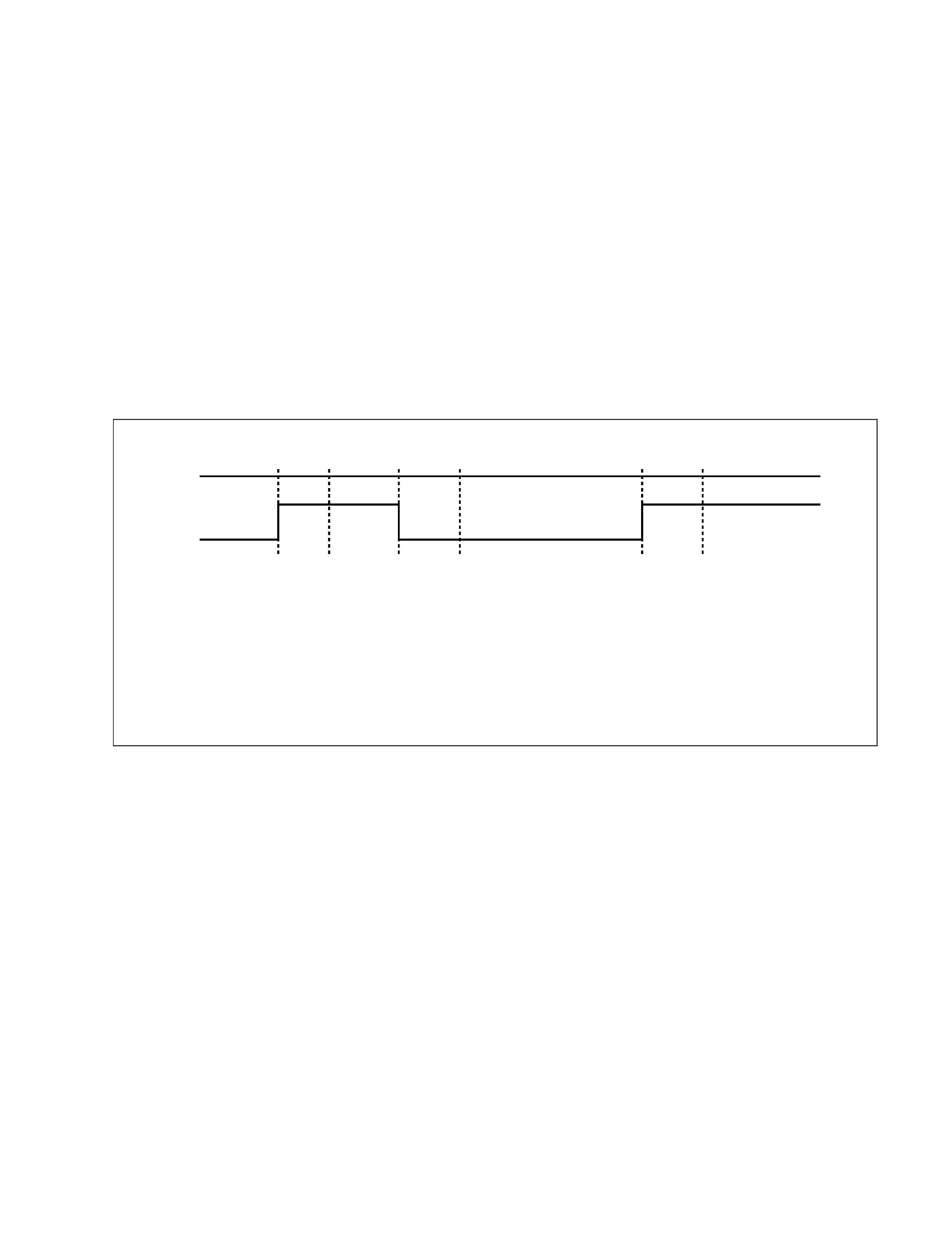
AKB Error (Error 5):
Once every main loop the micro checks the AKB stability by reading the IKR return from the jungle. IKR=1 means that AKB is stable,
IKR=0 means that AKB is unstable. If the AKB status is unstable for 10 seconds, an AKB error is diagnosed. AKB stability is not
checked during the first 20 seconds after AC on.
If this error is diagnosed, the respective NVM register will be updated and the response LED will flash 5 times continually, but the set
will not go into standby. If the AKB status becomes stable, and remains stable for 10 seconds, the LED will stop flashing.
A.
IKR Return first goes high after 12 seconds
B.
Micro begins checking IKR Return status 20 seconds after power on
C.
Micro detects IKR return=0
D.
Micro detects that IKR has been 0 for 10 seconds; NVM counter is incremented and the LED starts flashing (flashes
5 times, off for 2 seconds, flashes 5 times, etc.)
E.
Micro detects that IKR=1; LED continues to flash
F.
Micro detects that IKR has been high for 10 seconds; LED stops flashing.
Startup Diagnostic Errors (Errors 6-18, 27, 29-32):
These errors are checked for during the power up sequence before attempting to retrieve data from the NVM.
6 - SCL pin low
7 - SDA pin low
8 - Both the SCL and the SDA pin are low
9 - No acknowledge from the jungle (CXA2076)
10 - No acknowledge from the video switch (CXA2040)
11 - No acknowledge from the tuner
12 - No acknowledge from the MSP
13 - No acknowledge from the NVM
14 - No acknowledge from the CXA2089 video switch (DS10 & DX10)
16 - No acknowledge from the CXA1875 Port Expander (DS10 & DX10)
18 - No acknowledge from the Dynamic Convergence (CXA8070) : Not used for RE-2D
27 - M3L_TXD pin low after Compact Text RAM test
29 - M3L_TXD pin low
30 - M3L_RXD pin low
31 - M3LEN pin low
32 - Compact Text RAM test fail
If any of these errors are detected, the respective NVM register will be incremented. The software will then carry on with the power up
sequence.
010
AB
C
D
E
F
20
30
40
50
60
70
80
90
100
IKR
Return
Time/seconds