
1
SERVICE MANUAL
Canadian Model
E Model
IT-B7
TELEPHONE
Dial signal
Tone, 10 PPS (pulse) selectable
Dimensions
Approx. 165.5
× 84 × 219 mm (w/h/d)
(Approx. 6 5/8
× 3 3/8 × 8 5/8 inches)
Mass
Approx. 510 g
(Approx. 1 lb. 2 oz.)
Supplied accessories
Telephone line cords (2) (Canadian)
Telephone line cord (1) (E, SP)
Wall bracket (1) (Canadian)
Design and specifications are subject to change without notice.
· Abbreviation
SP : Singapore model
SPECIFICATIONS
Notes on Chip Component Replacement
· Never reuse a disconnected chip component.
· Notice that the minus side of a tantalum capacitor may be
damaged by heat.
MICROFILM
Photo : Gray type
REVISED
2
SECTION 1
GENERAL
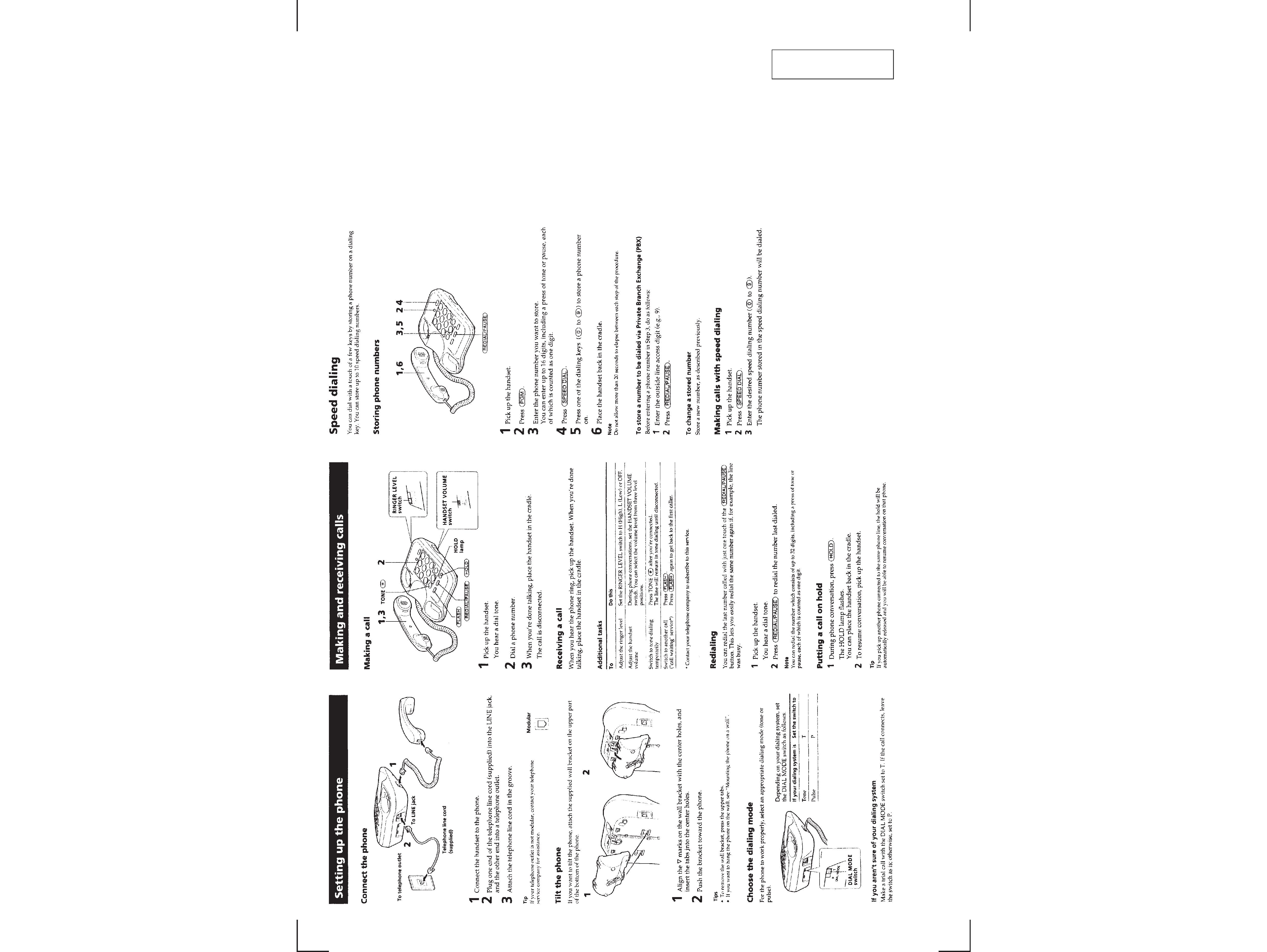
This section is extracted
from instruction manual.
3
4
SECTION 2
DISASSEMBLY
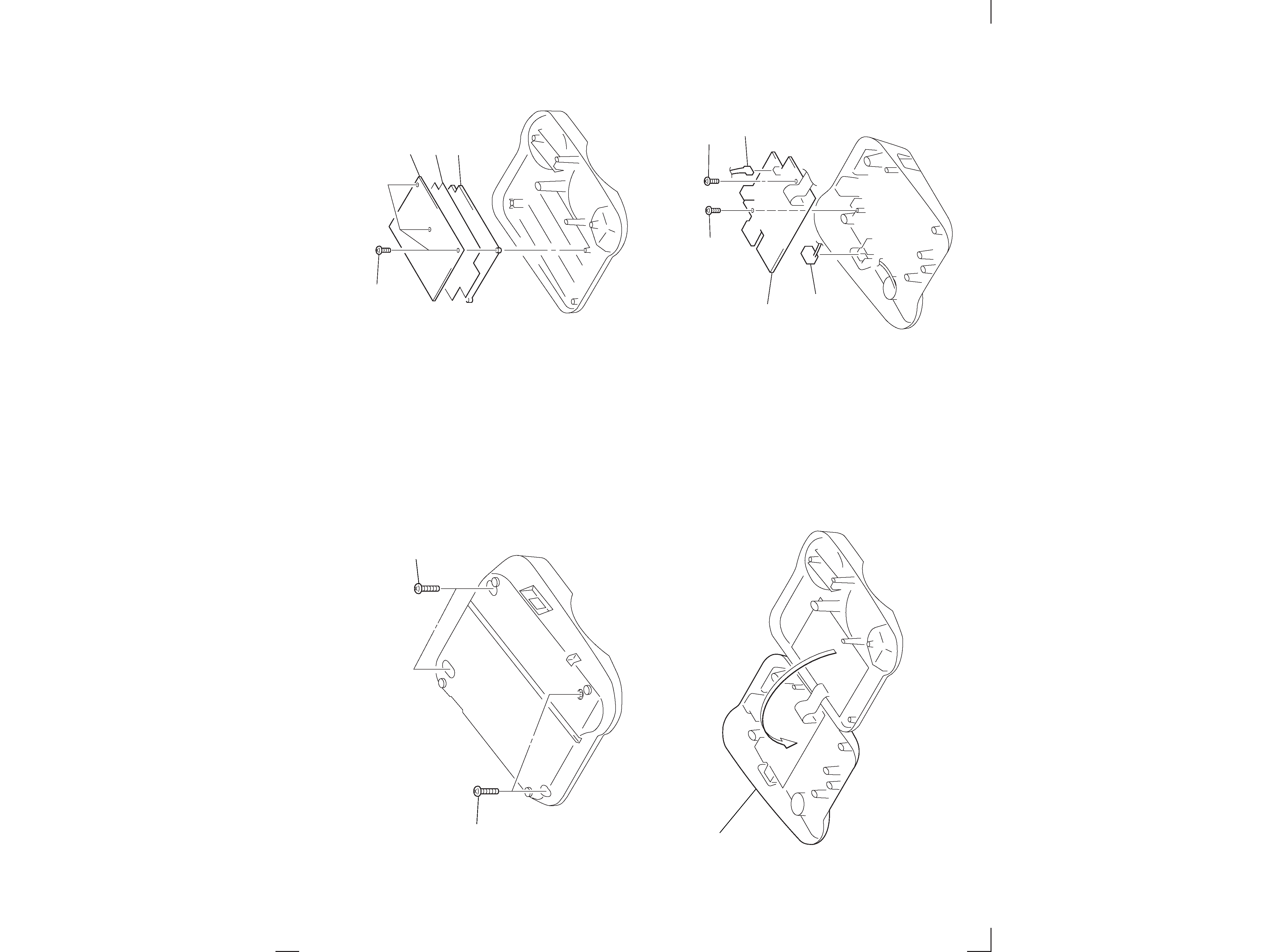
Note : Follow the disassembly procedure in the numerical order given.
2-1. CABINET (LOWER)
3 cabinet (lower)
1 BTP 2.6X6
2 KEY board
3 rubber key switch
4 button (12 key)
1 JP2
2 BTP 2.6X6
3 BTP 2.6X6
4 MAIN board
5 modular jack
1 BTP 3X10
2 BTP 3X10
2-2. KEY BOARD
2-3. MAIN BOARD
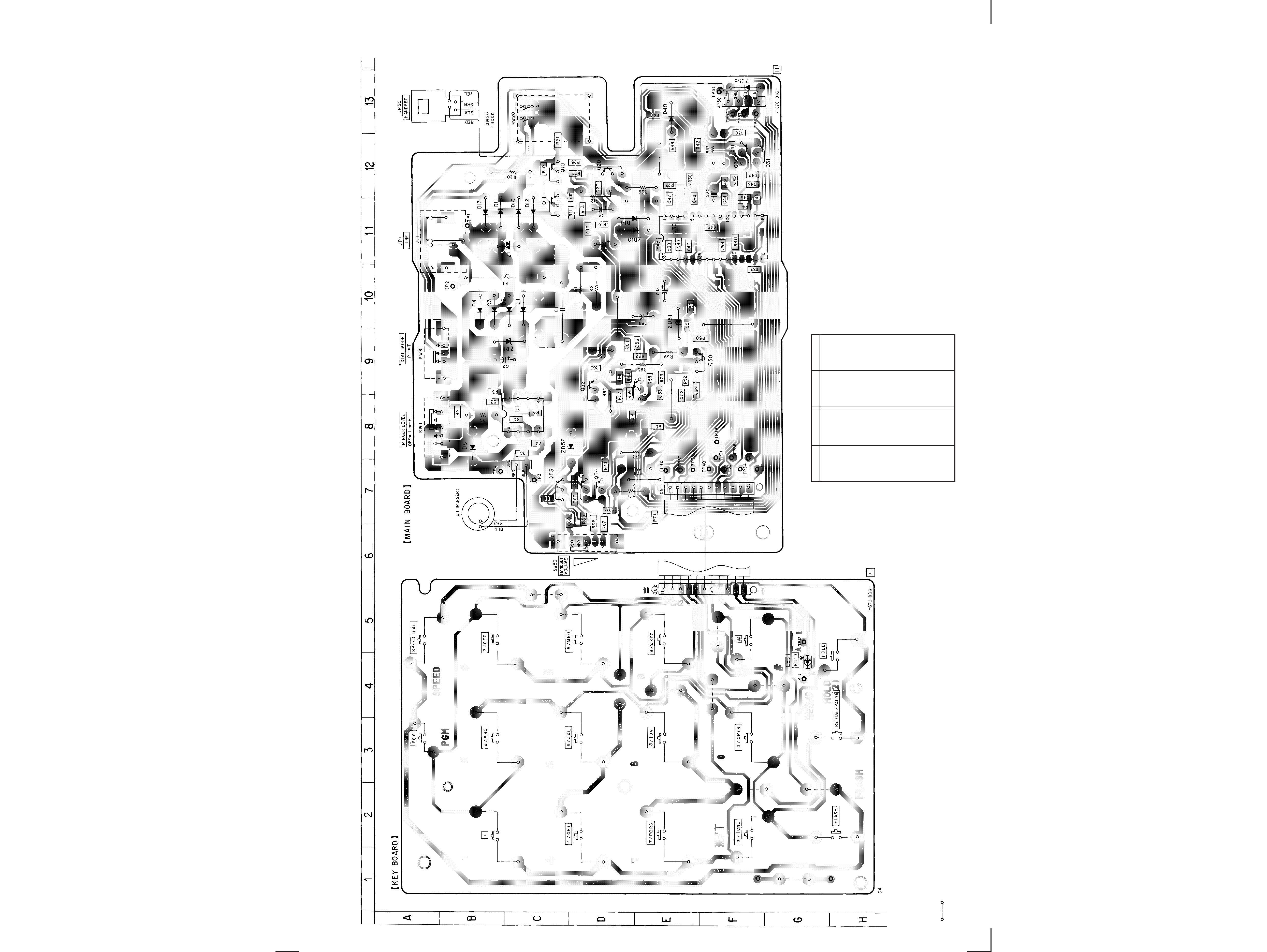
3-1. PRINTED WIRING BOARDS -- Canadian Model --
IT-B7
5
6
SECTION 3
DIAGRAMS
Q30
F-12
Q31
F-12
Q50
E-8
Q51
E-8
Q52
D-9
Q53
C-7
Q54
D-7
Q55
D-7
U1
C-8
U30
D-11
ZD1
C-9
ZD10
D-11
ZD51
D-10
ZD52
C-8
ZD55
F-13
D1
C-10
D2
C-10
D3
B-10
D4
B-10
D5
B-8
D10
D11
B-11
D12
D13
B-11
D14
D-11
D40
E-13
LED1
G-4
Q10
C-12
Q11
C-11
Q20
D-12
Ref. No.
Location
· Semiconductor Location
Ref. No.
Location
Note:
· X : parts extracted from the component side.
·
: Carbon pattern
· b : Pattern from the side which enables seeing.
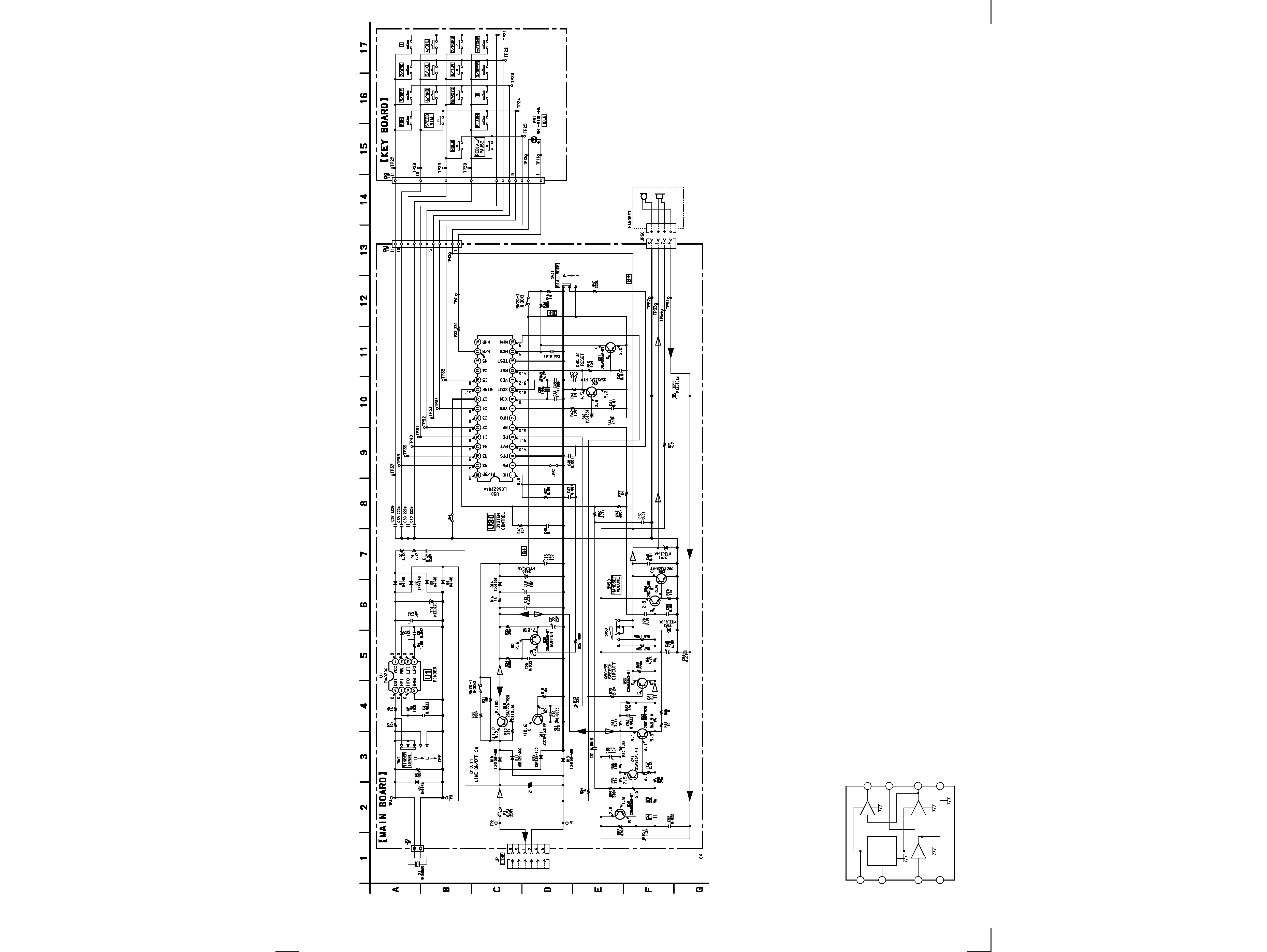
3-2. SCHEMATIC DIAGRAM -- Canadian Model --
IT-B7
7
8
· IC Block Diagram
U1 BA8206
1
2
3
4
5
6
7
8
LOW
FREQ.
OSC
HIGH
FREQ.
OSC
POWER
SUPPLY
WITH
HYSTERESIS
AMP
VCC
RSL
LFI
LFO
OUT
HFI
HFO
GND
Note:
· All capacitors are in
µF unless otherwise noted. pF: µµF
50 WV or less are not indicated except for electrolytics
and tantalums.
· All resistors are in
and 1/4 W or less unless otherwise
specified.
· C : panel designation.
· U : B+ Line.
· Power voltage is dc 12 V and fed with regulated dc power
supply from JP1 with 100
in series.
· Voltage is dc with respect to ground under no-signal
condition.
no mark : OFF HOOK
(
) : ON HOOK
· Voltages are taken with a VOM (Input impedance 10 M
).
Voltage variations may be noted due to normal produc-
tion tolerances.
· Signal path.
N
: RX
O
: TX