MICROFILM
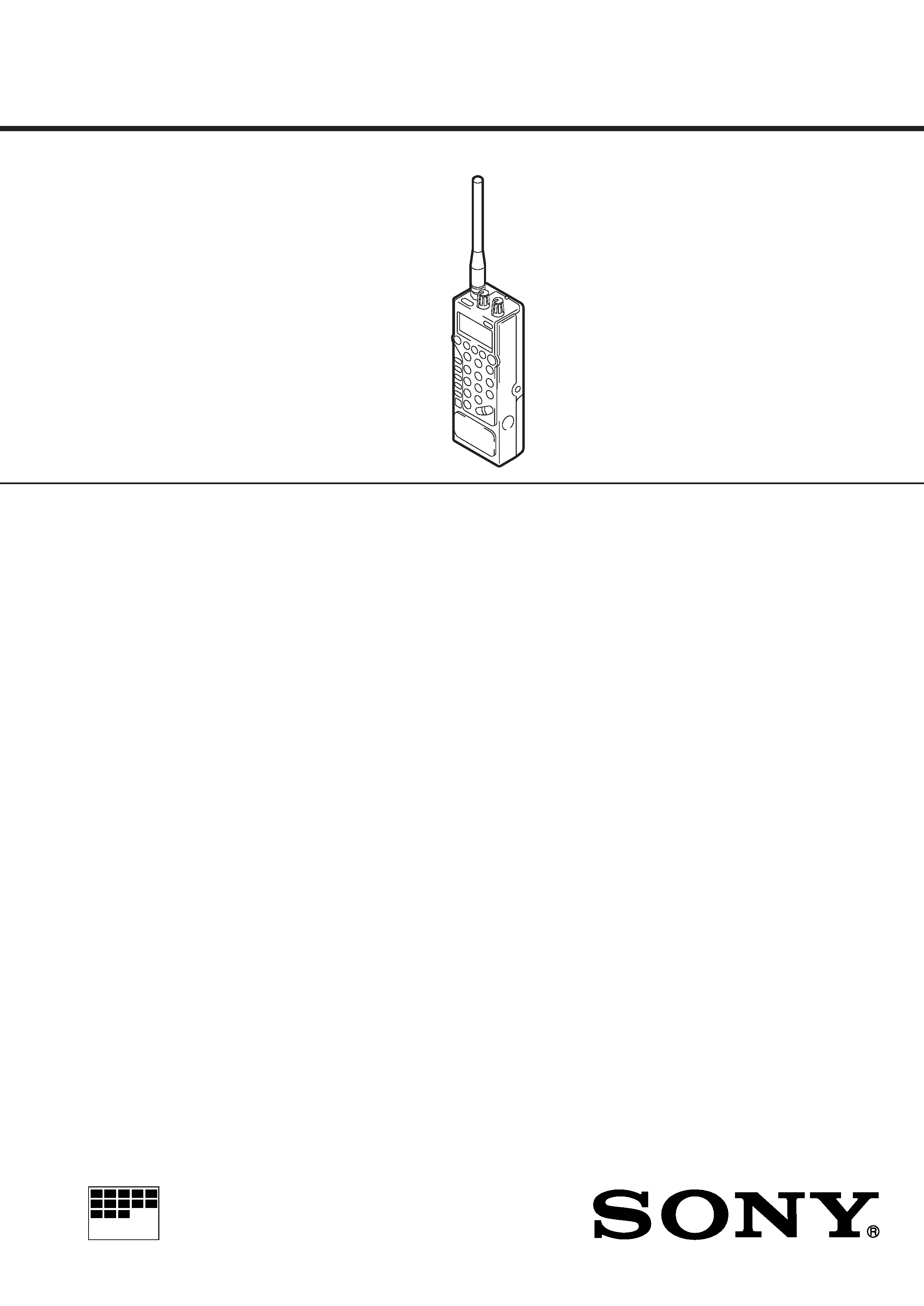
ICF-SC1/SC1PC
SERVICE MANUAL
PLL SYNTHESIZED SCANNING RECEIVER
SPECIFICATIONS
US Model
Circuit system :
Triple conversion superheterodyne
Frequency range :
25.000 1300.000MHz
(excluding cellular phone band : 823.980 849.020 MHz and
868.980 894.020 MHz)
Detection mode :
AM, NFM, WFM
Speaker : Approx. 36 mm (1 7/16 inches) dia., 8 ohms
Power output :
150mW(at 10% harmonic distortion
Output :
@ jack (monaural minijack)
Power requirements :
DC 6V, four size AA (R6) batteries
External power source :
DC 6V
Dimensions :
Approx. 64 x 177 x 44.3 mm (w/h/d) (2 5/8 x 7 x 1 3/4 inches)
incl. projecting parts and controls, not including the helical
antenna and the belt holder
Mass :
Approx. 252g (8.9 oz)
Approx. 382g (13.5 oz) incl. alkaline batteries, helical
antenna, and the belt holder
Supplied Accessories
AC power adaptor (1)
Earphone (1)
Belt holder (1)
Helical antenna (1)
Frequency guidebook (1)
CD-ROM (1) (ICF-SC1PC only)
Serial port connecting cable (1) (ICF-SC1PC only)
Clamp filter (1) (ICF-SC1PC only)
Design and specifications are subject to change without notice.
Ver 1.0
1998.03

2
Specifications ........................................................................... 1
1. GENERAL
Location and Function of Controls .................................... 3
2. DISASSEMBLY
2-1. Helical Antenna Removal ......................................... 10
2-2. Cabinet (Rear) Assy Removal .................................. 10
2-3. Microcomputer Board, IF Board,
RF Board Removal .................................................... 11
3. TEST MODE ................................................................ 12
4. ELECTRICAL ADJUSTMENS .............................. 13
5. DIAGRAMS
5-1.
Explanation of IC Terminals .................................. 15
5-2.
Block Diagram ....................................................... 17
5-3.
Printed Wiring Boards IF Section ..................... 19
5-4.
Schematic Diagram IF Section ......................... 21
5-5.
Printed Wiring Boards Microcomputer Section 23
5-6.
Schematic Diagram Microcomputer Section .... 25
5-7.
Printed Wiring Boards RF Section ................... 27
5-8.
Schematic Diagram RF Section (1/2) .............. 39
5-9.
Schematic Diagram RF Section (2/2) .............. 31
6. EXPLODED VIEW ..................................................... 35
7. ELECTRICAL PARTS LIST .................................... 36
SAFETY-RELATED COMPONENT WARNING!!
COMPONENTS IDENTIFIED BY MARK
! OR DOTTED LINE WITH
MARK
! ON THE SCHEMATIC DIAGRAMS AND IN THE PARTS
LIST ARE CRITICAL TO SAFE OPERATION.
REPLACE THESE COMPONENTS WITH SONY PARTS WHOSE
PART NUMBERS APPEAR AS SHOWN IN THIS MANUAL OR IN
SUPPLEMENTS PUBLISHED BY SONY.
TABLE OF CONTENTS
3
SECTION 1
GENERAL
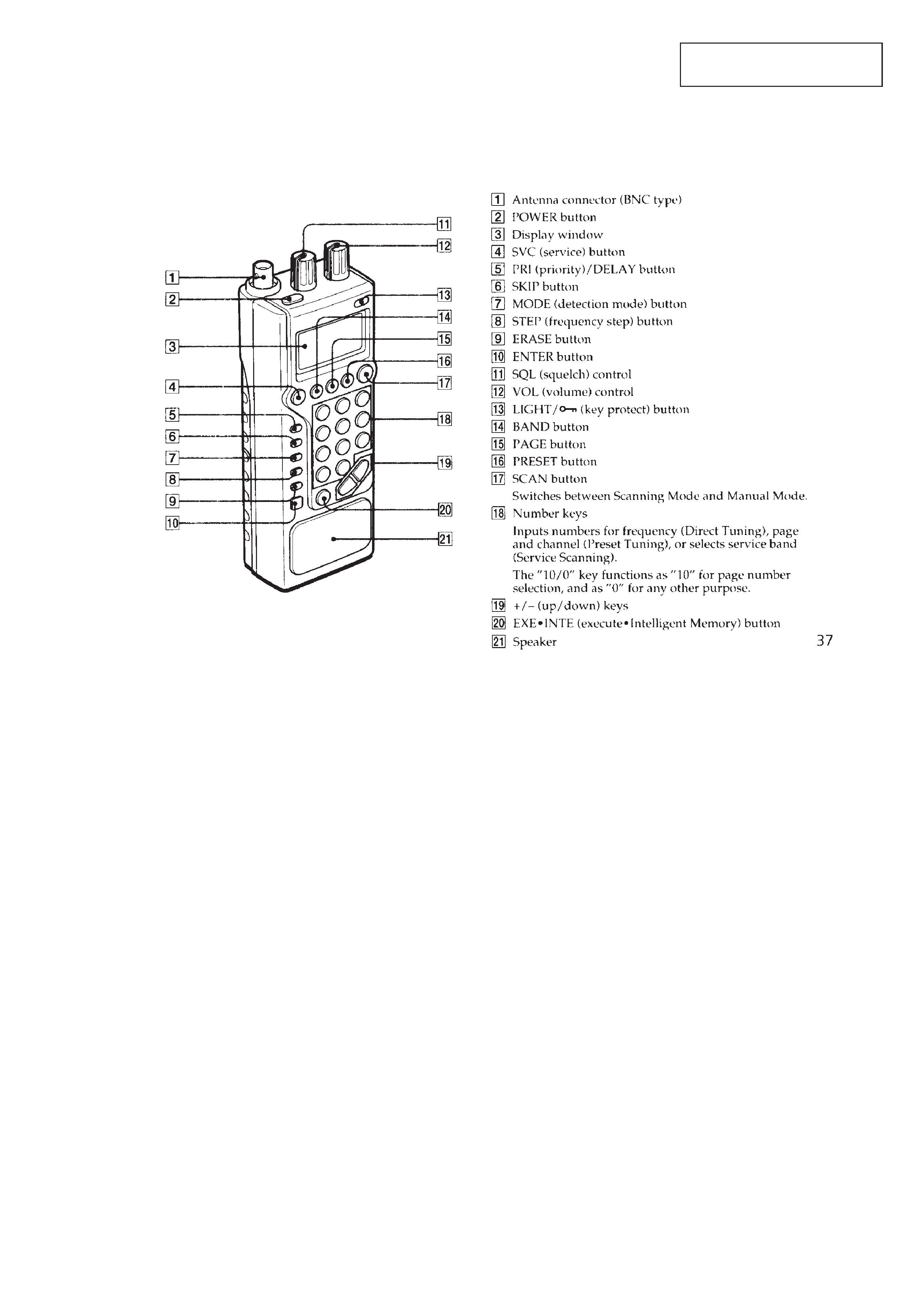
LOCATION AND FUNCTION OF CONTROLS
FRONT
This section is extracted from
instruction manual.
4
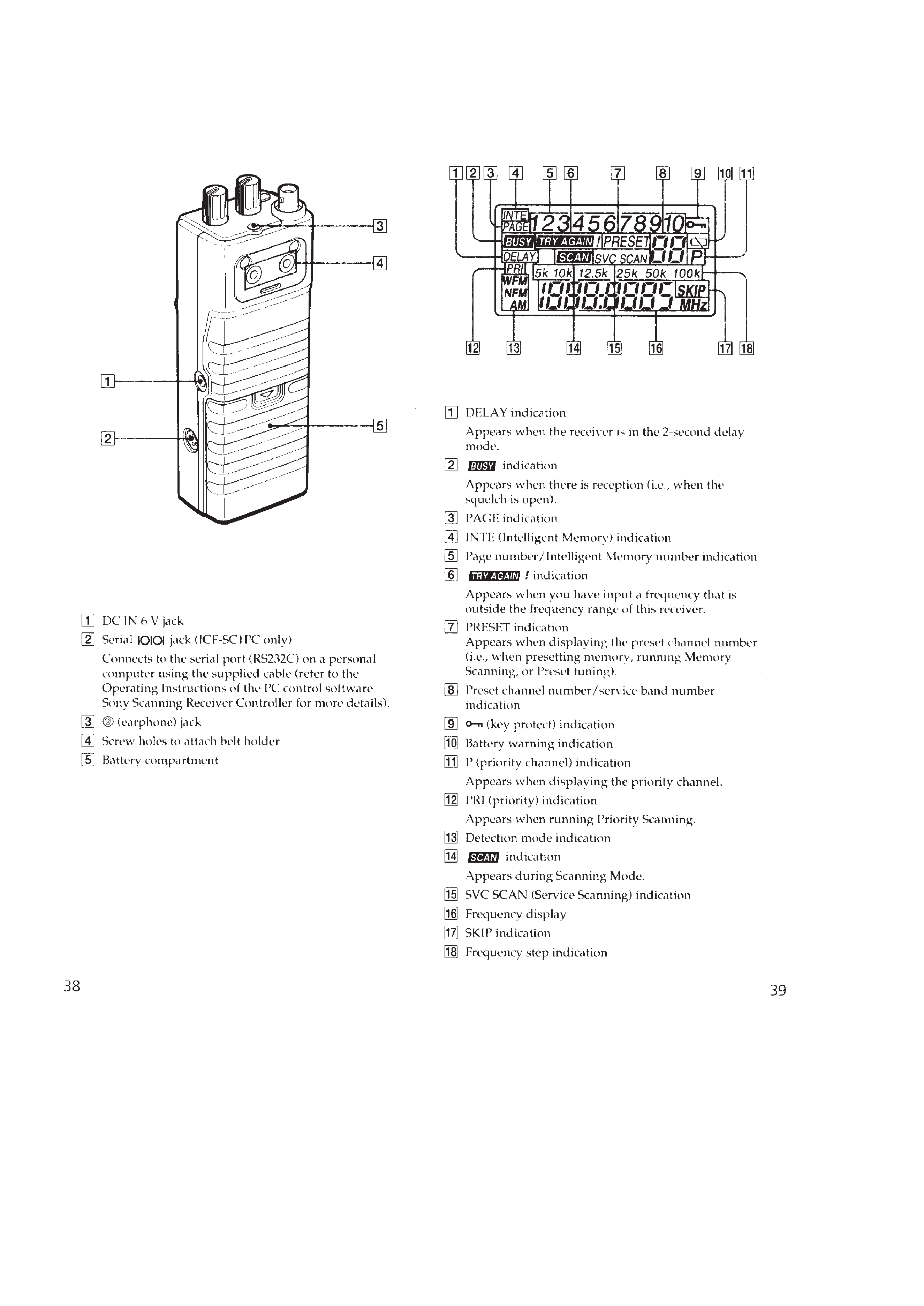
SIDE/REAR
DISPLAY
5