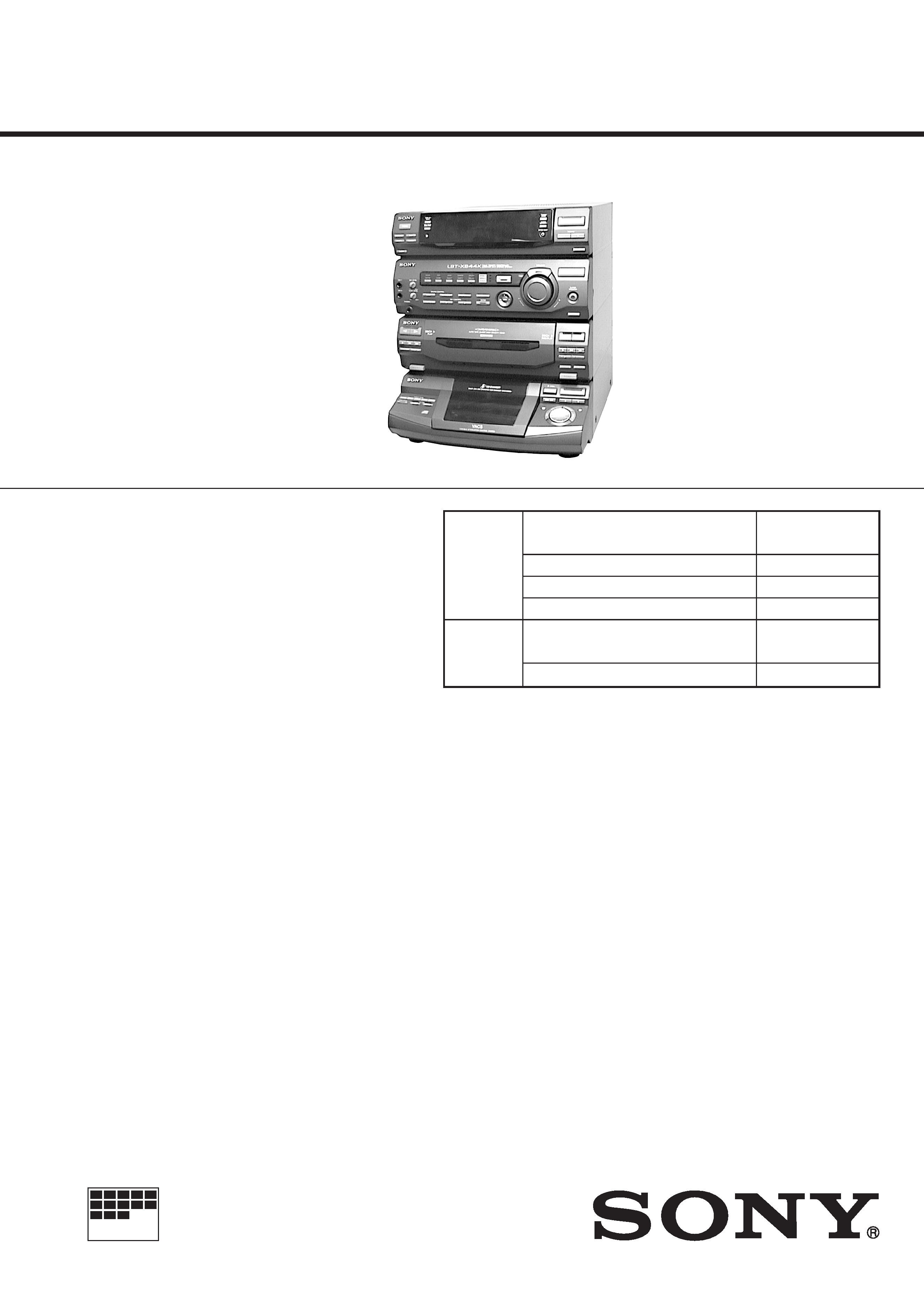
HCD-XB33K/XB44K
SERVICE MANUAL
COMPACT DISC DECK RECEIVER
MICROFILM
Model Name Using Similar Mechanism
HCD-D290/
G3300/XB3
CD Mechanism Type
CDM37L-5BD29AL
Base Unit Name
BU-5BD29AL
Optical Pick-up Name
KSS-213D/Q-NP
Model Name Using Similar Mechanism
HCD-D290/
G3300/XB3
Tape Transport Mechanism Type
TCM-220WR2
-- Continued on next page --
SPECIFICATIONS
E Model
Photo: HCD-XB44K
AUDIO POWER SPECIFICATIONS
POWER OUTPUT AND TOTAL HARMONIC DISTORTION:
With 8 ohm loads, both channels driven, from 70-20,000 Hz; rated 100
watts per channel minimum RMS power, with no more than 0.9 % total
harmonic distortion from 250 milliwatts to rated output.
Amplifier section
(HCD-XB33K)
The following measured at AC 120/240 V, 50 Hz
DIN power output (Rated):
100 + 100 watts (6 ohms at 1 kHz, DIN)
Continuous RMS power output (Reference):
120 + 120 watts
(6 ohms at 1 kHz, 10% THD)
Peak music power potput (Reference):
1,500 watts
(HCD-XB44K)
The following measured at AC 120/240 V, 50 Hz
DIN power output (Rated):
120 + 120 watts (6 ohms at 1 kHz, DIN)
Continuous RMS power output (Reference):
140 + 140 watts
(6 ohms at 1 kHz, 10% THD)
Peak music power output (Reference):
2,000 watts
Inputs
PHONO IN (phono jacks):
sensitivity 3 mV, impedance 47 kilohms
MIX MIC (phone jack):
sensitivity 1 mV, impedance 10 kilohms
VIDEO/MD (AUDIO) IN (phono jacks):
sensitivity 250 mV, impedance 47 kilohms
Outputs
PHONES (stereo phone jack):
accepts headphones of 8 ohms or more
VIDEO/MD (AUDIO) OUT (phono jacks):
voltage 250 mV, impedance 1 kilohm
SPEAKER:
impedance of 6 to 16 ohms
SURROUND SPEAKER: accepts impedance of 16 ohms
(HCD-XB33K)
* Dolby noise reduction manufactured under license
from Dolby Laboratories Licensing Corporation.
"DOLBY" and the double-D symbol a are
trademarks of the Dolby Laboratories Licensing
Corporation.
CD
Section
Tape Deck
Section
CD player section
System
Compact disc and digital audio system
Laser
Semiconductor laser (
= 780nm).
Emission
duration: continuous
Laser output
Max. 44.6µW*
*This output is the value measured at a distance
of 200 mm from the objective lens surface on
the Optical Pick-up Block with 7 mm aperture.
Wavelength
780 790 nm
Frequency response
2 Hz 20 kHz (±0.5 dB)
Signal-to-noise ratio
More than 90 dB
Dynamic range
More than 90 dB
CD DIGITAL OUT
(square optical connector jack, rear panel)
Wave length:
600 nm
Output level:
18 dBm
Tape player section
Recording system
4-track 2-channel stereo
Frequency response (DOLBY NR OFF)
60 13,000 Hz (±3 dB), using a Sony
TYPE I cassette
60 14,000 Hz (±3 dB), using a Sony
TYPE II cassette
Tuner section
FM stereo, FM/AM superheterodyne tuner
FM tuner section
Tuning range
(2 band model)
Antenna
FM wire antenna
Antenna terminals
75 ohm unbalanced
Intermediate frequency
10.7 MHz
AM tuner section
Tuning range
531 1,602 kHz
(with the tuning interval set at 9 kHz)
530 1,710 KHz
(with the tuning interval set at 10 kHz)
Antenna
AM loop antenna, External antenna terminals
Intermediate frequency
450 kHz
General
Power requirements
Other models:
110 120 V or 220 240 V
AC, 50/60 Hz Adjustable with voltage selector
Power consumption
(HCD-XB33K):
240 watts
(HCD-XB44K):
250 watts
Dimensions (w/h/d)
Approx. 355 x 425 x 435 mm (14 x 16 3/4 x 17
1/4 in) incl. projecting parts and controls
Mass
Approx. 14.0 kg (30 lb 14 oz.)
Supplied accessories:
AM loop antenna (1)
Remote RM-SD70S (1)
Size AA (R6) batteries (2)
FM wire antenna (1)
Speaker cords* (HCD-XB44K) (2)
Design and specifications are subject to change without notice.
-- 2 --
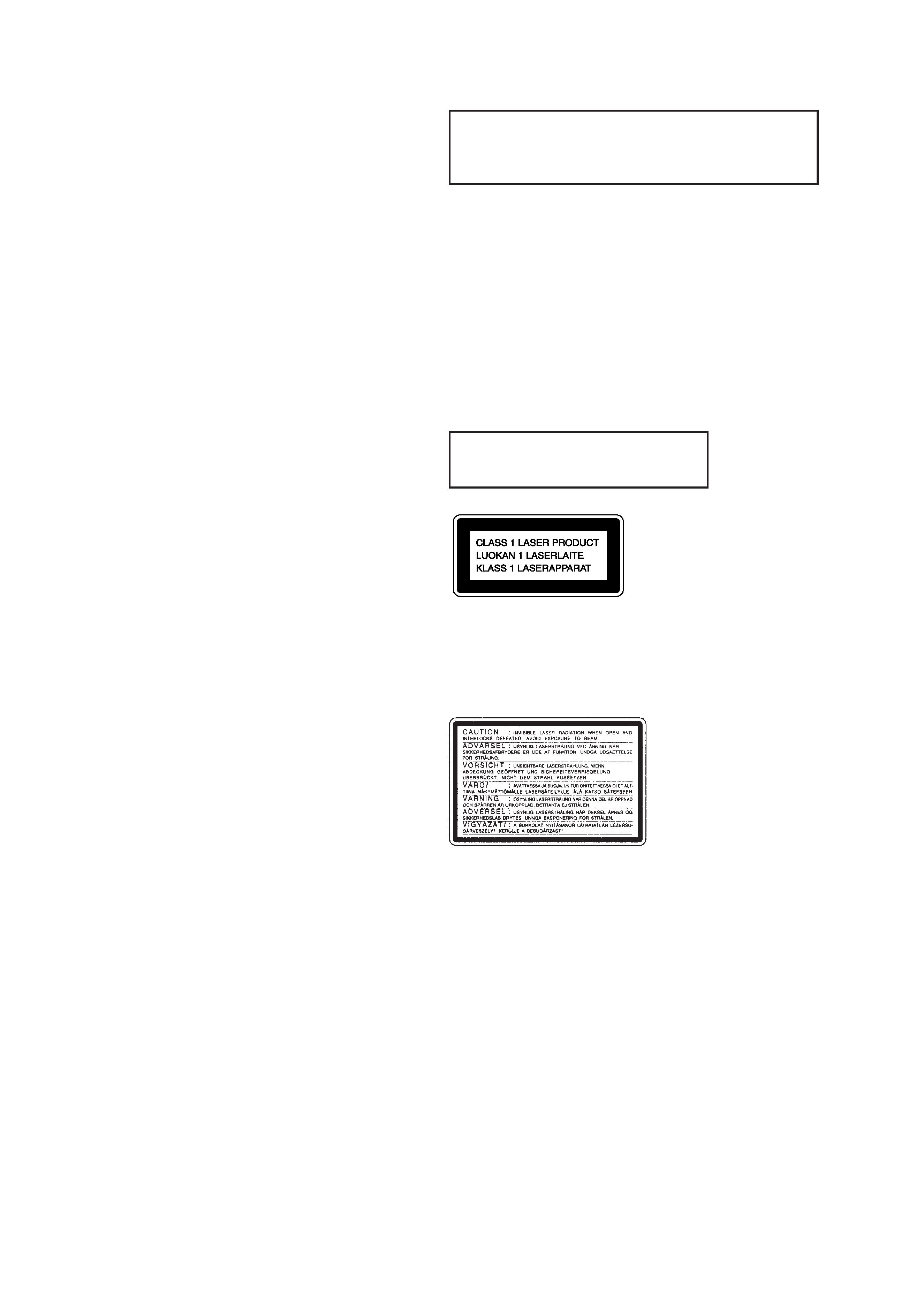
This appliance is classified as a CLASS 1 LASER product. The
CLASS 1 LASER PRODUCT MARKING is located on the rear
exterior.
The following caution label is located inside the unit.
Laser component in this product is capable
of emitting radiation exceeding the limit for
Class 1.
CAUTION
Use of controls or adjustments or performance of procedures
other than those specified herein may result in hazardous radiation
exposure.
Notes on chip component replacement
· Never reuse a disconnected chip component.
· Notice that the minus side of a tantalum capacitor may be
damaged by heat.
Flexible Circuit Board Repairing
· Kee p the temperature of soldering iron around 270°C
during repairing.
· Do not touch the soldering iron on the same conductor of the
circuit board (within 3 times).
· Be careful not to apply force on the conductor when soldering
or unsoldering.
SAFETY-RELATED COMPONENT WARNING!!
COMPONENTS IDENTIFIED BY MARK ! OR DOTTED LINE WITH
MARK ! ON THE SCHEMATIC DIAGRAMS AND IN THE PARTS
LIST ARE CRITICAL TO SAFE OPERATION. REPLACE THESE
COMPONENTS WITH SONY PARTS WHOSE PART NUMBERS
APPEAR AS SHOWN IN THIS MANUAL OR IN SUPPLEMENTS
PUBLISHED BY SONY.

-- 3 --
TABLE OF CONTENTS
1. GENERAL
FRONT PANEL ···························································· 5
BACK PANEL ······························································ 6
2. DISASSEMBLY ····························································· 10
3. TEST MODE ··································································· 18
4. MECHANICAL ADJUSTMENTS ···························· 20
5. ELECTRICAL ADJUSTMENTS
DECK Section ································································· 20
CD Section ······································································· 23
6. DIAGRAMS
6-1.
Circuit Board Location ···················································· 25
6-2.
Block Diagrams
CD/Key Control Section ············································ 26
Main Section ······························································ 27
6-3.
Printed Wiring Board BD Section ····························· 31
6-4
Schematic Diagram BD Section ································ 33
6-5.
Printed Wiring Board CD Motor Section ················· 35
6-6.
Schematic Diagram CD Motor Section ···················· 37
6-7.
Printed Wiring Board Deck Section ························· 39
6-8.
Schematic Diagram Deck Section ···························· 41
6-9.
Schematic Diagram Switch Section ·························· 43
6-10. Printed Wiring Board Switch Section ······················· 45
6-11. Printed Wiring Board Headphone-Mic Section ········ 46
6-12. Schematic Diagram Headphone-Mic Section ··········· 47
6-13. Printed Wiring Board Panel Section ························· 49
6-14. Schematic Diagram Panel Section ····························· 51
6-15. Printed Wiring Board Power Section ························· 53
6-16. Schematic Diagram Power Section ··························· 55
6-17. Printed Wiring Board Main Section ························· 57
6-18. Schematic Diagram Main Section (1/5) ···················· 59
6-19. Schematic Diagram Main Section (2/5) ···················· 61
6-20. Schematic Diagram Main Section (3/5) ···················· 63
6-21. Schematic Diagram Main Section (4/5) ···················· 65
6-22. Schematic Diagram Main Section (5/5) ···················· 67
6-23. Schematic Diagram Key Control Section ·················· 69
6-24. Printed Wiring Board Key Control Section ··············· 69
6-25. IC Block Diagrams ·························································· 71
6-26. IC Pin Function Description ············································ 76
7. EXPLODED VIEWS ····················································· 79
8. ELECTRICAL PARTS LIST ······································ 88
-- 4 --
SERVICING NOTES
The laser diode in the optical pick-up block may suffer electrostatic
break-down because of the potential difference generated by the
charged electrostatic load, etc. on clothing and the human body.
During repair, pay attention to electrostatic break-down and also
use the procedure in the printed matter which is included in the
repair parts.
The flexible board is easily damaged and should be handled with
care.
NOTES ON LASER DIODE EMISSION CHECK
The laser beam on this model is concentrated so as to be focused on
the disc reflective surface by the objective lens in the optical pick-
up block. Therefore, when checking the laser diode emission,
observe from more than 30 cm away from the objective lens.
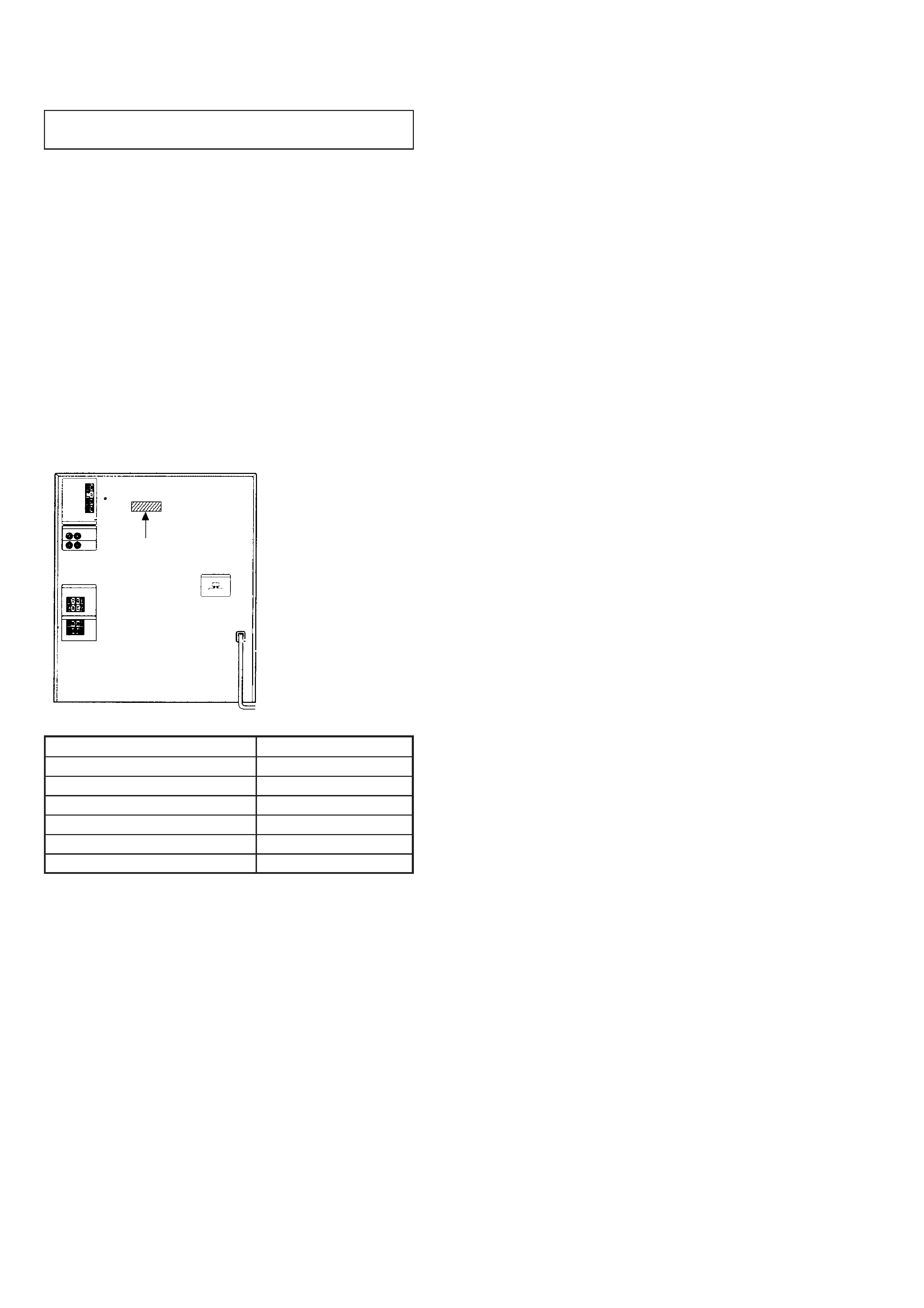
MODEL IDENTIFICATION
BACK PANEL
NOTES ON HANDLING THE OPTICAL PICK-UP
BLOCK OR BASE UNIT
PARTS No.
MODEL
PARTS No.
XB33K: SP, MY model
4-996-410-1
XB33K: E model
4-996-410-6
XB33K: EA model
4-996-410-7
XB44K: SP, MY model
4-996-412-1
XB44K: E, IA model
4-996-412-6
XB44K: EA model
4-996-412-7
-- 5 --
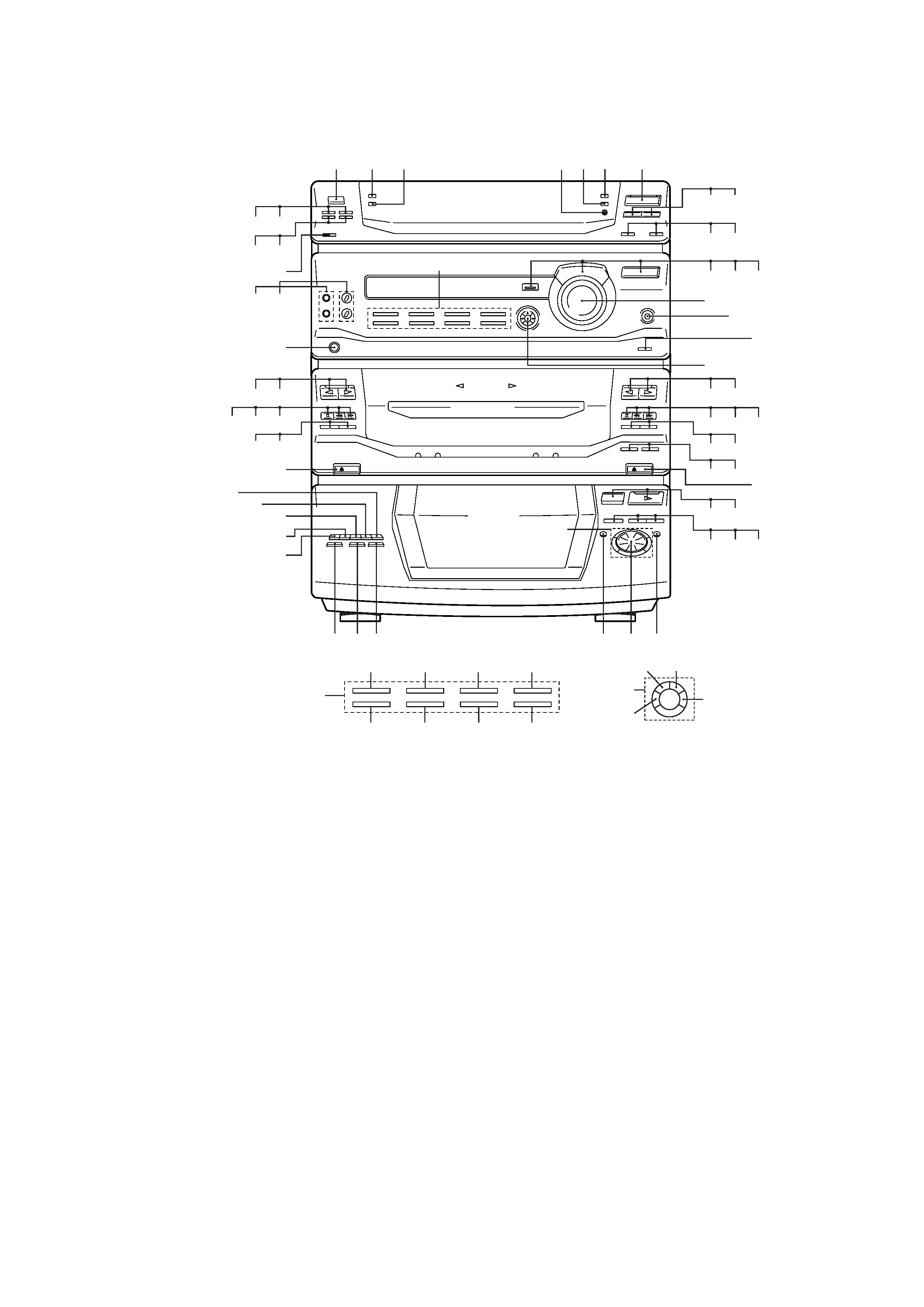
FRONT PANEL
SECTION 1
GENERAL
12
3
4
6
7
89
%ª ^º
%¶ %·
%§
5
!º !¡
!TM
!
!·
!£ !¢
@¡ @TM @£
#¡ #TM #£
#¢
&TM
^ª
&º
&¡
^¡
^TM
^£
^¢
^·
^
#
#§
#· #¶
#ª
B
B
A
!ª @º
@¢ @
!§
!¶
@·
@§ @¶
@ª #º
see B
^¶
^§
%¢ %
%£
%¡ %TM
$§
$£
$¢
$º
$¶
$
$TM
$¡
$ª
$·
%º
A
see A
1
POWER button
2
DISPLAY/DEMO button
3
SPECTRUM ANALYZER button
4
ENTER/NEXT button
5
TUNER MEMORY button
6
TUNING MODE button
7
TUNER/BAND button
8
TUNING button
9
TUNING + button
!º
PTY button (AEP, UK model)
!¡
STEREO/MONO button
!TM
EFFECT button
!£
GROOVE button
!¢
FUNCTION button
!
VOLUME knob
!§
SUPER WOOFER button
!¶
SUPER W MODE (XB44K model)
!·
GEQ button
!ª
DECK B ª (play) button
@º
DECK B · (play) button
@¡
DECK B p (stop) button
@TM
DECK B 0 (backward) button
@£
DECK B ) (forward) button
@¢
DECK B P (pause) button
@
DECK B r REC button
@§
H SPEED DUB button
@¶
CD SYNC button
@·
DECK B 6 EJECT button
@ª
CD 6 OPEN button
#º
CD · (play) button
#¡
DISK SKIP button
#TM
CD P (pause) button
#£
CD p (stop) button
#¢
CD ) (forward) button
#
AMS ± knob
#§
CD 0 (backward) button
#¶
FLASH button
#·
LOOP button
#ª
NON-STOP button
$º
DISC 1 button
$¡
DISC 2 button
$TM
DISC 3 button
$£
DISC 4 button
$¢
DISC 5 button
$
DECK A 6 EJECT button
$§
DIRECTION button
$¶
DOLBY NR button
$·
DECK A p (stop) button
$ª
DECK A 0 (backward) button
%º
DECK A ) (forward) button
%¡
DECK A ª (play) button
%TM
DECK A · (play) button
%£
PHONES jack
%¢
MIC1, MIC2 jack
%
MIC LEVEL, ECHO LEVEL knob
%§
SLEEP button
%¶
DAILY 1 button
%·
DAILY 2 button
%ª
t / CLOCK SET button
^º
REC button
^¡
WAVE button
^TM
SURROUND button
^£
P FILE MEMORY button
^¢
GEQ CONTROL button
^
ENTER button
^§
KEY CONTROL (n) button
^¶
KEY CONTROL (~) button
^·
KARAOKE PON/MPX button
^ª
PLAY MODE button
&º
REPEAT button
&¡
EDIT button
&TM
1/ALL DISCS button