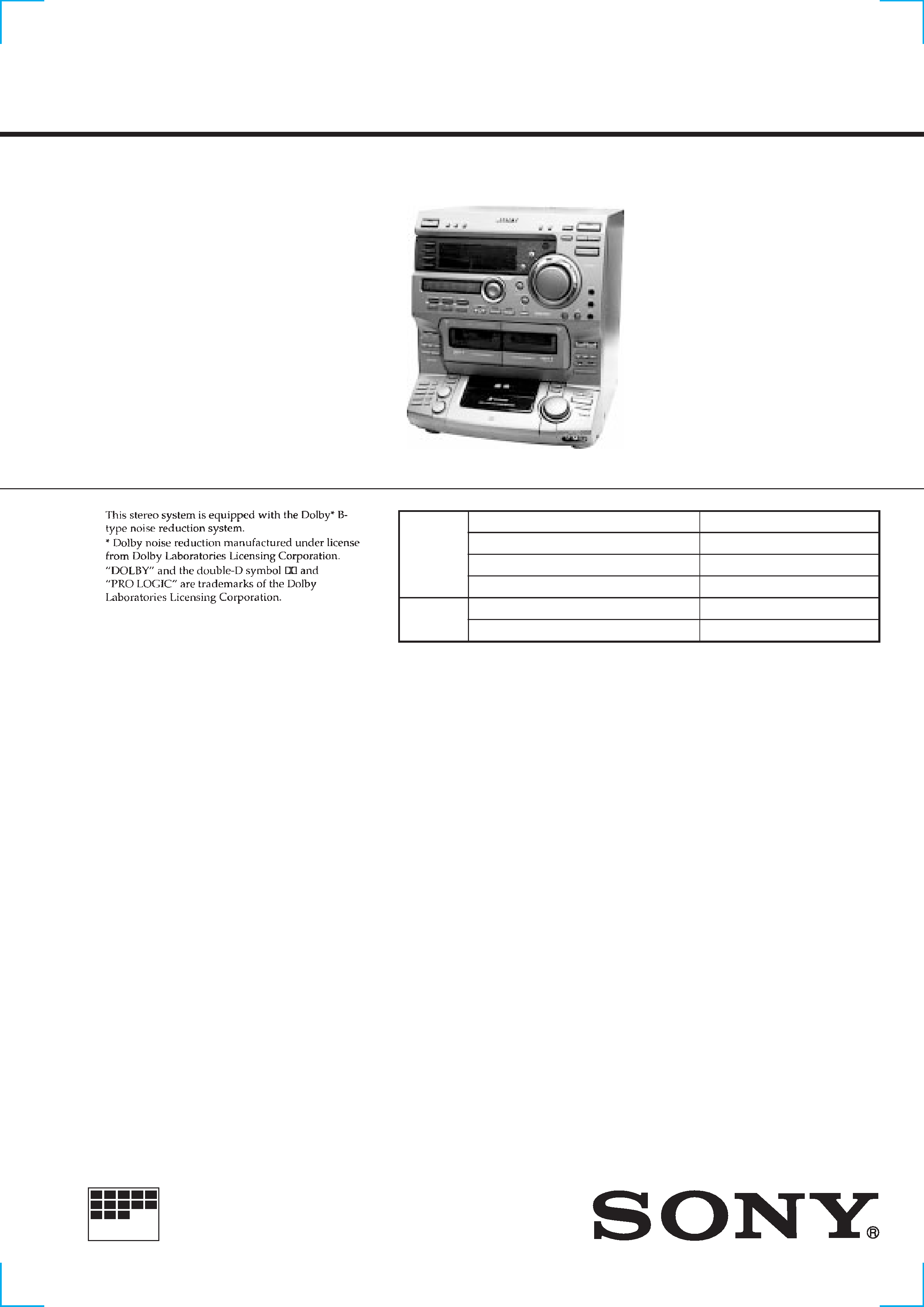
HCD-VR90AV
E Model
SERVICE MANUAL
COMPACT Hi-Fi STEREO SYSTEM
MICROFILM
SPECIFICATIONS
HCD-VR90AV is the tuner, deck, CD and ampli-
fier section in LBT-VR90AV.
Model Name Using Similar Mechanism
HCD-VR50/VR70
CD Mechanism Type
CDM37L-5BD34L
Base Unit Name
BU-5BD34L
Optical Pick-up Name
KSS-213D/Q-NP
Model Name Using Similar Mechanism
NEW
Tape Transport Mechanism Type
TCM-230AWR2/230PWR2
CD
Section
Tape deck
Section
Amplifier section
Front Speaker:
The following measured at AC 120/220/240V, 50/60Hz
DIN power output (Rated)
130 + 130W
(6
at 1 kHz, DIN)
Continuous RMS power output (Reference)
160 +160W
(6
at 1 kHz, 10% THD)
Center Speaker:
DIN power output (Rated)
30W
(8
at 1 kHz, DIN)
Continuous RMS power output (Reference)
40W
(8
at 1 kHz, 10% THD)
Rear Speaker:
DIN power output (Rated)
30 + 30W
(8
at 1 kHz, DIN)
Continuous RMS power output (Reference)
40 + 40W
(8
at 1 kHz, 10% THD)
Inputs
PHONO IN (phono jacks):
sensitivity 3mV,
impedance 47k
MIX MIC (phone jack):
sensitivity 1mV,
impedance 10k
VIDEO1 IN (phono jacks):
sensitivity 250mV,
impedance 47k
VIDEO2 IN (phono jacks):
sensitivity 250mV,
impedance 47k
MD IN (phono jacks):
sensitivity 450mV,
impedance 47k
DVD INPUT
FRONT (phono jacks):
sensitivity 450mV,
impedance 47k
REAR (phono jacks):
sensitivity 450mV,
impedance 47k
CENTER (phono jacks):
sensitivity 450mV,
impedance 47k
WOOFER (phono jacks):
sensitivity 450mV,
impedance 47k
Outputs
PHONES (stereo phone jack):
accepts headphones of
8
or more
VIDEO OUT (phono jack):
voltage 250mV,
impedance 1k
MD OUT (phono jacks):
voltage 250mV,
impedance 1k
WOOFER OUT (phono jack):
voltage 1V,
impedance 1k
FRONT SPEAKER:
accepts impedance of 8
to 16
CENTER SPEAKER:
accepts impedance of 8
to 16
REAR SPEAKER:
accepts impedance of 8
to 16
-- Continued on next page --
Video section
Inputs
VIDEO1 IN (phono jacks):
1Vp-p, 75
VIDEO2 IN (phono jacks):
1Vp-p, 75
DVD INPUT VIDEO (phono jacks):
1Vp-p, 75
Output
VIDEO OUT (phono jack):
1Vp-p, 75
S-VIDEO OUT (4-pin/mini-DIN jack):
Y : 1Vp-p, unbalanced,
Sync negative,
C : 0.286 V p-p,
load immpedance
75

2
VIDEO CD/CD player section
System
Compact disc and digital audio and video system
Laser
Semiconductor laser
(
=780nm) Emission
duration: continuous
Laser output
Max. 44.6µW*
* This output is the value measured at a distance of
200 mm from the objective lens surface on the Optical
Pick-up Block with 7 mm aperture.
Wave length
780 790 nm
Frequency response
2Hz 20kHz (±0.5dB)
Signal-to-noise ratio
More than 90 dB
Dynamic range
More than 90 dB
Video color system format
NTSC, PAL
CD DIGITAL OUT
(square optical connector jack, rear panel)
Wave length:
660 nm
Output level:
18dBm
Tape player section
Recording system
4-track 2-channel stereo
Frequency response (DOLBY NR OFF)
40 13,000Hz (±3dB),
using a Sony TYPE I
cassette
40 14,000Hz (±3dB),
using a Sony TYPE II
cassette
Wow and flutter
±0.15% W.Peak (IEC)
0.1% W.RMS (NAB)
±0.2% W.Peak (DIN)
Tuner section
FM stereo, FM/AM superheterodyne tuner
FM tuner section
Tuning range
87.5 108.0 kHz
(100 kHz step)
Antenna
FM wire antenna
Antenna terminals
75
unbalanced
Intermediate frequency 10.7 MHz
AM tuner section
Tuning range
Middle Eastern model : 531 1,602 kHz
(with the tuning interval set at 9 kHz)
Other models :
531 1,602 kHz
(with the tuning interval set at 9 kHz)
530 1,710 kHz
(with the tuning interval set at 10 kHz)
Antenna
AM loop antenna, External antenna terminals
Intermediate frequency 450 kHz
General
Power requirements
Thai model :
220 V AC, 50/60 Hz
Other models :
120 V, 220V, or 230 240 V AC, 50/60 Hz
Adjustable with voltage selector
Power consumption
280 W
Dimensions (w/h/d)
Approx. 356
× 423 × 446 mm
incl. projecting parts and controls
Mass
Approx. 15.0 kg
Supplied accessories
AM loop antenna (1)
Remote RM-SV100AVB (1)
R6 (size AA) batteries (2)
FM wire antenna (1)
Speaker cords (2)
Video connecting cable
Design and specifications are subject to change without notice.
3
SAFETY-RELATED COMPONENT WARNING!!
COMPONENTS IDENTIFIED BY MARK
! OR DOTTED LINE WITH
MARK
! ON THE SCHEMATIC DIAGRAMS AND IN THE PARTS
LIST ARE CRITICAL TO SAFE OPERATION. REPLACE THESE
COMPONENTS WITH SONY PARTS WHOSE PART NUMBERS
APPEAR AS SHOWN IN THIS MANUAL OR IN SUPPLEMENTS
PUBLISHED BY SONY.
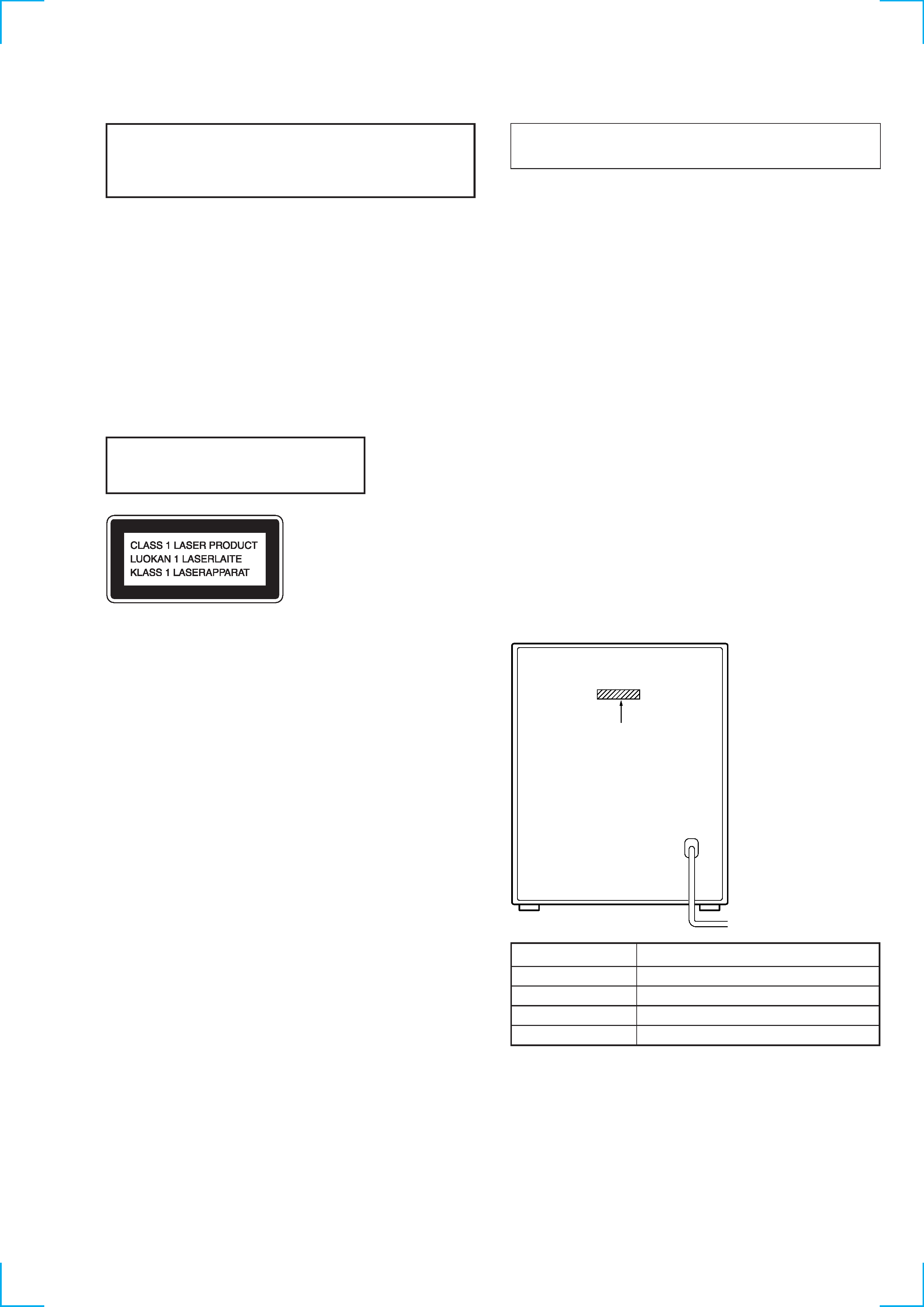
This appliance is classified as a CLASS 1 LASER product. The
CLASS 1 LASER PRODUCT MARKING is located on the rear
exterior.
The following caution label is located inside the unit.
Laser component in this product is capable
of emitting radiation exceeding the limit for
Class 1.
CAUTION
Use of controls or adjustments or performance of procedures
other than those specified herein may result in hazardous radiation
exposure.
Notes on chip component replacement
· Never reuse a disconnected chip component.
· Notice that the minus side of a tantalum capacitor may be
damaged by heat.
Flexible Circuit Board Repairing
· Keep the temperature of soldering iron around 270°C
during repairing.
· Do not touch the soldering iron on the same conductor of the
circuit board (within 3 times).
· Be careful not to apply force on the conductor when soldering
or unsoldering.
MODEL IDENTIFICATION
-- BACK PANEL --
· Abbreviation
IA
: Indonesia model
EA
: Saudi Arabia model
MY
: Malaysia model
SP
: Singapore model
TH
: Thai model
Parts No.
NOTES ON HANDLING THE OPTICAL PICK-UP BLOCK
OR BASE UNIT
The laser diode in the optical pick-up block may suffer electrostatic
break-down because of the potential difference generated by the
charged electrostatic load, etc. on clothing and the human body.
During repair, pay attention to electrostatic break-down and also
use the procedure in the printed matter which is included in the
repair parts.
The flexible board is easily damaged and should be handled with
care.
NOTES ON LASER DIODE EMISSION CHECK
The laser beam on this model is concentrated so as to be focused on
the disc reflective surface by the objective lens in the optical pick-
up block. Therefore, when checking the laser diode emission,
observe from more than 30 cm away from the objective lens.
LASER DIODE AND FOCUS SEARCH OPERATION
CHECK
Carry out the "S curve check" in "CD section adjustment" and check
that the S curve waveform is output four times.
PARTS No.
MODEL
4-214-793-0
MY,SP
4-214-793-1
EA
4-214-793-3
IA
4-214-793-4
TH

4
TABLE OF CONTENTS
6-15. Schematic Diagram
Deck Section ································ 40
6-16. Printed Wiring Board
Deck Section ····························· 41
6-17. Printed Wiring Board
Power Section ··························· 42
6-18. Schematic Diagram
Power (1/2) Section ····················· 43
6-19. Schematic Diagram
Power (2/2) Section ····················· 44
6-20. Schematic Diagram
Surround Section ························· 45
6-21. Printed Wiring Board
Surround Section ······················· 45
6-22. Schematic Diagram
FL Section ···································· 46
6-23. Printed Wiring Board
FL Section ································· 47
6-24. Schematic Diagram
Panel VR Section ························· 48
6-25. Printed Wiring Board
Panel VR Section ······················ 49
6-26. Schematic Diagram
TC Panel Section ························· 50
6-27. Printed Wiring Board
TC Panel Section ······················· 51
6-28. Schematic Diagram
CD Panel Section ························· 52
6-29. Printed Wiring Board
CD Panel Section ······················ 53
6-30. Schematic Diagram
CD Motor Section ························ 54
6-31. Printed Wiring Board
CD Motor Section ····················· 55
6-32. Schematic Diagram
Jack Section ································· 56
6-33. Printed Wiring Board
Jack Section ······························ 57
6-34. Schematic Diagram
Trans Section ······························· 58
6-35. Printed Wiring Board
Trans Section ····························· 59
6-36. Schematic Diagram
Leaf SW Section ·························· 59
6-37. Printed Wiring Board
Leaf SW Section ······················· 59
6-38. IC Block Diagrams ··························································· 60
6-39. IC Pin Functions ······························································· 61
7. EXPLODED VIEWS
7-1.
Case and Back Panel Section ··········································· 69
7-2.
Front Panel Section 1 ······················································· 70
7-3.
Front Panel Section 2 ······················································· 71
7-4.
Chassis Section ································································· 72
7-5.
TC Mechanism Section 1 (TCM230AWR2/230PWR2) ·· 73
7-6.
TC Mechanism Section 2 (TCM230AWR2/230PWR2) ·· 74
7-7.
CD Mechanism Section (CDM37M-5BD32L) ················ 75
7-8.
Base Unit Section (BU-5BD32L) ····································· 76
8. ELECTRICAL PARTS LIST ······································· 77
1. GENERAL ·········································································· 5
2. DISASSEMBLY
2-1.
Front Panel ········································································· 7
2-2.
Main Board ········································································· 7
2-3.
Sub Panel ············································································ 8
2-4.
CD-L/CD-R Board and CD Lid Assembly ························· 8
2-5.
Tape Mechanism Deck and Cassette Lid ···························· 9
2-6.
CD Mechanism Deck ························································· 9
2-7.
Base Unit ············································································ 9
2-8.
Disc Table ········································································· 10
3. SERVICE MODE ···························································· 11
4. MECHANICAL ADJUSTMENTS ····························· 15
5. ELECTRICAL ADJUSTMENTS ······························· 15
6. DIAGRAMS
6-1.
Circuit Boards Location ··················································· 19
6-2.
Block Diagrams
BD Section ······································································· 20
Video Section ··································································· 21
Deck Section ····································································· 22
Main (1/2) Section ···························································· 23
Main (2/2) Section ···························································· 24
Power Section ··································································· 25
Display Section ································································· 26
6-3.
Printed Wiring Board
BD Section ································ 28
6-4.
Schematic Diagram
BD Section ··································· 29
6-5.
Printed Wiring Board
Video Section ···························· 30
6-6.
Schematic Diagram
Video (1/3) Section ······················ 31
6-7.
Schematic Diagram
Video (2/3) Section ······················ 32
6-8.
Schematic Diagram
Video (3/3) Section ······················ 33
6-9.
Printed Wiring Board
Main Section ····························· 34
6-10. Schematic Diagram
Main (1/5) Section ······················· 35
6-11. Schematic Diagram
Main (2/5) Section ······················· 36
6-12. Schematic Diagram
Main (3/5) Section ······················· 37
6-13. Schematic Diagram
Main (4/5) Section ······················· 38
6-14. Schematic Diagram
Main (5/5) Section ······················· 39
5
SECTION 1
GENERAL
Location of Parts and Controls
1 1/u (Power) button
2 POWER SAVE/DEMO (STANDBY)
button
3 DISPLAY button
4 SPECTRUM ANALYZER button
5 Display window
6 GEQ control button
7 SYNC BASS button
8 SYNC EQ button
9 Remote sensor
0 TUNING MODE button
!¡ STEREO/MONO button
!TM ENTER/NEXT button
!£ TUNER MEMORY button
!¢ TUNER/BAND button
! TUNING - button
!§ TUNING + button
!¶ FUNCTION button
!· VOLUME knob
!ª PHONES jack
@º ECHO LEVEL knob
@¡ MIC LEVEL knob
@TM MIC 1 jack
@£ MIC 2 jack
@¢ GROOVE button
@ SUPER WOOFER button
@§ MODE button
@¶ ª (B Deck) button and indicator
@· · (B Deck) button and indicator
@ª p (B Deck) button
#º 0 (B Deck) button
#¡ ) (B Deck) button
#TM P (B Deck) button
#£ r REC (B Deck) button
#¢ HI-SPEED DUB button
# CD SYNCHRO button
#§ PLAY MODE button
#¶ REPEAT button
#· 0 (CD) button
#ª ) (CD) button
$º ·P (CD) button and indicator
$¡ p (CD) button
$TM DISC SKIP button
$£ = AMS + knob
$¢ VIDEO2 INPUT jacks
$ PRO LOGIC button and indicator
$§ DVD 5.1 CH
$¶ KEY CONTROL # button
$· KEY CONTROL b button
$ª EDIT button
%º NON-STOP button and indicator
%¡ FLASH button
%TM LOOP button
%£ NEXT button
%¢ PREV button
% RETURN button
%§ DISC 5 button
%¶ DISC 4 button
%· DISC 3 button
%ª DISC 2 button
^º DISC 1 button
^¡ SELECT button
^TM ACTIVE button
^£ DOLBY NR button
^¢ DIRECTION button
^ ) (A Deck) button
^§ 0 (A Deck) button
^¶ p (A Deck) button
^· · (A Deck) button
^ª ª (A Deck) button
&º KARAOKE PON/MPX button
&¡ DSP button and indicator
&TM EFFECT button and indicator
&£ ENTER button and indicator
&¢ GEQ CONTROL button
& P. FILE MEMORY
&§ Equalizer indicators
&¶ t/CLOCK SET button
&· SLEEP button
&ª REC button and indicator
*º DAILY button and indicator
· AMS is the abbreviation for Automatic
Music Sensor.
Front Panel
234
1
@·
#¡
#º
@ª
@¶
#ª
#·
^£
^¢
&º
&¡
&TM
&£
&¢
&
^
^§
^¶
^·
^ª
#TM#£
#¢ #
$º
$TM
$¢
$£
#¶
#§
$
$§
$¶
$·
$ª
%º
%¡
%£%TM
%
%¢
%§
%·
^º
^TM
&¶
%¶
&·
&ª
*º
%ª
^¡
$¡
@¡
!·
@¢
@
@§
@º
!ª
!¶
9
!§
@TM
@£
!
56
7 8
0!¡
!£
!TM
!¢
&§