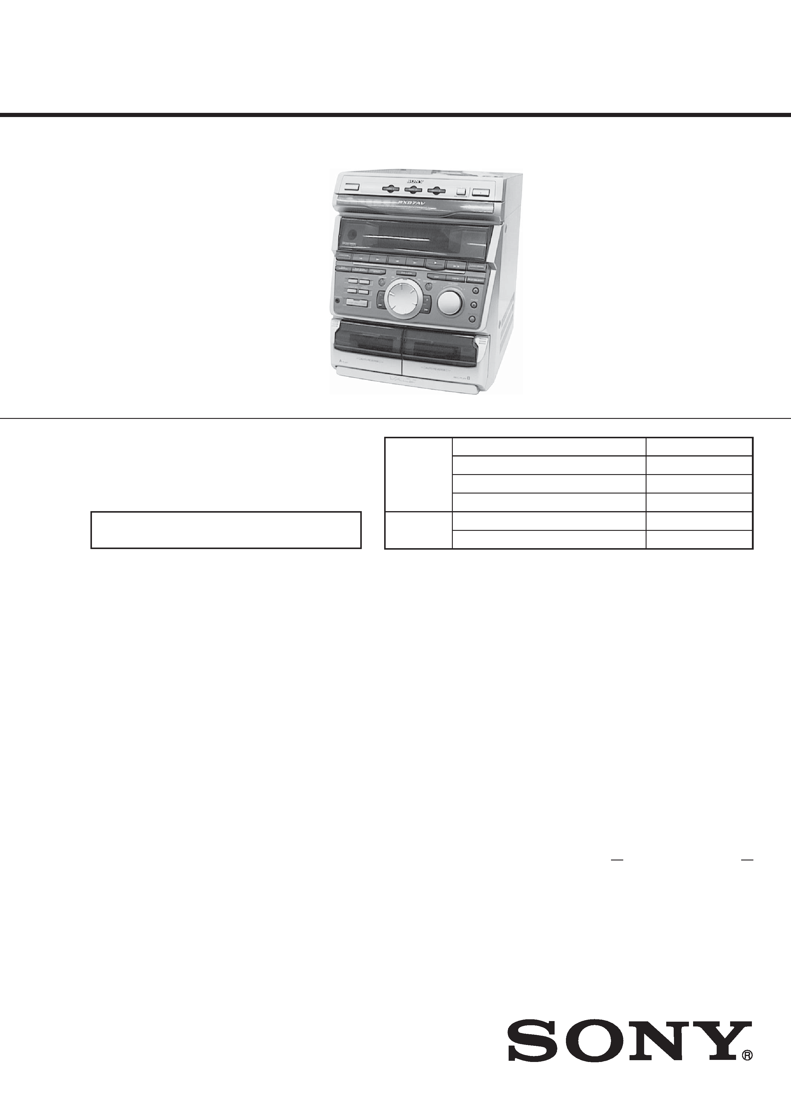
HCD-RXD7AV
US Model
Canadian Model
SERVICE MANUAL
MINI Hi-Fi COMPONENT SYSTEM
Manufactured under license from Dolby Laboratories
Licensing Corporation.
"DOLBY" and the double-D symbol
aare trademarks
of Dolby Laboratories Licensing Corporation.
Model Name Using Similar Mechanism HCD-RXD3
CD
CD Mechanism Type
CX3
Section
Base Unit Name
KSM-213ECM
Optical Pick-up Name
KSS-213ECM/C2NP
Tape deck
Model Name Using Similar Mechanism HCD-RXD6
Section
Tape Transport Mechanism Type
CWL-44-RR
U.S and foreign patents licensed from Dolby
Laboratories Licensing Corporation.
SPECIFICATIONS
HCD-RXD7AV is the Amplifier, CD
player, Tape Deck and Tuner section in
MHC-RXD7AV.
Ver 1.1 2002. 03
Sony Corporation
Home Audio Company
Published by Sony Engineering Corporation
9-928-974-12
2002C1600-1
© 2002.03
AUDIO POWER SPECIFICATIONS:
US model
POWER OUTPUT AND TOTAL
HARMONIC DISTORTION :
with 6
loads, both channels driven, from 70 - 20,000
Hz; rates 60 W per channel minimum RMS power,
with no more than 0.9% total harmonic distortion from
250 mW to rated output.
Amplifier section
Front Speaker :
Continuous RMS power output (reference)
70 + 70 W
(6
at 1 kHz, 10% THD)
Total harmonic distortion less than 0.07%
(6
at 1 kHz, 35 W)
Center Surround Speaker :
Continuous RMS power output (reference)
30 W
(6
at 1 kHz, 1% THD)
Rear Surround Speaker :
Continuous RMS power output (reference)
30 + 30 W
(6
at 1 kHz, 1% THD)
Inputs
MD/VIDEO IN :
voltage 450/250 mV,
(phono jacks)
inpedance 47 k
DVD INPUT
FRONT IN :
voltage 450 mV,
(phono jacks)
inpedance 47 k
CENTER IN :
voltage 450 mV,
(phono jacks)
inpedance 47 k
REAR IN :
voltage 450 mV,
(phono jacks)
inpedance 47 k
WOOFER IN :
voltage 450 mV,
(phono jacks)
inpedance 47 k
Outputs
MD/VIDEO OUT :
voltage 250 mV
(phono jacks)
impedance 1 k
PHONES :
accepts headphones of
(stereo phone jack)
8
or more
FRONT SPEAKER : accepts impedance of
6 to 16
or more
CENTER SPEAKER: accepts impedance of
6 to 16
or more
SUPER WOOFER : Voltage 1 V, impedance
1 k
CD player section
System
Compact disc and digital audio
system
Laser
Semiconductor laser (
=780nm)
Emission duration: continuous
Laser output
Max. 44.6 µW*
*This output is the value
measured at a distance of 200
mm from the objective lens
surface on the Optical Pick-up
Block with 7 mm aperture.
Frequency response
20 Hz - 20 kHz (±0.5 dB)
Wavelength
780 -790 nm
Signal-to-noise ratio
More than 90 dB
Dynamic range
More than 90 dB
CD DIGITAL OUT
(Square optical connector jack, rear panel)
Wavelength
600 nm
Output Level
18 dBm
Continued on next page
2
Tape player section
Recording system
4-track 2-channel stereo
Frequency response
60 - 13,000 Hz (±3 dB),
(DOLBY NR OFF)
using Sony TYPE I cassette
Wow and flutter
±0.15% W.Peak (IEC)
0.1% W.RMS (NAB)
±0.2% W.Peak (DIN)
Tuner section
FM stereo, FM/AM superheterodyne tuner
FM tuner section
Tuning range
87.5 - 108.0 MHz
Antenna
FM lead antenna
Antenna terminals
75
unbalanced
Intermediate frequency 10.7 MHz
AM tuner section
Tuning range
530 - 1,710 kHz
Antenna
AM loop antenna
Antenna terminals
External antenna terminal
Intermediate frequency 450 kHz
General
Power requirements
120 V AC, 60 Hz
Power consumption
190 W
Dimensions (w/h/d)
Approx. 280
× 340 × 390 mm
(111/8
× 131/2 × 153/8 in.)
Mass:
Approx. 9.6 kg
(21 lb 2 oz.)
Supplied accessories:
AM loop antenna (1)
Remote (1)
FM lead antenna (1)
Speaker cords (2)
Center speaker pads (4)
Design and specifications are subject to change without notice.
SAFETY-RELATED COMPONENT WARNING!!
COMPONENTS IDENTIFIED BY MARK
! OR DOTTED LINE WITH
MARK
! ON THE SCHEMATIC DIAGRAMS AND IN THE PARTS
LIST ARE CRITICAL TO SAFE OPERATION. REPLACE THESE
COMPONENTS WITH SONY PARTS WHOSE PART NUMBERS
APPEAR AS SHOWN IN THIS MANUAL OR IN SUPPLEMENTS
PUBLISHED BY SONY.
SAFETY CHECK-OUT
(US model only)
After correcting the original service problem, perform the
following safety checks before releasing the set to the customer:
Check the antenna terminals, metal trim, "metallized" knobs, screws,
and all other exposed metal parts for AC leakage. Check leakage as
described below.
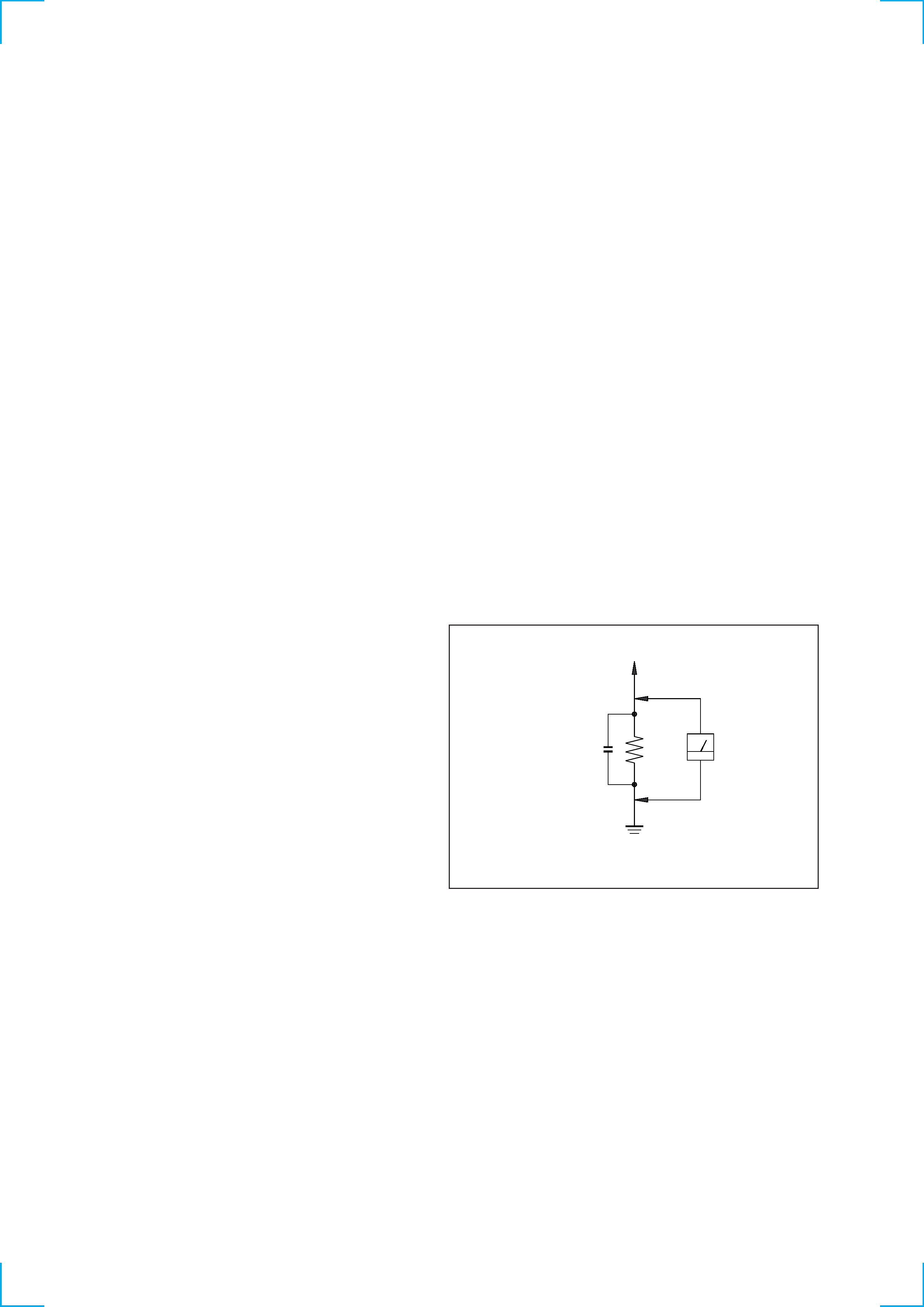
LEAKAGE
The AC leakage from any exposed metal part to earth ground and
from all exposed metal parts to any exposed metal part having a
return to chassis, must not exceed 0.5 mA (500 microampers).
Leakage current can be measured by any one of three methods.
1.
A commercial leakage tester, such as the Simpson 229 or RCA
WT-540A. Follow the manufacturers' instructions to use these
instruments.
2.
A battery-operated AC milliammeter. The Data Precision 245
digital multimeter is suitable for this job.
3.
Measuring the voltage drop across a resistor by means of a
VOM or battery-operated AC voltmeter. The "limit" indication
is 0.75 V, so analog meters must have an accurate low-voltage
scale. The Simpson 250 and Sanwa SH-63Trd are examples of
a passive VOM that is suitable. Nearly all battery operated
digital multimeters that have a 2V AC range are suitable. (See
Fig. A)
Earth Ground
AC
voltmeter
(0.75V)
1.5k
0.15
µF
Fig. A. Using an AC voltmeter to check AC leakage.
To Exposed Metal
Parts on Set
ATTENTION AU COMPOSANT AYANT RAPPORT
À LA SÉCURITÉ!
LES COMPOSANTS IDENTIFÉS PAR UNE MARQUE
! SUR LES
DIAGRAMMES SCHÉMATIQUES ET LA LISTE DES PIÈCES SONT
CRITIQUES POUR LA SÉCURITÉ DE FONCTIONNEMENT. NE
REMPLACER CES COMPOSANTS QUE PAR DES PIÈSES SONY
DONT LES NUMÉROS SONT DONNÉS DANS CE MANUEL OU
DANS LES SUPPÉMENTS PUBLIÉS PAR SONY.
3
SECTION 1
SERVICING NOTES
The laser diode in the optical pick-up block may suffer electrostatic
break-down because of the potential difference generated by the
charged electrostatic load, etc. on clothing and the human body.
During repair, pay attention to electrostatic break-down and also
use the procedure in the printed matter which is included in the
repair parts.
The flexible board is easily damaged and should be handled with
care.
NOTES ON LASER DIODE EMISSION CHECK
The laser beam on this model is concentrated so as to be focused on
the disc reflective surface by the objective lens in the optical pick-
up block. Therefore, when checking the laser diode emission,
observe from more than 30 cm away from the objective lens.
Notes on chip component replacement
· Never reuse a disconnected chip component.
· Notice that the minus side of a tantalum capacitor may be dam-
aged by heat.
Flexible Circuit Board Repairing
· Keep the temperature of the soldering iron around 270 °C dur-
ing repairing.
· Do not touch the soldering iron on the same conductor of the
circuit board (within 3 times).
· Be careful not to apply force on the conductor when soldering
or unsoldering.
NOTES ON HANDLING THE OPTICAL PICK-UP
BLOCK OR BASE UNIT
CAUTION
Use of controls or adjustments or performance of procedures
other than those specified herein may result in hazardous
radiation exposure.
This appliance is classified as a CLASS 1 LASER product.
The CLASS 1 LASER PRODUCT MARKING is located on
the rear exterior.
Laser component in this product is capable of emitting radiation
exceeding the limit for Class 1.
The following caution label is located inside the unit.
1.
SERVICING NOTES ··················································· 3
2.
GENERAL ······································································ 4
3.
DISASSEMBLY
3-1.
CD door ·············································································· 6
3-2.
CD Mechanism Deck ························································· 6
3-3.
Front Panel ········································································· 7
3-4.
Main Board ········································································· 7
3-5.
Key Board ··········································································· 8
3-6.
Mech Deck ········································································· 8
3-7.
Front Panel (B) ··································································· 9
3-8.
Front Board, H/P Board ······················································ 9
3-9.
Front AMP Board, AMP Board, Photo Socket Board, Fuse
Board ················································································ 10
3-10. CD Tray ············································································ 10
3-11. CD Decord Board ····························································· 11
3-12. Base Unit ·········································································· 12
3-13. Cassette Lid (A)/(B) ························································· 12
4.
TEST MODE ································································ 13
5.
MECHANICAL ADJUSTMENTS ·························· 14
6.
ELECTRICAL ADJUSTMENTS ··························· 14
7.
DIAGRAMS
7-1.
Block Diagrams
Tuner CD Section ························································ 19
Main Section ······························································· 20
7-2.
Circrit Boards Location ···················································· 21
7-3.
Printed Wiring Board
Main Section ······························ 22
7-4.
Schematic Diagram
Tuner Section ································ 23
7-5.
Schematic Diagram
Dolby Section ······························· 24
7-6.
Schematic Diagram
Tape Power Section ······················· 25
7-7.
Printed Wiring Board
Front Section ······························ 26
7-8.
Schematic Diagram
Front Section ································· 27
7-9.
Printed Wiring Board
FLD Section ······························· 28
7-10. Schematic Diagram
FLD Section ·································· 29
7-11. Printed Wiring Board
CD Section ································· 30
7-12. Schematic Diagram
CD Section ···································· 31
7-13. Printed Wiring Board
Center/Rear AMP Section ·········· 32
7-14. Schematic Diagram
Center/Rear AMP Section ············· 33
7-15. Schematic Diagram
Front AMP Section ······················· 34
7-16. Printed Wiring Board
Front AMP Section ···················· 35
7-17. IC Block Diagrams ··························································· 36
7-23. IC PIN Function Description ············································ 40
8.
EXPLODED VIEWS
8-1.
Cabinet Section ································································· 42
8-2.
Front Panel Section-1 ······················································· 43
8-3.
Front Panel Section-2 ······················································· 44
8-4.
CD Mechanism Deck Section-1 ······································· 45
8-5.
CD Mechanism Deck Section-2 ······································· 46
8-6.
Base Unit Section (KSM-213ECM) ································· 47
9.
ELECTRICAL PARTS LIST ··································· 48
TABLE OF CONTENTS
4
SECTION 2
GENARAL
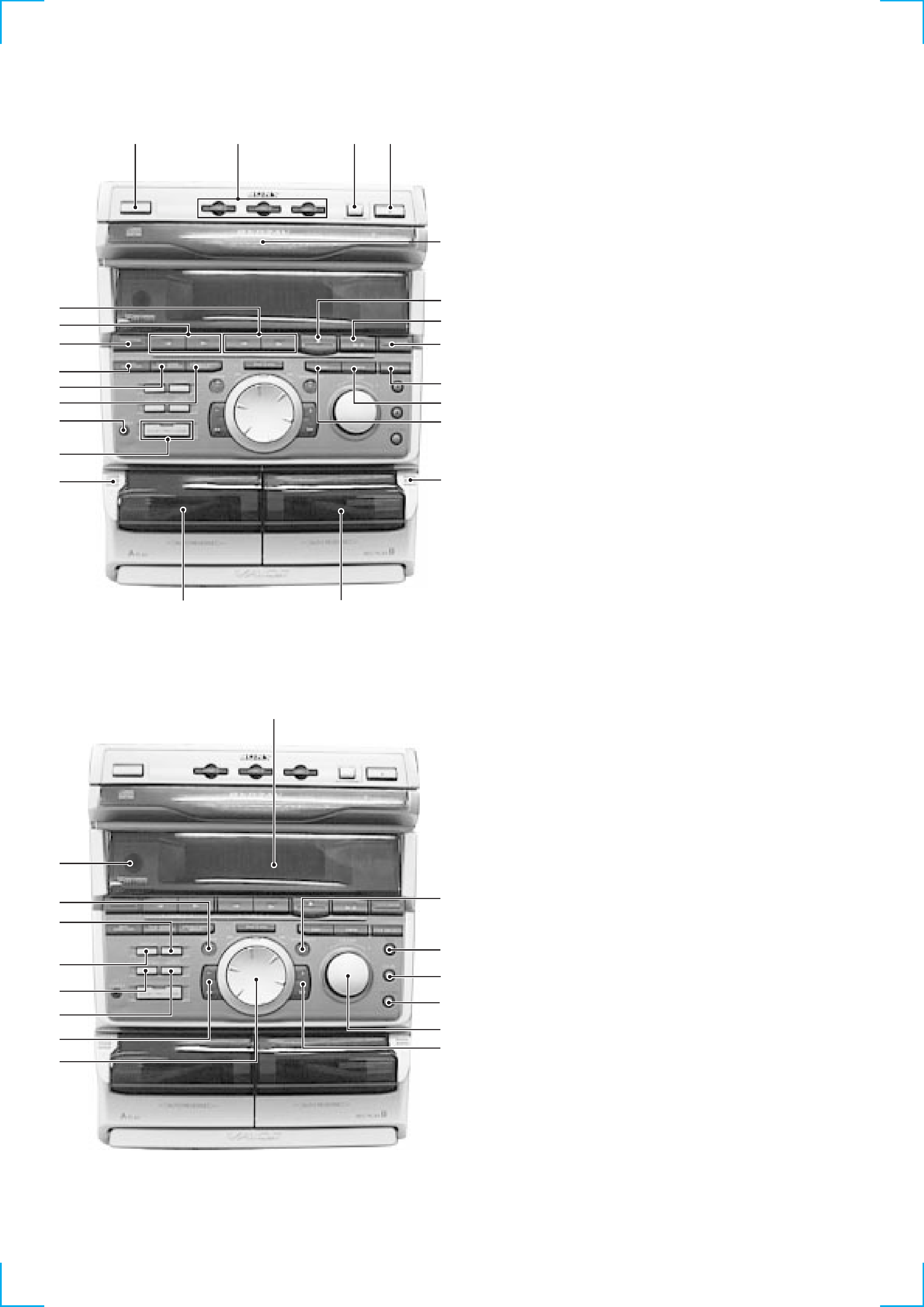
12
3
4
5
6
7
8
9
0
!¡
!TM
!£
!¢
!
!§
!¶
!·
!ª
@º
@¡
@TM
@£
@¢
@
@§
@¶
@·
@ª
#º
#·
#¶
#§
#¢
#
#£
#TM
#¡
@¢
Fluorescent indicator tube
@
ENTER/NEXT button and indicator
@§
REC button and indicator
@¶
PAUSE button and indicator
@·
CD SYNC button
@ª
VOLUME knob
#º
+,
) button and indicator
#¡
JOG dial
#TM
,
0 button and indicator
#£
TIMER SELECT button and indicator
#¢
CLOCK/TIMER SET button
#
DISPLAY button
#§
DEMO button
#¶
GROOVE button and indicator
#·
Remote sensor
1
1/u (Power) button and indicator
2
DISC 1 to 3 button and indicators
3
DISC SKIP button
4
§ (CD) button
5
CD disc tray
6
p button
7
CD,
^ button and indicator
8
TUNER/BAND button
9
FILE SELECT button
0
DBFB button
!¡
DSP button
!TM
§ (deck B)
!£
Tape deck B
!¢
Tape deck A
!
§ (deck A)
!§
DOLBY PRO LOGIC button
!¶
PHONES jack
!·
REPEAT, STEREO/MONO button
!ª
PLAY MODE, TUNER MEMORY button
@º
EDIT DIRECTION button
@¡
FUNCTION button
@TM
TAPE A,
9 and ( buttons and indicators
@£
TAPE B,
9 and ( buttons and indicators
5
This section is extracted
from instruction manual.