SERVICE MANUAL
COMPACT DISC DECK RECEIVER
HCD-NEZ30
Ver. 1.5 2007.04
SPECIFICATIONS
9-887-030-06
2007D05-1
© 2007.04
Sony Corporation
Personal Audio Division
Published by Sony Techno Create Corporation
US Model
Canadian Model
UK Model
E Model
East European Model
· HCD-NEZ30 is the amplifier, CD player, tape deck
and tuner section in CMT-NEZ30.
Model Name Using Similar Mechanism
HCD-NEZ3
CD Section
Base Unit Name
BU-K8BD83S-WOD
Optical Pick-up block Name
KSM-213CDP
TAPE Section
Model Name Using Similar Mechanism
NEW
Tape Transport Mechanism Type
CMAL5Z235A
AUDIO POWER SPECIFICATIONS
POWER OUTPUT AND TOTAL HARMONIC DISTORTION:
(The United States model only)
With 6 ohm loads, both channels driven, from 120 10,000 Hz; rated 15 watts
per channel minimum RMS power, with no more than 10% total harmonic
distortion from 250 milliwatts to rated output.
Amplifier section
North-American model:
Continuous RMS power output (reference): 15 + 15 W (6 ohms at 1 kHz,
10% THD)
European model:
DIN power output (rated): 11 + 11 W (6 ohms at 1 kHz, DIN)
Continuous RMS power output (reference): 17 + 17 W (6 ohms at 1 kHz,
10% THD)
Music power output (reference): 28 + 28 W
The following are measured at AC 220 V, 50/60 Hz (Argentine model), AC
120 V, 60 Hz (Mexican model), AC 120, 220 or 230 240 V, 50/60 Hz (other
models)
DIN power output (rated): 11 + 11 W (6 ohms at 1 kHz, DIN)
Continuous RMS power output (reference): 15 + 15 W (6 ohms at 1 kHz,
10% THD)
Inputs
AUDIO IN: Sensitivity 250 mV, impedance 47 kilohms
Outputs
PHONES: Accepts headphones with an impedance of 8 ohms or more
SPEAKER: Accepts impedance of 6 to 16 ohms
CD player section
System: Compact disc and digital audio system
Laser Diode Properties
Emission Duration: Continuous
Laser Output*: Less than 44.6
µW
* This output is the value measurement at a distance of 200 mm from the
objective lens surface on the Optical Pick-up Block with 7mm aperture.
Tape deck section
Recording system: 4-track 2-channel, stereo
AM tuner section:
Tuning range
Pan-American model: 530 1,710 kHz (with 10 kHz tuning interval)
531 1,710 kHz (with 9 kHz tuning interval)
Other models: 530 1,710 kHz (with 10 kHz tuning interval)
European models: 531 1,602 kHz (with 9 kHz tuning interval)
531 1,602 kHz (with 9 kHz tuning interval)
Antenna: AM loop antenna, external antenna terminal
Intermediate frequency: 450 kHz
General
Power requirements
North American model: AC 120 V, 60 Hz
Mexican model: AC 120 V, 60 Hz
European model: AC 230 V, 50/60 Hz
Argentine model: AC 220 V, 50/60 Hz
Other models: AC 120, 220 or 230 240 V, 50/60 Hz
Adjustable with voltage selector
Power consumption:
North American model: 45 watts
Other models: 45 watts
Dimensions (w/h/d) (excl. speakers):
Mass (excl. speakers):
North
Approx. 164
× 235 × 265 mm
American model: Approx. 3.2 kg
European model: Approx. 3.6 kg
Other models: Approx. 3.3 kg
Design and specifications are subject to change without notice.
Tuner section
FM stereo, FM/AM superheterodyne tuner
FM tuner section:
Tuning range
North American model: 87.5 108.0 MHz (100 kHz step)
Other models: 87.5 108.0 MHz (50 kHz step)
Antenna: FM lead antenna
Antenna terminals: 75 ohms unbalanced
Intermediate frequency: 10.7 MHz
2
HCD-NEZ30
Notes on chip component replacement
· Never reuse a disconnected chip component.
· Notice that the minus side of a tantalum capacitor may be
damaged by heat.
Flexible Circuit Board Repairing
· Keep the temperature of the soldering iron around 270 °C
during repairing.
· Do not touch the soldering iron on the same conductor of the
circuit board (within 3 times).
· Be careful not to apply force on the conductor when soldering
or unsoldering.
CAUTION
Use of controls or adjustments or performance of procedures
other than those specified herein may result in hazardous radiation
exposure.
SAFETY-RELATED COMPONENT WARNING!!
COMPONENTS IDENTIFIED BY MARK 0 OR DOTTED LINE
WITH MARK 0 ON THE SCHEMATIC DIAGRAMS AND IN
THE PARTS LIST ARE CRITICAL TO SAFE OPERATION.
REPLACE THESE COMPONENTS WITH SONY PARTS WHOSE
PART NUMBERS APPEAR AS SHOWN IN THIS MANUAL OR
IN SUPPLEMENTS PUBLISHED BY SONY.
ATTENTION AU COMPOSANT AYANT RAPPORT
À LA SÉCURITÉ!
LES COMPOSANTS IDENTIFIÉS PAR UNE MARQUE 0 SUR
LES DIAGRAMMES SCHÉMATIQUES ET LA LISTE DES
PIÈCES
SONT
CRITIQUES
POUR
LA
SÉCURITÉ
DE
FONCTIONNEMENT. NE REMPLACER CES COM- POSANTS
QUE PAR DES PIÈCES SONY DONT LES NUMÉROS SONT
DONNÉS DANS CE MANUEL OU DANS LES SUPPLÉMENTS
PUBLIÉS PAR SONY.
SAFETY CHECK-OUT
After correcting the original service problem, perform the following
safety check before releasing the set to the customer:
Check the antenna terminals, metal trim, "metallized" knobs, screws,
and all other exposed metal parts for AC leakage.
Check leakage as described below.
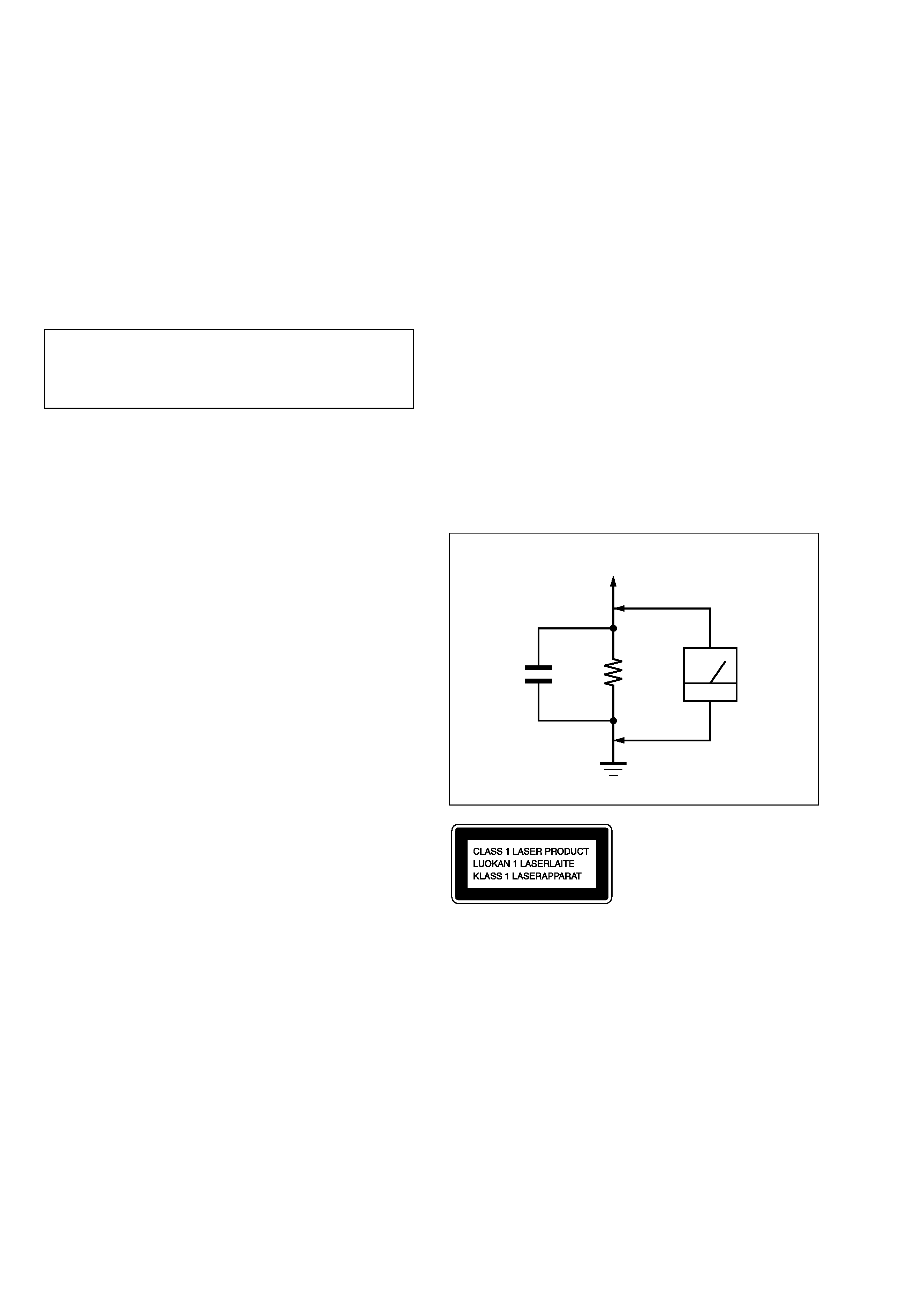
Fig. A.
Using an AC voltmeter to check AC leakage.
1.5 k
0.15
µF
AC
voltmeter
(0.75 V)
To Exposed Metal
Parts on Set
Earth Ground
LEAKAGE TEST
The AC leakage from any exposed metal part to earth ground and
from all exposed metal parts to any exposed metal part having a
return to chassis, must not exceed 0.5 mA (500 microamperes.).
Leakage current can be measured by any one of three methods.
1. A commercial leakage tester, such as the Simpson 229 or RCA
WT-540A. Follow the manufacturers' instructions to use these
instruments.
2. A battery-operated AC milliammeter. The Data Precision 245
digital multimeter is suitable for this job.
3. Measuring the voltage drop across a resistor by means of a
VOM or battery-operated AC voltmeter. The "limit" indication
is 0.75 V, so analog meters must have an accurate low-voltage
scale. The Simpson 250 and Sanwa SH-63Trd are examples
of a passive VOM that is suitable. Nearly all battery operated
digital multimeters that have a 2 V AC range are suitable. (See
Fig. A)
classified as a CLASS
This appliance is
1 LASER product. This
marking is located on the
rear exterior.
3
HCD-NEZ30
SECTION 1
SERVICING NOTES
TABLE OF CONTENTS
1.
SERVICING NOTES ............................................... 3
2.
GENERAL ................................................................... 6
3.
DISASSEMBLY
3-1.
Disassembly Flow ...........................................................
8
3-2.
Cabinet .............................................................................
8
3-3.
Cabinet (Top) Section ......................................................
9
3-4.
Base Unit (BU-K8BD83S-WOD) ...................................
9
3-5.
Front Panel Section ......................................................... 10
3-6.
Mechanical Deck (CMAL5Z235A) ................................ 10
3-7.
MAIN Board .................................................................... 11
3-8.
Tuner (FM/AM) ............................................................... 11
4.
TEST MODE .............................................................. 12
5.
MECHANICAL ADJUSTMENTS ....................... 13
6.
ELECTRICAL ADJUSTMENTS ......................... 14
7.
DIAGRAMS
7-1.
Block Diagram CD SERVO Section ......................... 17
7-2.
Block Diagram MAIN Section .................................. 18
7-3.
Printed Wiring Board CD Board ............................... 20
7-4.
Schematic Diagram CD Board .................................. 21
7-5.
Printed Wiring Boards MAIN Section ...................... 22
7-6.
Schematic Diagram MAIN Section (1/2) .................. 23
7-7.
Schematic Diagram MAIN Section (2/2) .................. 24
7-8.
Printed Wiring Board PANEL Board ........................ 26
7-9.
Schematic Diagram PANEL Board ........................... 27
7-10. Printed Wiring Boards DC Section ........................... 28
7-11. Printed Wiring Board AC Board ................................ 29
7-12. Schematic Diagram POWER SUPPLY Section ........ 30
8.
EXPLODED VIEWS
8-1.
Cabinet Section ................................................................ 36
8-2.
Mechanical Deck Section ................................................ 37
8-3.
Panel Board Section ........................................................ 38
8-4.
Cabinet (Top) Section ...................................................... 39
8-5.
MAIN Board Section ....................................................... 40
8-6.
AC Board, DC Board Section ......................................... 41
9.
ELECTRICAL PARTS LIST ................................ 42
Ver. 1.5
The laser diode in the optical pick-up block may suffer electrostatic
break-down because of the potential difference generated by the
charged electrostatic load, etc. on clothing and the human body.
During repair, pay attention to electrostatic break-down and also
use the procedure in the printed matter which is included in the
repair parts.
The flexible board is easily damaged and should be handled with
care.
NOTES ON HANDLING THE OPTICAL PICK-UP
BLOCK OR BASE UNIT
UNLEADED SOLDER
Boards requiring use of unleaded solder are printed with the lead-
free mark (LF) indicating the solder contains no lead.
(Caution: Some printed circuit boards may not come printed with
the lead free mark due to their particular size)
: LEAD FREE MARK
Unleaded solder has the following characteristics.
· Unleaded solder melts at a temperature about 40 °C higher
than ordinary solder.
Ordinary soldering irons can be used but the iron tip has to be
applied to the solder joint for a slightly longer time.
Soldering irons using a temperature regulator should be set to
about 350 °C.
Caution: The printed pattern (copper foil) may peel away if
the heated tip is applied for too long, so be careful!
· Strong viscosity
Unleaded solder is more viscou-s (sticky, less prone to flow)
than ordinary solder so use caution not to let solder bridges
occur such as on IC pins, etc.
· Usable with ordinary solder
It is best to use only unleaded solder but unleaded solder may
also be added to ordinary solder.
NOTES ON LASER DIODE EMISSION CHECK
The laser beam on this model is concentrated so as to be focused on
the disc reflective surface by the objective lens in the optical pick-
up block. Therefore, when checking the laser diode emission,
observe from more than 30 cm away from the objective lens.
Refer to SUPPLEMENT-1 for the CD board of printed wiring board,
schematic diagram and electrical parts list of UK and East European
models.
When repairing the set of except UK and East European models, refer to
either of original service manual/SUPPLEMENT-1 according to the set.
Refer to SUPPLEMENT-2 for the HEAD PHONE board of printed wiring
board, schematic diagram and electrical parts list of UK and East European
models.
When repairing the set of except UK and East European models, refer to
either of original service manual/SUPPLEMENT-2 according to the set.
Refer to SUPPLEMENT-3 for the PANEL board of printed wiring board,
schematic diagram and electrical parts list of UK and East European
models.
When repairing the set of except UK and East European models, refer to
either of original service manual/SUPPLEMENT-3 according to the set.
Refer to SUPPLEMENT-1 for the MAIN board of printed wiring board,
schematic diagram and electrical parts list of except US and Canadian
models.
When repairing the set of US and Canadian models, refer to either of
original service manual/SUPPLEMENT-1 according to the set.
4
HCD-NEZ30
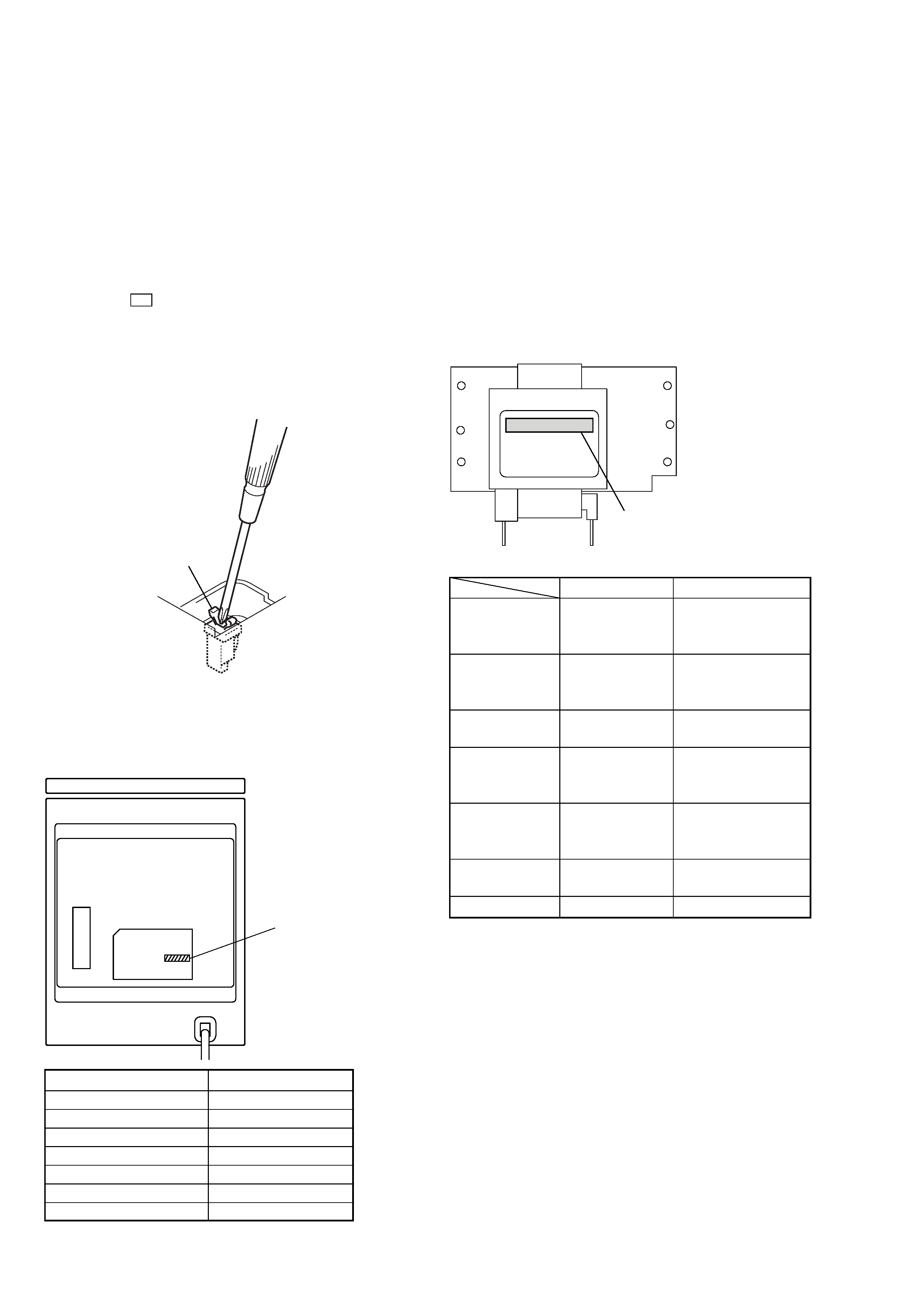
LASER DIODE AND FOCUS SEARCH OPERATION
CHECK
During normal operation of the equipment, emission of the laser
diode is prohibited unless the upper lid is closed while turning ON
the S820. (push switch type)
The following checking method for the laser diode is operable.
· Method
Emission of the laser diode is visually checked.
1. Open the upper lid.
2. Push the S820 as shown in Fig.1.
Note: Do not push the detection lever strongly, or it may be bent or damaged.
3. Press the u button.
4. Check the object lens for confirming normal emission of the
laser diode. If not emitting, there is a trouble in the automatic
power control circuit or the optical pick-up.
In this operation, the object lens will move up and down 2
times along with inward motion for the focus search.
Fig.1 Method to push the S820
S820
Ver. 1.5
MODEL IDENTIFICATION
Rear View
Model Name
Part No.
E model
2-665-907-0[]
Mexican model
2-665-908-0[]
Chilean and Peruvian models
2-665-909-0[]
Argentina model
2-665-910-0[]
US and Canadian models
2-665-913-0[]
UK model
3-100-772-0[]
East European model
3-312-856-0[]
Part No.
NOTE WHEN PARTS RELATED TO POWER
TRANSFORMER ARE REPLACED
In this set, the main power transformer (T902) and sub power
transformer (T901) of US and Canadian models have been changed
in the midway of production.
The mount parts on DC board and Part No. of DC board have been
changed along with it.
Perform after confirming which type set when you repair set because
there is a suited combination.
· DISCRIMINATION
Distinguish by the print of label pasted to side of main power
transformer (T902).
MAIN POWER TRANSFORMER (T902)
· Combination
TYPE A
TYPE B
POWER
1-443-902-11
1-443-903-11
TRANSFORMER
TRANSFORMER,
TRANSFORMER,
(T902)
POWER
POWER
T901
1-443-833-11
1-443-846-11
(on AC board)
TRANSFORMER,
TRANSFORMER,
POWER
POWER
D921
NO MOUNT
6-501-193-01
(on DC board)
DIODE 1SS355WTE-17
R911
1-216-841-11
1-216-829-11
(on DC board)
METAL CHIP
METAL CHIP
47K 5% 1/10W
4.7K 5% 1/10W
R912
1-216-841-11
1-216-845-11
(on DC board)
METAL CHIP
METAL CHIP
47K 5% 1/10W
100K 5% 1/10W
R920
NO MOUNT
1-216-864-11
(on DC board)
SHORT CHIP 0
DC board
A-1158-136-A
A-1216-850-A
1-443-902-11: TYPE A
1-443-903-11: TYPE B
5
HCD-NEZ30
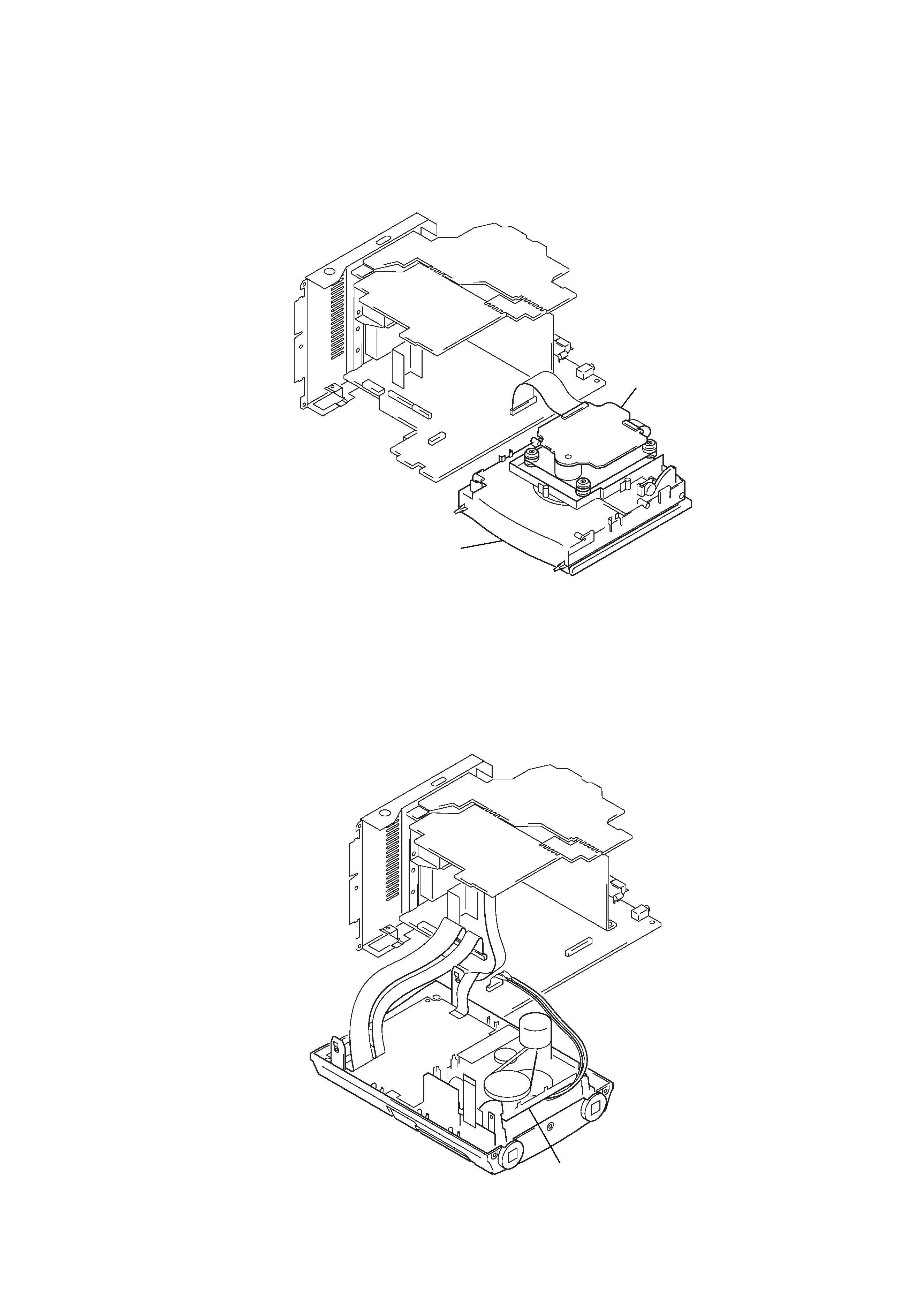
SERVICE POSITION
CD BOARD
TAPE MECHANICAL DECK
CD board
cabinet (top) section
tape mechanical deck