1
HCD-DR7AV/XB800AV
AEP Model
UK Model
HCD-XB800AV
E Model
Australian Model
HCD-DR7AV
SPECIFICATIONS
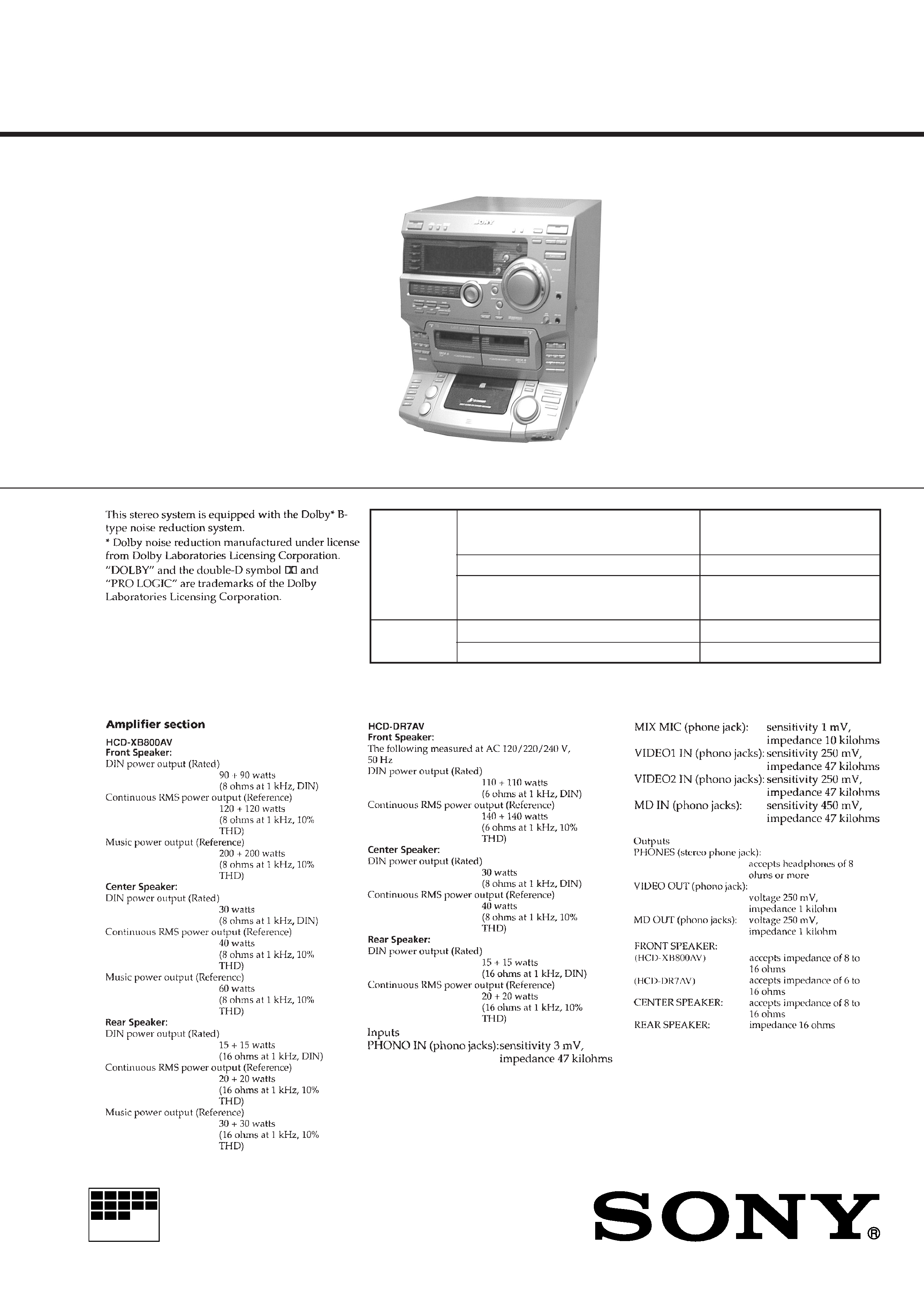
Photo: HCD-DR7AV
COMPACT DISC DECK RECEIVER
-- Continued on next page --
Model Name Using Similar Mechanism
HCD-DR4/DR5/DR6/DR440/
W300/W5000/XB500
CD Mechanism Type
CDM37M-5BD32L
Base Unit Type
BU-5BD32L
Optical Pick-up Type
KSS-213D/Q-N
Model Name Using Similar Mechanism
NEW
Tape Transport Mechanism Type
TCM-230AWR2/230PWR2
CD
SECTION
TAPE DECK
SECTION
HCD-DR7AV/XB800AV is the tuner,
deck, CD and amplifier section in
LBT-DR7AV/XB800AV.
SERVICE MANUAL
MICROFILM
2
3
CAUTION
Use of controls or adjustments or performance of procedures
other than those specified herein may result in hazardous ra-
diation exposure.
Notes on chip component replacement
· Never reuse a disconnected chip component.
· Notice that the minus side of a tantalum capacitor may be
damaged by heat.
Flexible Circuit Board Repairing
· Keep the temperature of soldering iron around 270°C
during repairing.
· Do not touch the soldering iron on the same conductor of the
circuit board (within 3 times).
· Be careful not to apply force on the conductor when soldering
or unsoldering.
SAFETY-RELATED COMPONENT WARNING !!
COMPONENTS IDENTIFIED BY MARK
! OR DOTTED LINE
WITH MARK
! ON THE SCHEMATIC DIAGRAMS AND IN
THE PARTS LIST ARE CRITICAL TO SAFE OPERATION.
REPLACE THESE COMPONENTS WITH SONY PARTS
WHOSE PART NUMBERS APPEAR AS SHOWN IN THIS
MANUAL OR IN SUPPLEMENTS PUBLISHED BY SONY.
Laser component in this product is capable of emitting radiation
exceeding the limit for Class 1.
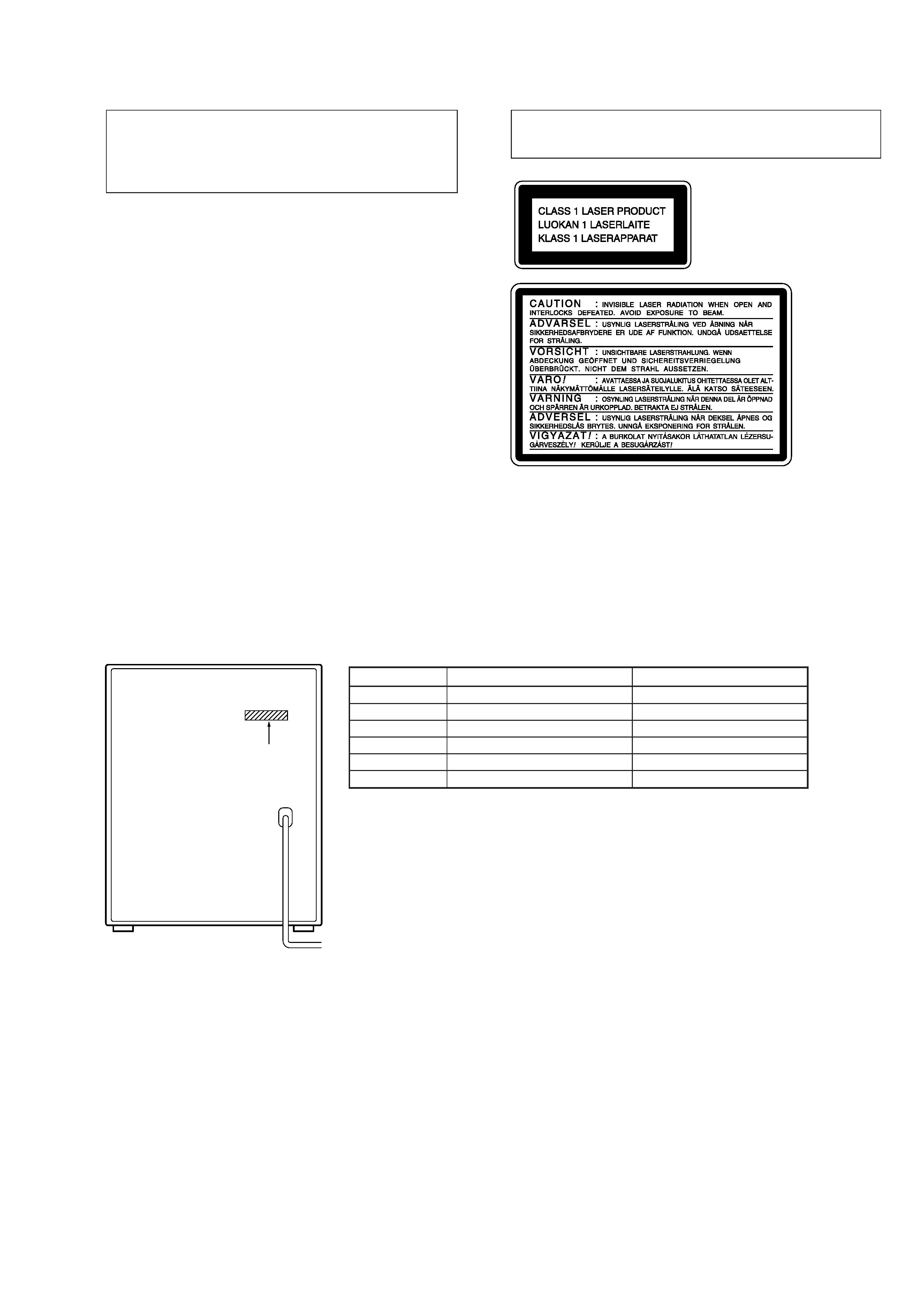
This appliance is classified as
a CLASS 1 LASER product.
The CLASS 1 LASER PROD-
UCT MARKING is located on
the rear exterior.
This caution
label is located
inside the unit.
PARTS No.
MODEL
PRODUCT COUNTRY
4-214-788-0
DR7AV: SP
INDONESIA
4-214-788-1
DR7AV: EA
INDONESIA
4-214-788-2
DR7AV: AUS
INDONESIA
4-214-788-6
DR7AV: TH
THAILAND
4-214-785-3
XB800AV: AEP, UK, EE, CIS
INDONESIA
4-214-785-4
XB800AV: AEP
THAILAND
MODEL IDENTIFICATION
-- BACK PANEL --
· Abbreviation
SP
: Singapore model
EA
: Saudi Arabia model
AUS : Australian model
TH
: Thailand model
EE
: East European model
Parts No.

4
NOTES ON HANDLING THE OPTICAL PICK-UP BLOCK
OR BASE UNIT
The laser diode in the optical pick-up block may suffer electrostatic
break-down because of the potential difference generated by the
charged electrostatic load, etc. on clothing and the human body.
During repair, pay attention to electrostatic break-down and also
use the procedure in the printed matter which is included in the
repair parts.
The flexible board is easily damaged and should be handled with
care.
NOTES ON LASER DIODE EMISSION CHECK
The laser beam on this model is concentrated so as to be focused on
the disc reflective surface by the objective lens in the optical pick-
up block. Therefore, when checking the laser diode emission, ob-
serve from more than 30 cm away from the objective lens.
LASER DIODE AND FOCUS SEARCH OPERATION
CHECK
Carry out the "S curve check" in "CD section adjustment" and check
that the S curve waveform is output four times.
SECTION 1
SERVICING NOTE
About CD-TEXT display
This unit is provided with a simple CD-TEXT display function.
The CD-TEXT contents of 20 tracks are displayed on the fluores-
cent display tube.
Since the function is simple, some special characters may not be
displayed, or may be displayed as other characters.

5
TABLE OF CONTENTS
7-15. Printed Wiring Board Power Section
(DR7AV model) ................................................................ 61
7-16. Schematic Diagram Power (1/2) Section
(XB800AV model) ............................................................ 63
7-17. Schematic Diagram Power (2/2) Section
(XB800AV model) ............................................................ 65
7-18. Printed Wiring Board Power Section
(XB800AV model) ............................................................ 67
7-19. Schematic Diagram Panel FL Section ........................ 69
7-20. Printed Wiring Board Panel FL Section ..................... 71
7-21. Schematic Diagram Panel VR Section ....................... 73
7-22. Printed Wiring Board Panel VR Section .................... 75
7-23. Schematic Diagram TC Panel Section ....................... 77
7-24. Printed Wiring Board TC Panel Section ..................... 79
7-25. Schematic Diagram CD Panel Section ....................... 81
7-26. Printed Wiring Board CD Panel Section .................... 83
7-27. Schematic Diagram CD Motor Section ...................... 85
7-28. Printed Wiring Board CD Motor Section ................... 87
7-29. Schematic Diagram Jack Section ............................... 89
7-30. Printed Wiring Board Jack Section ............................ 91
7-31. Schematic Diagram Trans Section
(XB800AV model) ............................................................ 93
7-32. Printed Wiring Board Trans Section
(XB800AV model) ............................................................ 95
7-33. Schematic Diagram Trans Section
(DR7AV model) ................................................................ 97
7-34. Printed Wiring Board Trans Section
(DR7AV model) ................................................................ 99
7-35. Schematic Diagram Leaf SW Section ...................... 100
7-36. Printed Wiring Board Leaf SW Section ................... 100
7-37. Schematic Diagram Surround Section ..................... 101
7-38. Printed Wiring Board Surround Section ................... 101
7-39. IC Block Diagrams ......................................................... 103
7-40. IC Pin Functions ............................................................. 104
8. EXPLODED VIEWS
8-1. Case and Back Panel Section ............................................ 107
8-2. Front Panel Section 1 ........................................................ 108
8-3. Front Panel Section 2 ........................................................ 109
8-4. Chassis Section ................................................................. 110
8-5. TC Mechanism Section 1 (TCM230AWR2/230PWR2) ... 111
8-6. TC Mechanism Section 2 (TCM230AWR2/230PWR2) ... 112
8-7. CD Mechanism Section (CDM37M-5BD32L) ................. 113
8-8. Base Unit Section (BU-5BD32L) ..................................... 114
9. ELECTRICAL PARTS LIST ...................................... 115
1. SERVICING NOTE .......................................................... 4
2. GENERAL .................................................................... 6
3. DISASSEMBLY
3-1. Front Panel ............................................................................ 8
3-2. Main Board ........................................................................... 8
3-3. Sub Panel .............................................................................. 9
3-4. CD-L/CD-R Board and CD Lid Assembly ........................... 9
3-5. Tape Mechanism Deck and Cassette Lid ............................ 10
3-6. CD Mechanism Deck .......................................................... 10
3-7. Base Unit ............................................................................. 10
3-8. Disc Table ........................................................................... 11
4. SERVICE MODE ............................................................ 12
5. MECHANICAL ADJUSTMENTS .......................... 16
6. ELECTRICAL ADJUSTMENTS ............................... 16
7. DIAGRAMS
7-1. Circuit Boards Location ...................................................... 19
7-2. Block Diagrams
· BD (CD) Section .............................................................. 21
· Deck Section .................................................................... 23
· Main (1/2) Section ........................................................... 25
· Main (2/2) Section ........................................................... 27
· Power Section (DR7AV model) ....................................... 29
· Power Section (XB800AV model) ................................... 31
· Display Section ................................................................ 33
7-3. Printed Wiring Board BD (CD) Section ....................... 37
7-4. Schematic Diagram BD (CD) Section .......................... 39
7-5. Printed Wiring Board Main Section .............................. 41
7-6. Schematic Diagram Main (1/5) Section ........................ 43
7-7. Schematic Diagram Main (2/5) Section ........................ 45
7-8. Schematic Diagram Main (3/5) Section ........................ 47
7-9. Schematic Diagram Main (4/5) Section ........................ 49
7-10. Schematic Diagram Main (5/5) Section ..................... 51
7-11. Schematic Diagram Deck Section .............................. 53
7-12. Printed Wiring Board Deck Section ........................... 55
7-13. Schematic Diagram Power (1/2) Section
(DR7AV model) ................................................................ 57
7-14. Schematic Diagram Power (2/2) Section
(DR7AV model) ................................................................ 59