SERVICE MANUAL
MICRO HiFi COMPONENT SYSTEM
SPECIFICATIONS
HCD-CP2
Dolby noise reduction manufactured under license
from Dolby Laboratories Licensing Corporation.
"DOLBY" and the double-D symbol ; are trade-
marks of Dolby Laboratories Licensing Corporation.
AEP Model
UK Model
E Model
Australian Model
HCD-CP2 is the Amplifier, CD player,
Tape Deck and Tuner section in
CMT-CP2.
Continued on next page
Model Name Using Similar Mechanism
NEW
CD Mechanism Type
KSL-2130CCP/K1N
Optical Pick-up Name
KSS-213C/K1N
Model Name Using Similar Mechanism
HCD-W550
Tape Transport Mechanism Type
TCM-220WR2E
CD
Section
Tape deck
Section
2
SAFETY-RELATED COMPONENT WARNING!!
COMPONENTS IDENTIFIED BY MARK 0 OR DOTTED
LINE WITH MARK 0 ON THE SCHEMATIC DIAGRAMS
AND IN THE PARTS LIST ARE CRITICAL TO SAFE
OPERATION. REPLACE THESE COMPONENTS WITH
SONY PARTS WHOSE PART NUMBERS APPEAR AS
SHOWN IN THIS MANUAL OR IN SUPPLEMENTS PUB-
LISHED BY SONY.
TABLE OF CONTENTS
1.
SERVICING NOTES ............................................... 3
2.
GENERAL
Location of Controls .......................................................
4
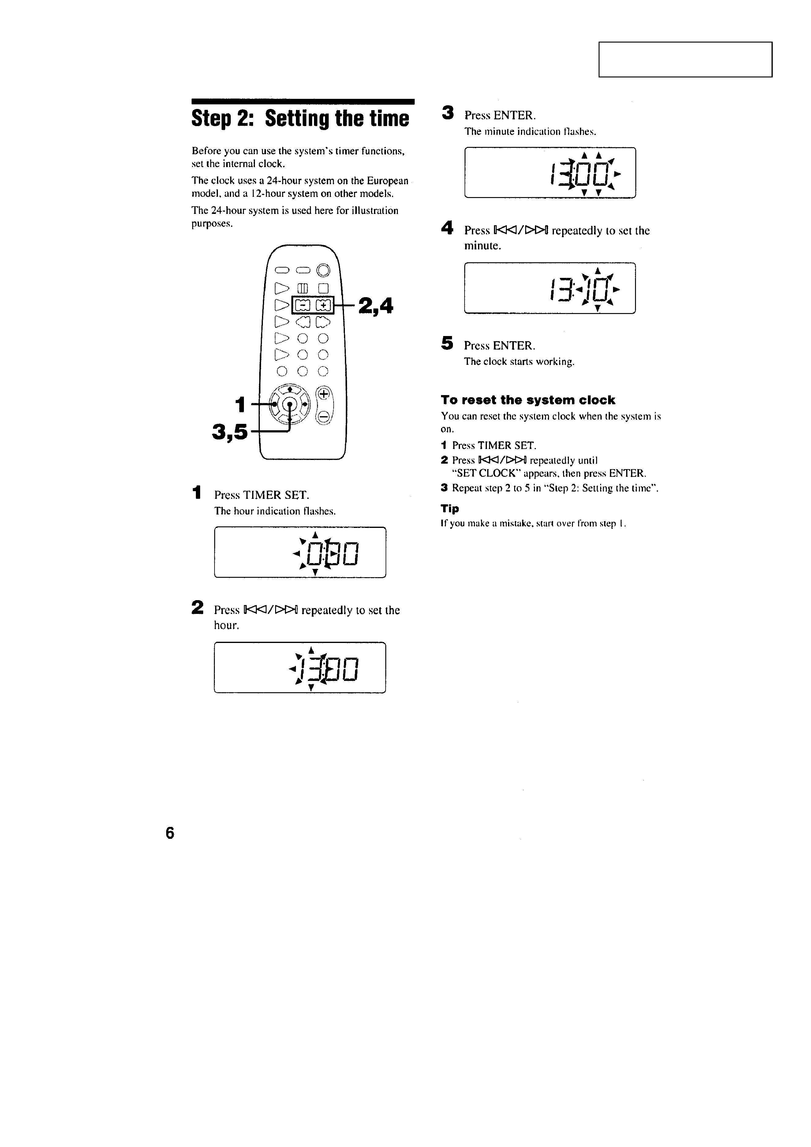
Setting the Time ..............................................................
5
3.
DISASSEMBLY ......................................................... 6
4.
TEST MODE .............................................................. 11
5.
MECHANICAL ADJUSTMENTS ....................... 14
6.
ELECTRICAL ADJUSTMENTS ......................... 14
7.
DIAGRAMS
7-1. Block Diagram CD Section ...................................... 19
7-2. Block Diagram TAPE DECK Section ...................... 20
7-3. Block Diagram MAIN Section ................................. 21
7-4. Block Diagram
DISPLAY/POWER SUPPLY Section ...................... 22
7-5. Note for Printed Wiring Boards and
Schematic Diagrams ....................................................... 23
7-6. Printed Wiring Board CD Section ............................ 24
7-7. Schematic Diagram CD Section ............................... 25
7-8. Printed Wiring Boards TAPE DECK Section .......... 26
7-9. Schematic Diagram TAPE DECK Section ............... 27
7-10. Printed Wiring Board MAIN Board ......................... 28
7-11. Printed Wiring Boards LCD/LOADING Boards ..... 29
7-12. Schematic Diagram MAIN Section (1/3) ................. 31
7-13. Schematic Diagram MAIN Section (2/3) ................. 32
7-14. Schematic Diagram MAIN Section (3/3) ................. 33
7-15. Printed Wiring Boards
AMP/HEADPHONE Boards .................................... 34
7-16. Schematic Diagram POWER AMP Section ............. 35
7-17. Printed Wiring Board CONTROL Board ................. 36
7-18. Schematic Diagram KEY CONTROL Section ........ 37
7-19. Printed Wiring Board POWER Board ...................... 38
7-20. Schematic Diagram POWER SUPPLY Section ....... 38
7-21. IC Pin Function Description ........................................... 44
8.
EXPLODED VIEWS ................................................ 47
9.
ELECTRICAL PARTS LIST ............................... 54
3
SECTION 1
SERVICING NOTES
The laser diode in the optical pick-up block may suffer electro-
static break-down because of the potential difference generated
by the charged electrostatic load, etc. on clothing and the human
body.
During repair, pay attention to electrostatic break-down and also
use the procedure in the printed matter which is included in the
repair parts.
The flexible board is easily damaged and should be handled with
care.
NOTES ON LASER DIODE EMISSION CHECK
The laser beam on this model is concentrated so as to be focused
on the disc reflective surface by the objective lens in the optical
pick-up block. Therefore, when checking the laser diode emis-
sion, observe from more than 30 cm away from the objective lens.
Notes on chip component replacement
· Never reuse a disconnected chip component.
· Notice that the minus side of a tantalum capacitor may be dam-
aged by heat.
Flexible Circuit Board Repairing
· Keep the temperature of the soldering iron around 270 °C dur-
ing repairing.
· Do not touch the soldering iron on the same conductor of the
circuit board (within 3 times).
· Be careful not to apply force on the conductor when soldering
or unsoldering.
NOTES ON HANDLING THE OPTICAL PICK-UP
BLOCK OR BASE UNIT
CAUTION
Use of controls or adjustments or performance of procedures
other than those specified herein may result in hazardous ra-
diation exposure.
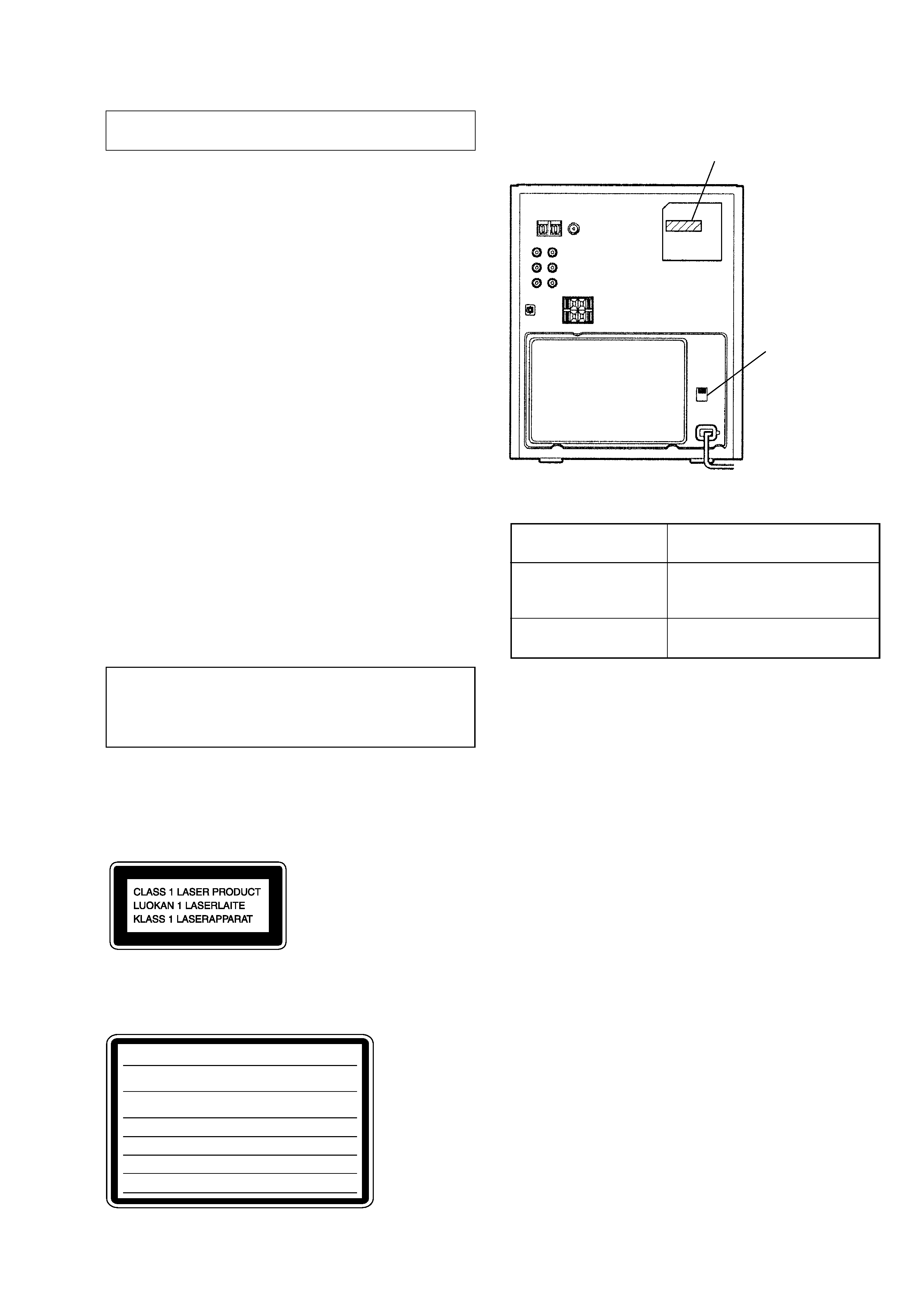
This appliance is classified as a CLASS 1 LASER product.
The CLASS 1 LASER PRODUCT MARKING is located on
the rear exterior.
Laser component in this product is capable of emitting radiation
exceeding the limit for Class 1.
The following caution label is located inside the unit.
CAUTION
: INVISIBLE LASER RADIATION WHEN OPEN AND
INTERLOCKS DEFEATED.
AVOID EXPOSURE TO BEAM.
ADVARSEL : USYNLIG LASERSTRÅLING VED ÅBNING NÅR
SIKKERHEDSAFBRYDERE ER UDE AF FUNKTION. UNDGÅ UDSAETTELSE
FOR STRÅLING.
VORSICHT : UNSICHTBARE LASERSTRAHLUNG, WENN
ABDECKUNG GEÖFFNET UND SICHEREITSVERRIEGELUNG
ÜBERBRÜCKT. NICHT DEM STRAHL AUSSETZEN.
VARO!
: AVATTAESSA JA SUOJALUKITUS OHITETTAESSA OLET ALT-
TIINA NÄKYMÄTTÖMÄLLE LASERSÄTEILYLLE. ÄLÄ KATSO SÄTEESEEN.
VARNING
: OSYNLING LASERSTRÅLING NÄR DENNA DEL ÄR ÖPPNAD
OCH SPÄRREN ÄR URKOPPLAD. BETRAKTA EJ STRÅLEN.
ADVERSEL : USYNLIG LASERSTRÅLING NÅR DEKSEL ÅPNES OG
SIKKERHEDSLÅS BRYTES. UNNGÅ EKSPONERING FOR STRÅLEN.
VIGYAZAT! : A BURKOLAT NYITÁSAKOR LÁTHATATLAN LÉZERSU-
GÁRVESZÉLY! KERÜLJE A BESUGÁRZÁST!
· MODEL IDENTIFICATION
Rear Panel
Model
Power Voltage Indication
AEP, UK and
North European and
AC: 230 V -50 Hz 70 W
Australian models
Saudi Arabia,
AC: 110 120/
Singapore models
220 240 V -50/60 Hz 70 W
Power Voltage Indication
VOLTAGE SELECTOR
Switch
4
SECTION 2
GENERAL
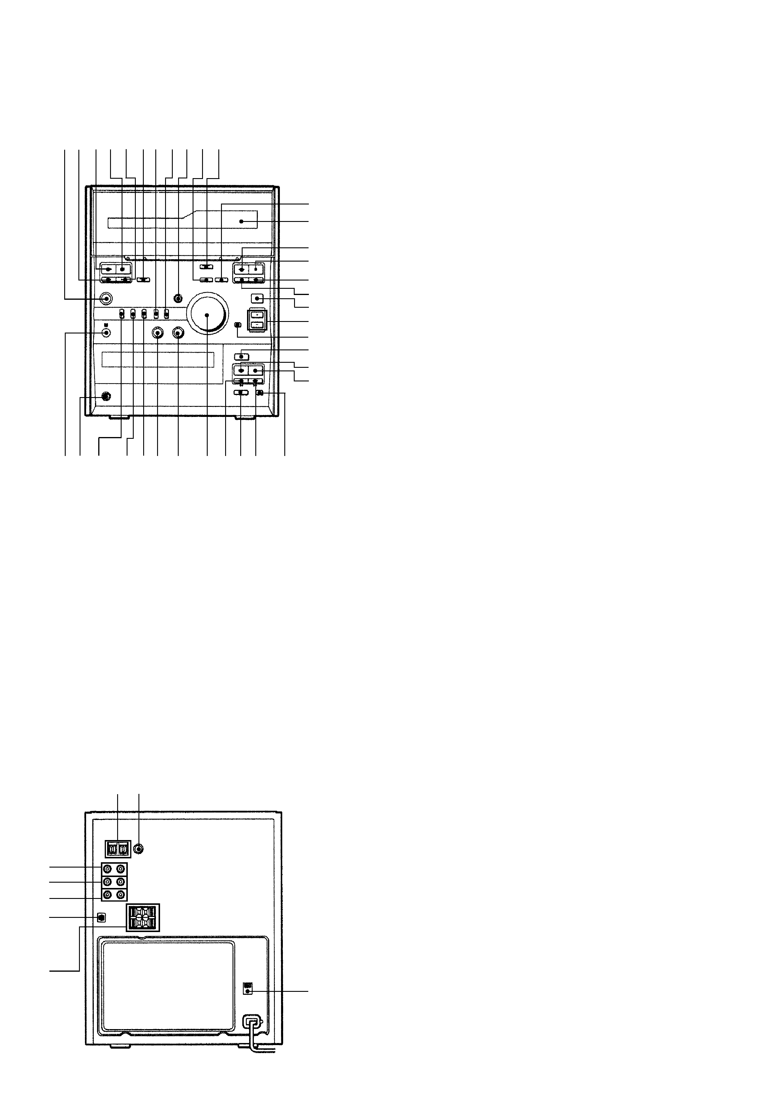
· LOCATION OF CONTROLS
Front View
1 STANDBY ?/1 button and indicator
2 TAPE A m button
3 TAPE A Y button
4 TAPE A x button
5 TAPE A M button
6 HI-SPEED DUBBING button and indicator
7 CD button and indicator
8 TUNER button and indicator
9 DSG button and indicator
0 X button
qa CD SYNC button and indicator
qs REC z button
qd Liquid crystal display
qf TAPE B Y button
qg TAPE B x button
qh TAPE B M button
qj TAPE B m button
qk TUNER BAND button
ql TUNING +/ buttons
w; TUNING MODE button
wa EJECT Z button
ws CD u button
wd CD x button
wf Remote sensor
wg PHONES jack
wh VIDEO button and indicator
wj MD button and indicator
wk TAPE button and indicator
wl BASS switch
e; TREBLE switch
ea VOLUME knob
es CD . m button
ed PLAY MODE button
ef CD > M button
eg REPEAT button
1 AM ANTENNA terminals
2 FM ANTENNA jack or terminals
3 VOLTAGE SELECTOR switch
(Saudi Arabia, singapore models)
4 LINE OUT jacks
5 MD IN jacks
6 VIDEO IN jacks
7 DIGITAL OUT OPTICAL (CD) connector
8 SPEAKER terminals
2
1
3
4
5
6
7
8
Rear View
3
wd
4 5
2
1
7
6
ql
w;
wa
ws
qk
qj
qh
qg
qf
qd
qs
qa
0
9
8
eg
ef
ed
es
wj wk
ea
e;
wl
wh
wg
wf
5
This section is extracted from
instruction manual.