HCD-CL1/CL3
US Model
Australian Model
HCD-CL1
AEP Model
UK Model
E Model
HCD-CL1/CL3
SERVICE MANUAL
COMPACT HiFi COMPONENT SYSTEM
Sony Corporation
Audio Entertainment Group
General Engineering Dept.
9-873-852-11
2001C1600-1
© 2001.3
-- Continued on next page --
SPECIFICATIONS
Ver 1.0 2001. 03
This set is the tuner, deck, CD and amplifier
section in CHC-CL1/CL3.
Model Name Using Similar Mechanism
HCD-DX50
CD Mechanism Type
CDM63B
Base Unit Type
BU-30BD60
Optical Pick-up Type
A-MAX.3
Model Name Using Similar Mechanism
HCD-CL5MD
Tape Transport Mechanism Type
TCM-230ASR41CL
CD
SECTION
TAPE DECK
SECTION
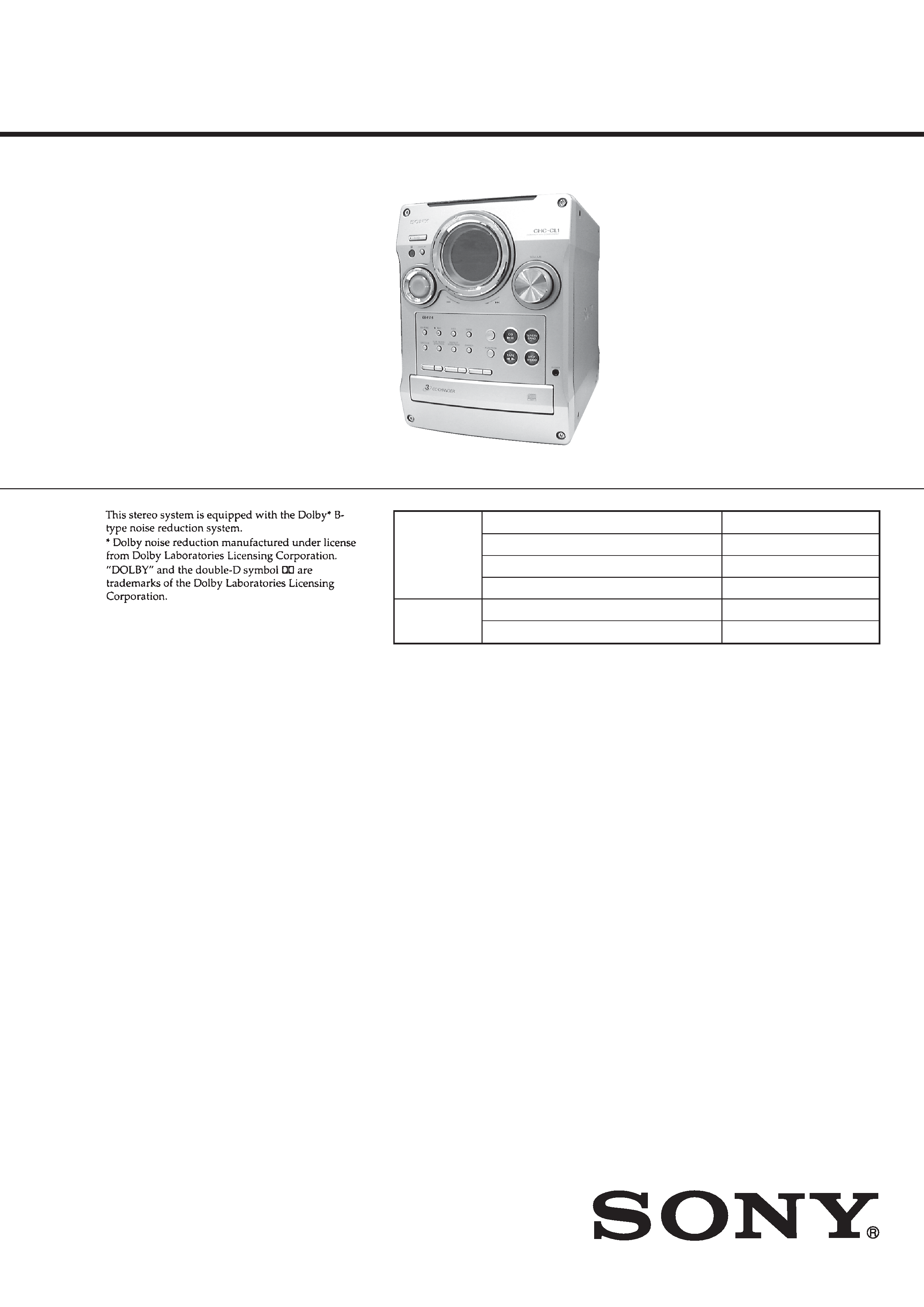
Photo : HCD-CL1
Amplifier section
For the U.S. model
AUDIO POWER SPECIFICATIONS
POWER OUTPUT AND TOTAL HARMONIC
DISTORTION:
With 6-ohm loads, both channels driven, from 120
10,000 Hz; rated 50 watts per channel minimum RMS
power, with no more than 10% total harmonic
distortion from 250 milli watts to rated output.
Total harmonic distortion: less than 0.1% (6 ohms at
1 kHz, 25 W)
AEP models
HCD-CL3:
DIN power output (Rated): 80 + 80 watts
(6 ohms at 1 kHz, DIN)
Continuous RMS power output (Reference):
100 + 100 watts
(6 ohms at 1 kHz, 10%
THD)
Music power output (Reference):
180 + 180 watts
(6 ohms at 1 kHz, 10%
THD)
HCD-CL1:
DIN power output (Rated): 40 + 40 watts
(6 ohms at 1 kHz, DIN)
Continuous RMS power output (Reference):
50 + 50 watts
(6 ohms at 1 kHz, 10%
THD)
Music power output (Reference):
95 + 95 watts
(6 ohms at 1 kHz, 10%
THD)
Other models
The following measured at AC 120/220/240 V, 50/
60 Hz
HCD-CL3:
DIN power output (Rated): 80 + 80 watts
(6 ohms at 1 kHz, DIN)
Continuous RMS power output (Reference):
100 + 100 watts
(6 ohms at 1 kHz, 10%
THD)
HCD-CL1:
DIN power output (Rated): 40 + 40 watts
(6 ohms at 1 kHz, DIN)
Continuous RMS power output (Reference):
50 + 50 watts
(6 ohms at 1 kHz, 10%
THD)
Inputs
MD IN (phono jacks):
voltage 450 mV,
impedance 47 kilohms
Outputs
CD DIGITAL OUT (Supported sampling
frequencies: 32 kHz, 44.1 kHz and 48 kHz)
PHONES (stereo minijack):
accepts headphones of
8 ohms or more.
2
HCD-CL1/CL3
After correcting the original service problem, perform the
following safety checks before releasing the set to the customer:
Check the antenna terminals, metal trim, "metallized" knobs, screws,
and all other exposed metal parts for AC leakage. Check leakage as
described below.
LEAKAGE
The AC leakage from any exposed metal part to earth ground
and from all exposed metal parts to any exposed metal part having
a return to chassis, must not exceed 0.5 mA (500 microamperes).
Leakage current can be measured by any one of three methods.
1.
A commercial leakage tester, such as the Simpson 229 or RCA
WT-540A. Follow the manufacturers' instructions to use these
instruments.
2.
A battery-operated AC milliammeter. The Data Precision 245
digital multimeter is suitable for this job.
3.
Measuring the voltage drop across a resistor by means of a
VOM or battery-operated AC voltmeter. The "limit" indication
is 0.75 V, so analog meters must have an accurate low-voltage
scale. The Simpson 250 and Sanwa SH-63Trd are examples of
a passive VOM that is suitable. Nearly all battery operated
digital multimeters that have a 2V AC range are suitable. (See
Fig. A)
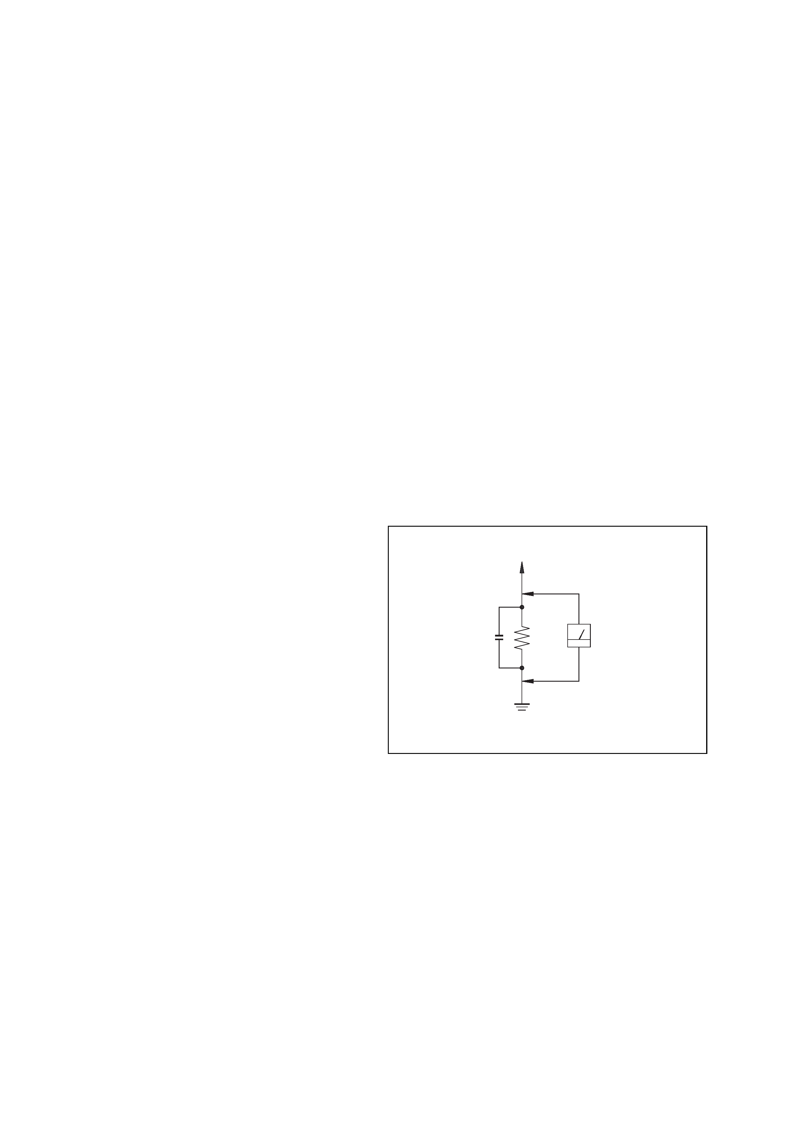
SAFETY CHECK-OUT
To Exposed Metal
Parts on Set
0.15
µF
1.5 k
AC
Voltmeter
(0.75 V)
Earth Ground
Fig. A. Using an AC voltmeter to check AC leakage.
CD player section
System
Compact disc and digital
audio system
Laser
Semiconductor laser
(
=780 nm)
Emission duration:
continuous
Frequency response
2 Hz 20 kHz (
±0.5 dB)
Tape deck section
Recording system
4-track 2-channel stereo
Frequency response
40 13,000 Hz (
±3 dB),
using Sony TYPE I
cassettes
Tuner section
FM stereo, FM/AM superheterodyne tuner
FM tuner section
Tuning range
87.5 108.0 MHz
(50 kHz step)
Antenna
FM lead antenna
Antenna terminals
75 ohms unbalanced
Intermediate frequency
10.7 MHz
AM tuner section
Tuning range
AEP models:
531 1,602 kHz
(with the interval set at
9 kHz)
Other models:
531 1,602 kHz
(with the interval set at
9 kHz)
530 1,710 kHz
(with the interval set at
10 kHz)
Antenna
AM loop antenna
External antenna terminals
Intermediate frequency
450 kHz
General
Power requirements
North American model:
120 V AC, 60 Hz
AEP models:
230 V AC, 50/60 Hz
Australian and New Zealand models:
230 240 V AC, 50/
60 Hz
Mexican model:
120 V AC, 60 Hz
Korean model:
220 V AC, 60 Hz
Other models:
120 V, 220 V, 230
240 V AC, 50/60 Hz
Adjustable with voltage
selector
Power consumption
U.S.A. model:
HCD-CL1:
100 watts
AEP models:
HCD-CL3:
165 watts
HCD-CL1:
100 watts
HCD-CL3/CL1:
0.5 watts (at the Power
Saving Mode)
Other models:
HCD-CL3:
165 watts
HCD-CL1:
100 watts
Dimensions (w/h/d) incl. projecting parts and controls
Approx. 215
× 285 ×
421 mm
Mass
Amplifier/Tuner/Tape/CD section:
HCD-CL3:
Approx. 8.0 kg
HCD-CL1:
Approx. 7.7 kg
Design and specifications are subject to change
without notice.

3
HCD-CL1/CL3
TABLE OF CONTENTS
1. SERVICING NOTES ······················································· 4
2. GENERAL ·········································································· 5
3. DISASSEMBLY
3-1. Top Panel, Side Panel ···················································· 7
3-2. Cassette Mechanism ······················································ 8
3-3. Front Panel ···································································· 8
3-4. Panel Board ··································································· 9
3-5. Back Panel, Main Board ················································ 9
3-6. Amp Board, Power Transformer ································· 10
3-7. CD Mechanism ···························································· 10
3-8. CD Base Unit (BU-30BD60) ······································ 11
3-9. Driver Board ································································ 12
3-10. Fitting Base (Stabilizer) Assy, Tray Assy, ··················· 12
3-11. Tray Sensor Board ······················································· 13
3-12. Slider (Loading), Gear (Slider) ··································· 13
3-13. Stocker Assy, Tray (Sub) ············································· 14
3-14. Disc Sensor Board ······················································· 14
3-15. IN OUT SW Board ······················································ 15
3-16. Motor Assy (M721), Motor Board ······························ 15
4. TEST MODE ···································································· 16
5. MECHANICAL ADJUSTMENTS ····························· 17
6. ELECTRICAL ADJUSTMENTS ······························· 17
7. DIAGRAMS
7-1. Circuit Boards Location ·············································· 21
7-2. Block Diagrams CD Section ······································· 22
Syscon Section ···························································· 23
Main Section ······························································· 24
7-3. Printed Wiring Board Main Section ··························· 25
7-4. Schematic Diagram Main Section (1/2) ····················· 26
7-5. Schematic Diagram Main Section (2/2) ····················· 27
7-6. Schematic Diagram BD Section ································· 28
7-7. Printed Wiring Board BD Section ······························ 29
7-8. Schematic Diagram Driver Section ···························· 30
7-9. Printed Wiring Board Driver Section ························· 31
7-10. Schematic Diagram TC Section ································· 32
7-11. Printed Wiring Board TC Section ······························· 33
7-12. Schematic Diagram AMP Section ······························ 34
7-13. Printed Wiring Board AMP Section ··························· 35
7-14. Schematic Diagram Panel Section ····························· 36
7-15. Printed Wiring Board Panel Section ··························· 37
7-16. Schematic Diagram Trans Section ····························· 38
7-17. Printed Wiring Board Trans Section ··························· 39
7-18. Schematic Diagram Power Section ···························· 40
7-19. Printed Wiring Board Power Section ························· 41
7-20. IC Pin Function Description ········································ 42
7-21. IC Block Diagrams ······················································ 44
8. EXPLODED VIEWS
8-1. Side Panel, Back Panel Section ··································· 46
8-2. Front Panel Section ····················································· 48
8-3. Chassis Section ···························································· 49
8-4. CD Mechanism Deck Section-1 ·································· 50
8-5. CD Mechanism Deck Section-2 ·································· 51
8-6. Base Unit Section (BU-30BD60) ································ 52
9. ELECTRICAL PARTS LIST ······································· 53
4
HCD-CL1/CL3
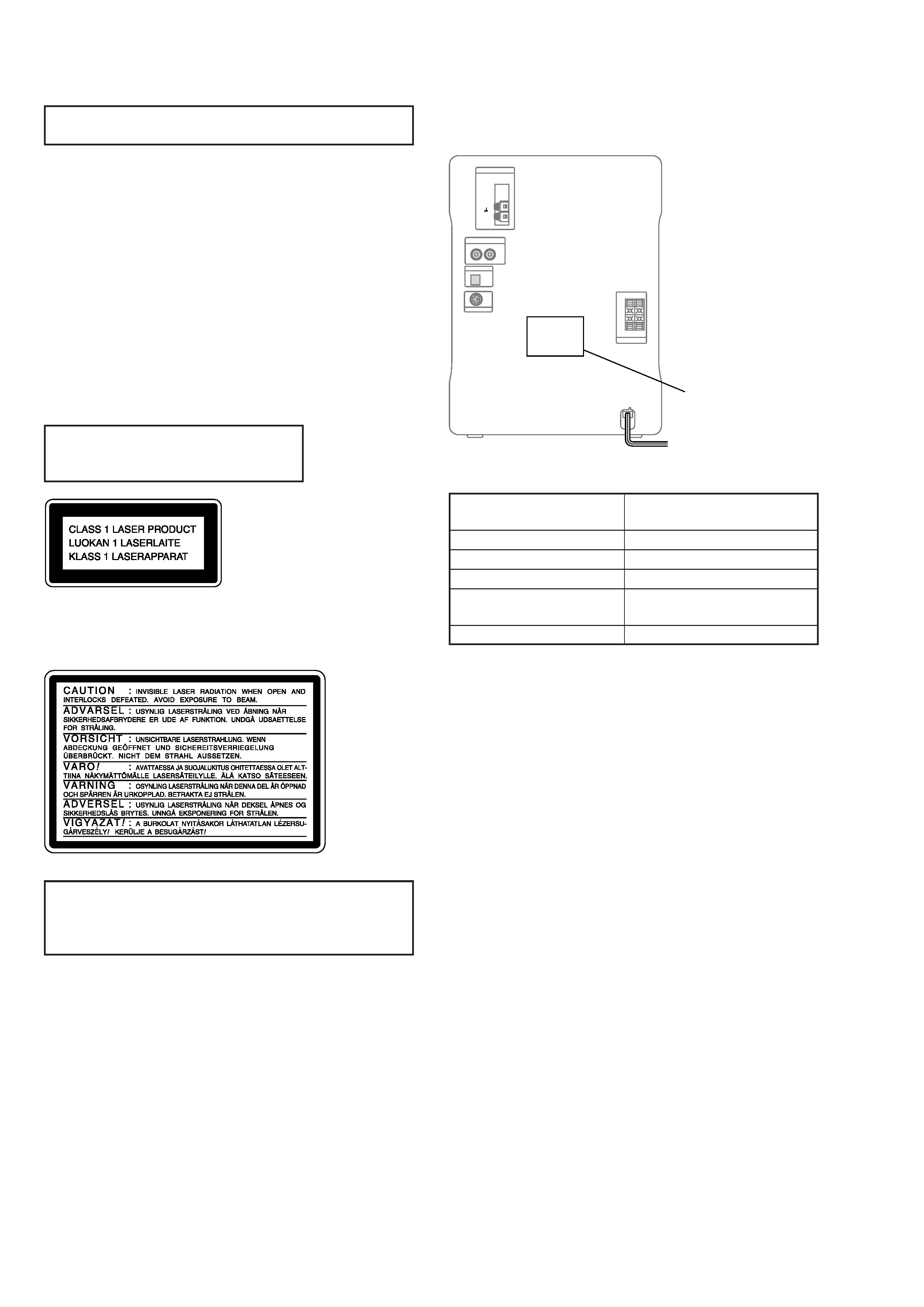
SAFETY-RELATED COMPONENT WARNING!!
COMPONENTS IDENTIFIED BY MARK 0 OR DOTTED LINE WITH
MARK 0 ON THE SCHEMATIC DIAGRAMS AND IN THE PARTS
LIST ARE CRITICAL TO SAFE OPERATION. REPLACE THESE
COMPONENTS WITH SONY PARTS WHOSE PART NUMBERS
APPEAR AS SHOWN IN THIS MANUAL OR IN SUPPLEMENTS
PUBLISHED BY SONY.
This appliance is classified as a CLASS 1 LASER product. The
CLASS 1 LASER PRODUCT MARKING is located on the rear
exterior.
Laser component in this product is capable
of emitting radiation exceeding the limit for
Class 1.
CAUTION
Use of controls or adjustments or performance of procedures
other than those specified herein may result in hazardous radiation
exposure.
Notes on chip component replacement
· Never reuse a disconnected chip component.
· Notice that the minus side of a tantalum capacitor may be
damaged by heat.
Flexible Circuit Board Repairing
· Keep the temperature of soldering iron around 270°C
during repairing.
· Do not touch the soldering iron on the same conductor of the
circuit board (within 3 times).
· Be careful not to apply force on the conductor when soldering
or unsoldering.
NOTES ON HANDLING THE OPTICAL PICK-UP
BLOCK OR BASE UNIT
The laser diode in the optical pick-up block may suffer electrostatic
break-down because of the potential difference generated by the
charged electrostatic load, etc. on clothing and the human body.
During repair, pay attention to electrostatic break-down and also
use the procedure in the printed matter which is included in the
repair parts.
The flexible board is easily damaged and should be handled with
care.
NOTES ON LASER DIODE EMISSION CHECK
The laser beam on this model is concentrated so as to be focused on
the disc reflective surface by the objective lens in the optical pick-
up block. Therefore, when checking the laser diode emission,
observe from more than 30 cm away from the objective lens.
SECTION 1
SERVICING NOTES
This caution
label is
located inside
the unit.
MODEL IDENTIFICATION
Back Panel
Power Voltage
Indicator
Power Voltage
Incdication
AC: 120 V 60 Hz
AC: 230 V 50/60 Hz
AC: 230 240V 50/60 Hz
AC: 110, 220/
230 240 V 50/60 Hz
AC: 220 V 60 Hz
Model
US, Mexican models
AEP, UK models
Australian model
E, Taiwan models
Korea model
5
HCD-CL1/CL3
SECTION 2
GENERAL
This section is extracted
from instruction manual.
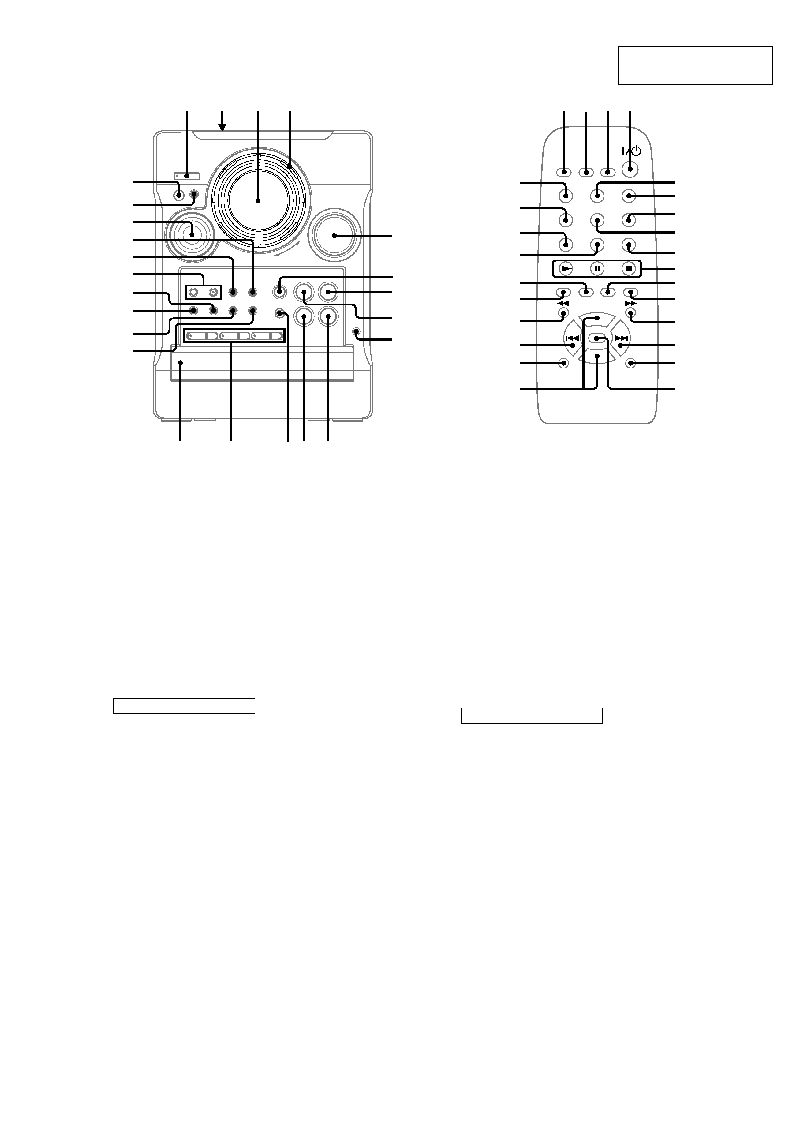
123
4
5
wd
wf
6
7
8
9
0
qa
qs
qd
qf
qh
qg
qj
ql
ws
w;
wa
qk
BASS/TREBLE ws (21)
CD 1 3 qd (11)
CD 1 3 Z qd (9)
CD disc tray qf (9)
CD SYNC ql (18)
CD NX 8 (9)
DBFB wa (20)
DIMMER qg (7)
DISPLAY wd (8, 12)
Display window 3
EDIT w; (18)
FUNCTION qs (9, 17, 18)
GROOVE qj (20)
MD 0 (24)
MUSIC MENU ws (21)
PHONES jack 9
PLAY MODE/DIRECTION qk
(9, 17, 18)
REC PAUSE/START ql (18, 19)
Remote sensor wf
REPEAT qh (10)
STEREO/MONO qh (15)
Tape deck lid 2 (17)
TAPE nN qa (17, 18)
TUNER/BAND 7 (14, 15)
VOLUME 5
BUTTON DESCRIPTIONS
?/1 1
./> 4
x 6
m/M ws
+/ ws
6
7
8
9
5
qf
qg
qh
0
qd
qa
qs
ql
qk
qj
w;
12 3 4
wa
ws
wd
wh
wg
wf
CHECK 8 (11)
CLEAR qs (11)
CLOCK/TIMER SELECT 2
(20, 23)
CLOCK/TIMER SET 3
(8, 19, 22)
DBFB wh (20)
DIMMER wd (7)
DISC SKIP 9 (10, 12)
DISPLAY qk (8, 12)
ENTER/YES qa (8, 13, 14, 19,
22)
FUNCTION qg (9, 17, 18)
GROOVE qh (20)
MENU/NO wa (14)
MUSIC MENU 6 (21)
NAME EDIT/CHARACTER ws
(12, 16)
REPEAT 7 (10)
SCROLL wg (13)
SLEEP 1 (22)
SURROUND 5 (20)
TUNER/BAND wf (14, 15)
VOL +/ qj
BUTTON DESCRIPTIONS
@/1 4
N q;
x q;
X q;
M qd
> qf
. ql
m w;