MICROFILM
SERVICE MANUAL
South African Model
Middle and Near East Model
CD/DVD PLAYER
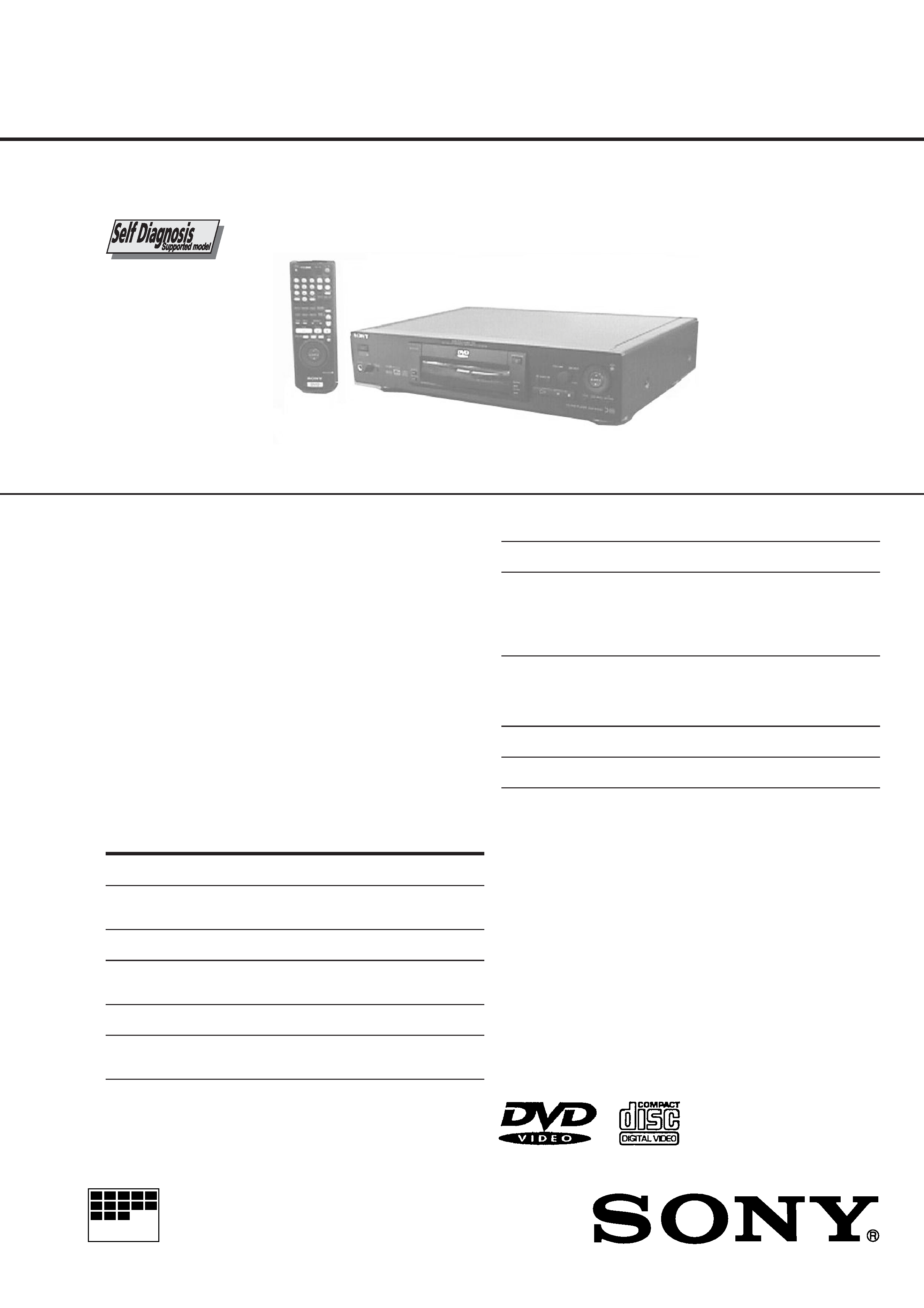
DVP-S525D/S725D
RMT-D108P/D111P
SPECIFICATIONS
Photo: DVP-S725D
CD/DVD player
Laser
Semiconductor laser
Signal format system
PAL/(NTSC)
Audio characteristics
Frequency response
DVD (PCM 96 kHz): 2 Hz to 44 kHz
(±1 dB)* (S525D)
DVD (PCM 96 kHz): 2 Hz to 44 kHz
(±0.5 dB)* (S725D)
DVD (PCM 48 kHz): 2 Hz to 22 kHz
(±0.5 dB)
CD: 2 Hz to 20 kHz (±0.5 dB)
Signal-to-noise ratio
More than 110 dB (LINE OUT (AUDIO)
connectors only) (S525D)
More than 110 dB (AUDIO OUT
connector only) (S725D)
Harmonic distortion
Less than 0.0025%
Dynamic range
More than 100 dB (DVD)
More than 98 dB (CD)
Wow and flutter
Less than detected value
(±0.001% W PEAK)
Outputs and inputs
Jack
Output
Load impedance
type
level
LINE OUT
Phono
2 Vrms
Over 10 kilohms
(AUDIO)
jacks
(at 50 kilohms)
(S525D)
AUIO OUT
Phono
2 Vrms
Over 10 kilohms
(S725D)
jacks
(at 50 kilohms)
DIGITAL OUT
Optical
18 dBm
Wave length: 660 nm
(OPTICAL)
output
connector
DIGITAL OUT
Phono
0.5 Vp-p
75 ohms terminated
(COAXIAL)
jack
LINE OUT
Phono
1.0 Vp-p
75 ohms,
(VIDEO)
jacks
sync negative
(S525D)
VIDEO OUT
Phono
1.0 Vp-p
75 ohms,
(1, 2) (S725D)
jacks
sync negative
S VIDEO OUT
4-pin
Y: 1.0 Vp-p
75 ohms,
(S525D)
mini DIN
sync negative
S VIDEO OUT
C: 0.3 Vp-p
75 ohms terminated
(1, 2) (S725D)
(PAL)
C: 0.286 Vp-p
(NTSC)
COMPONENT
phono
Y: 1.0 Vp-p
75 ohms,
VIDEO OUT
jacks
sync negative
(Y, CB/B-Y,
CB/B-Y,
CR/R-Y)
CR/R-Y:
(S725D)
0.7 Vp-p
75 ohms
PHONES
Phone
12 mW
32 ohms
jack
5.1CH
Phono
2 Vrms
Over 10 kilohms
OUTPUT
jacks
(at 50 kilohms)
General
Power requirements
220 240 V AC, 50/60 Hz
Power consumption
17 W (S525D)
22 W (S725D)
Dimensions (approx.)
430
× 95 × 305 mm (w/h/d)
incl. projecting parts
Mass (approx.)
3.4 kg (S525D)
4.0 kg (S725D)
Operating temperature
5
°C to 35°C
Operating humidity
5% to 90%
Continued on next page
2
WARNING!!
WHEN SERVICING, DO NOT APPROACH THE LASER
EXIT WITH THE EYE TOO CLOSELY. IN CASE IT IS
NECESSARY TO CONFIRM LASER BEAM EMISSION,
BE SURE TO OBSERVE FROM A DISTANCE OF
MORE THAN 25 cm FROM THE SURFACE OF THE
OBJECTIVE LENS ON THE OPTICAL PICK-UP BLOCK.
CAUTION:
The use of optical instrument with this product will increase eye
hazard.
CAUTION
Use of controls or adjustments or performance of procedures
other than those specified herein may result in hazardous ra-
diation exposure.
SAFETY-RELATED COMPONENT WARNING!!
COMPONENTS IDENTIFIED BY MARK
! OR DOTTED
LINE WITH MARK
! ON THE SCHEMATIC DIAGRAMS
AND IN THE PARTS LIST ARE CRITICAL TO SAFE
OPERATION. REPLACE THESE COMPONENTS WITH
SONY PARTS WHOSE PART NUMBERS APPEAR AS
SHOWN IN THIS MANUAL OR IN SUPPLEMENTS PUB-
LISHED BY SONY.
1. Check the area of your repair for unsoldered or poorly-sol-
dered connections. Check the entire board surface for solder
splashes and bridges.
2. Check the interboard wiring to ensure that no wires are
"pinched" or contact high-wattage resistors.
3. Look for unauthorized replacement parts, particularly transis-
tors, that were installed during a previous repair. Point them
out to the customer and recommend their replacement.
SAFETY CHECK-OUT
After correcting the original service problem, perform the following
safety checks before releasing the set to the customer:
4. Look for parts which, though functioning, show obvious signs
of deterioration. Point them out to the customer and recom-
mend their replacement.
5. Check the B+ voltage to see it is at the values specified.
CLASS 3B LASER
LUOKAN 3B LASER
LASERKLASS 3B
Supplied accessories
· Audio/Video connecting cord (1)
· S video cable (1)
· Remote commander (remote) RMT-D108P (1)
(S525D)
· Remote commander (remote) RMT-D111P (1)
(S725D)
· Size AA (R6) batteries (2)
DVP-S525D:
* The signals from LINE OUT (AUDIO) connectors and 5.1 ch L, R
connectors are measured. When you play the PCM sound tracks with
96 kHz sampling frequency, the output signals from the DIGITAL OUT
(OPTICAL, COAXIAL) are converted to 48 kHz (sampling fre-
quency).
DVP-S725D:
* The signals from AUDIO OUT connectors and 5.1 ch L, R connectors
are measured. When you play the PCM sound tracks with 96 kHz
sampling frequency, the output signals from the DIGITAL OUT
(OPTICAL, COAXIAL) are converted to 48 kHz (sampling fre-
quency).
Design and specifications are subject to change without notice.

3
TABLE OF CONTENTS
Section
Title
Page
Section
Title
Page
Service Note ............................................................................ 4
1.
GENERAL
Getting Started .............................................................. 1-1
Playing Discs ................................................................. 1-4
Using Various Functions with the Control Menu ........... 1-6
Settings and Adjustments ............................................. 1-12
2.
DISASSEMBLY
2-1.
Case Removal ............................................................... 2-1
2-2.
MB-85 Board Removal .................................................. 2-1
2-3.
Power Block Removal ................................................... 2-1
2-4.
ER-4/5 Board Removal ................................................. 2-1
2-5.
AU-209 Board Removal (S525D) ................................. 2-2
2-6.
AU-211 Board Removal (S725D) .................................. 2-2
2-7.
Tray Cover Removal ..................................................... 2-2
2-8.
Front Panel Removal .................................................... 2-2
2-9.
Mechanism Deck Removal ........................................... 2-3
2-10. Tray Removal ................................................................ 2-3
2-11. Optical Pick-up Removal ............................................... 2-3
2-12. Belt, Loading Motor (M001),
MS-29/TK-54 Board Removal ....................................... 2-3
2-13. Internal View .................................................................. 2-4
2-14. Circuit Boards Location ................................................. 2-5
3.
BLOCK DIAGRAMS
3-1.
Overall Block Diagram .................................................. 3-1
3-2.
RF/Servo Block Diagram .............................................. 3-3
3-3.
Signal Process Block Diagram ..................................... 3-5
3-4.
Video Block Diagram ..................................................... 3-7
3-5.
System Control Block Diagram ..................................... 3-9
3-6.
Audio (1) Block Diagram ............................................... 3-11
3-7.
Audio (2) Block Diagram ............................................... 3-13
3-8.
Audio (3) Block Diagram ............................................... 3-15
3-9.
Interface Control Block Diagram ................................... 3-17
3-10. Power Block Diagram .................................................... 3-19
4.
PRINTED WIRING BOARDS AND SCHEMATIC
DIAGRAMS
4-1.
Frame Schematic Diagrams .......................................... 4-3
FRAME (1) Schematic Diagram .................................... 4-3
FRAME (2) Schematic Diagram .................................... 4-5
FRAME (3) Schematic Diagram .................................... 4-7
4-2.
Printed Wiring Boards and Schematic Diagrams ......... 4-9
TK-54 Printed Wiring Board .......................................... 4-9
TK-54 Schematic Diagram ............................................ 4-13
MS-29 Printed Wiring Board and
Schematic Diagram ....................................................... 4-15
MB-85 Printed Wiring Board ......................................... 4-17
MB-85 (AV DECODER) Schematic Diagram ................ 4-21
MB-85 (SDRAM) Schematic Diagram .......................... 4-23
MB-85 (SERVO DSP) Schematic Diagram .................. 4-25
MB-85 (DRIVE) Schematic Diagram ............................ 4-27
MB-85 (ARP) Schematic Diagram ................................ 4-29
MB-85 (SYSTEM CONTROL)
Schematic Diagram ....................................................... 4-31
MB-85 (HGA) Schematic Diagram ................................ 4-33
MB-85 (CLOCK GENERATOR, AUDIO DSP,
V EQ/NR) Schematic Diagram ...................................... 4-35
MB-85 (DAC) Schematic Diagram ................................ 4-37
MB-85 (BIAS) Schematic Diagram ............................... 4-39
AU-211 Printed Wiring Board ........................................ 4-41
AU-211 (AUDIO) Schematic Diagram ........................... 4-45
AU-211 (VIDEO BUFFER) Schematic Diagram ........... 4-47
AU-209 Printed Wiring Board ....................................... 4-49
AU-209 (AUDIO) Schematic Diagram .......................... 4-51
AU-209 (VIDEO BUFFER) Schematic Diagram ........... 4-53
ER-4 Printed Wiring Board ............................................ 4-55
ER-4 (EURO AV1) Schematic Diagram ........................ 4-57
ER-4 (EURO AV2) Schematic Diagram ........................ 4-59
ER-5 Printed Wiring Board ............................................ 4-61
ER-5 (EURO AV1) Schematic Diagram ........................ 4-65
ER-5 (EURO AV2) Schematic Diagram ........................ 4-67
FL-100 Printed Wiring Board ........................................ 4-69
FL-98 Printed Wiring Board .......................................... 4-73
FL-98/100 (FUNCTION SWITCH)
Schematic Diagram ....................................................... 4-75
FL-98/100 (IF CON) Schematic Diagram ..................... 4-77
SW-314/316 Printed Wiring Boards .............................. 4-79
FR-147/149 Printed Wiring Boards ............................... 4-80
SW-314/316, FR-147/149 Schematic Diagram ............ 4-81
HP-108/110 Printed Wiring Boards and
Schematic Diagram ....................................................... 4-83
RY-12 Printed Wiring Board and
Schematic Diagram ....................................................... 4-85
HS-030SH Printed Wiring Board .................................. 4-87
HS-030SH Schematic Diagram .................................... 4-89
5.
IC PIN FUNCTION DESCRIPTION
5-1.
System Control Pin Function
(MB-85 Board IC202) .................................................... 5-1
6.
TEST MODE
6-1.
General Description ...................................................... 6-1
6-2.
Starting Test Mode ........................................................ 6-1
6-3.
Syscon Diagnosis .......................................................... 6-1
6-4.
Drive Auto Adjustment .................................................. 6-5
6-5.
Drive Manual Operation ................................................ 6-7
6-6.
Mecha Aging ................................................................. 6-9
6-7.
Emergency History ........................................................ 6-9
6-8.
Version Information ....................................................... 6-10
6-9.
Video Level Adjustment ................................................ 6-10
6-10. If Con Self Diagnostic Function .................................... 6-11
7.
ELECTRICAL ADJUSTMENT
7-1.
Power Supply Adjustment ............................................. 7-1
1.
HS030SH Board ............................................................ 7-1
7-2.
Adjustment of Video System ......................................... 7-2
1.
Video Level Adjustment ................................................. 7-2
2.
S-terminal Output Check ............................................... 7-2
3.
Checking Component Video Output B-Y ...................... 7-2
4.
Checking Component Video Output R-Y ...................... 7-2
5.
Checking Component Video Output Y .......................... 7-3
6.
Checking RGB Output R ............................................... 7-3
7.
Checking RGB Output G ............................................... 7-3
8.
Checking RGB Output B ............................................... 7-3
9.
Checking S Video output S-C ....................................... 7-4
7-3.
Adjustment Related Parts Arrangement ....................... 7-6
8.
REPAIR PARTS LIST
8-1.
Exploded Views ............................................................. 8-1
8-1-1. Case Assembly (S525D) .......................................... 8-1
8-1-2. Case Assembly (S725D) .......................................... 8-2
8-1-3. Front Panel Assembly .............................................. 8-3
8-1-4. Chassis Assembly .................................................... 8-4
8-1-5. Mechanism Deck Assembly ..................................... 8-6
8-2.
Electrical Parts List ........................................................ 8-7
4
SERVICE NOTE
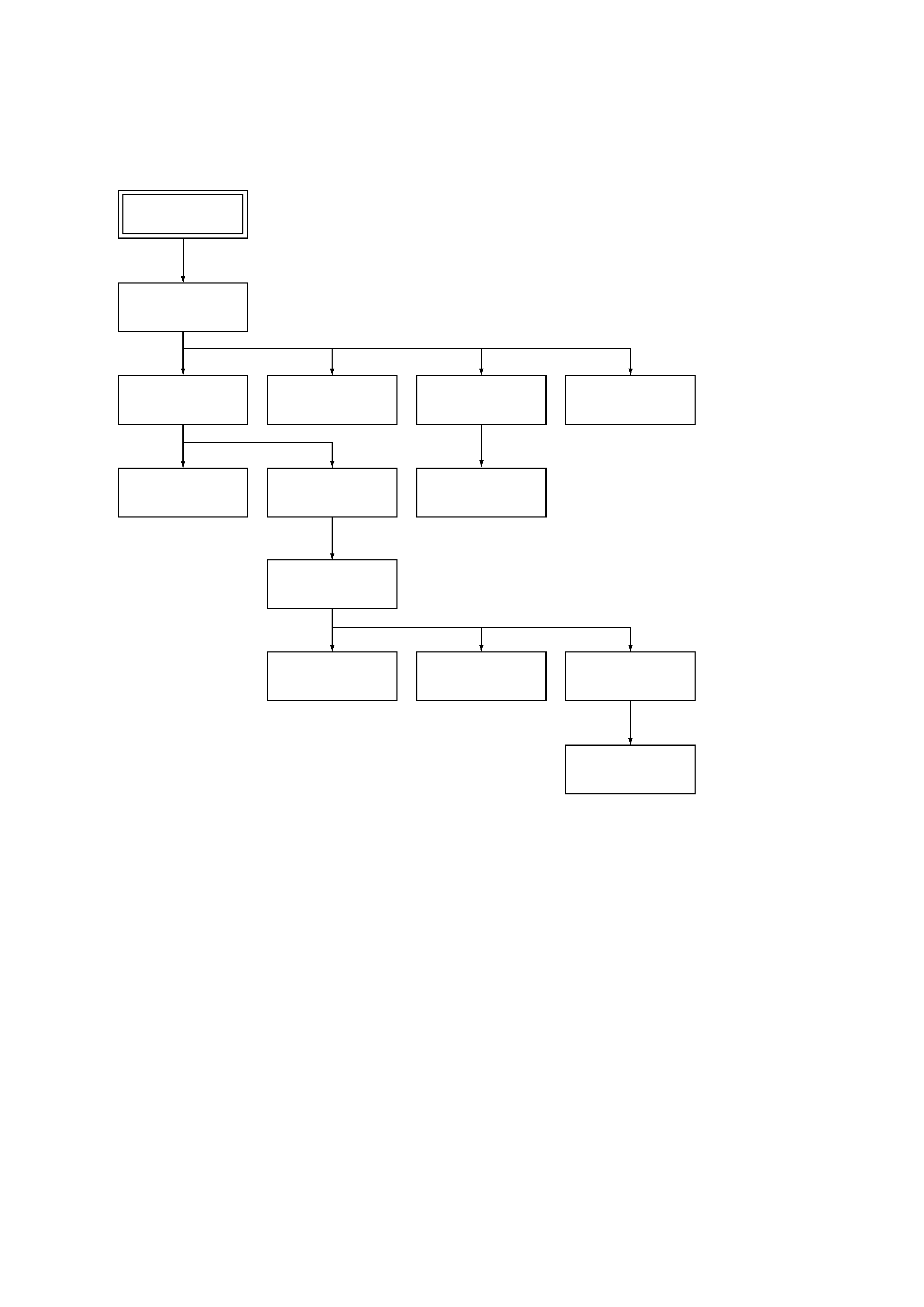
1.
DISASSEMBLY
· This set can be disassembled in the order shown below.
Set
Case
(Page 2-1)
Power Block
(Page 2-1)
ER-4/5 Board
(Page 2-1)
AU-209/211 Board
(Page 2-2)
Mechanism Deck
(Page 2-3)
Front Panel
(Page 2-2)
Tray Cover
(Page 2-2)
Optical Pick-up
(Page 2-3)
Belt
(Page 2-3)
Loading Motor (M001),
MS-29 Board
(Page 2-3)
Tray
(Page 2-3)
MB-85 Board
(Page 2-1)
TK-54 Board
(Page 2-3)
5
4.
HOW TO SERVICE MB-85 BOARD
1) Remove the case from the set. (Refer to 2-1)
2) Remove the MB-85 board. (Refer to 2-2)
3) Set the MB-85 board as shown in Fig. 3.
Note: Do not disconnect wiring, except FMA-7/8/9.
Fig. 3
2.
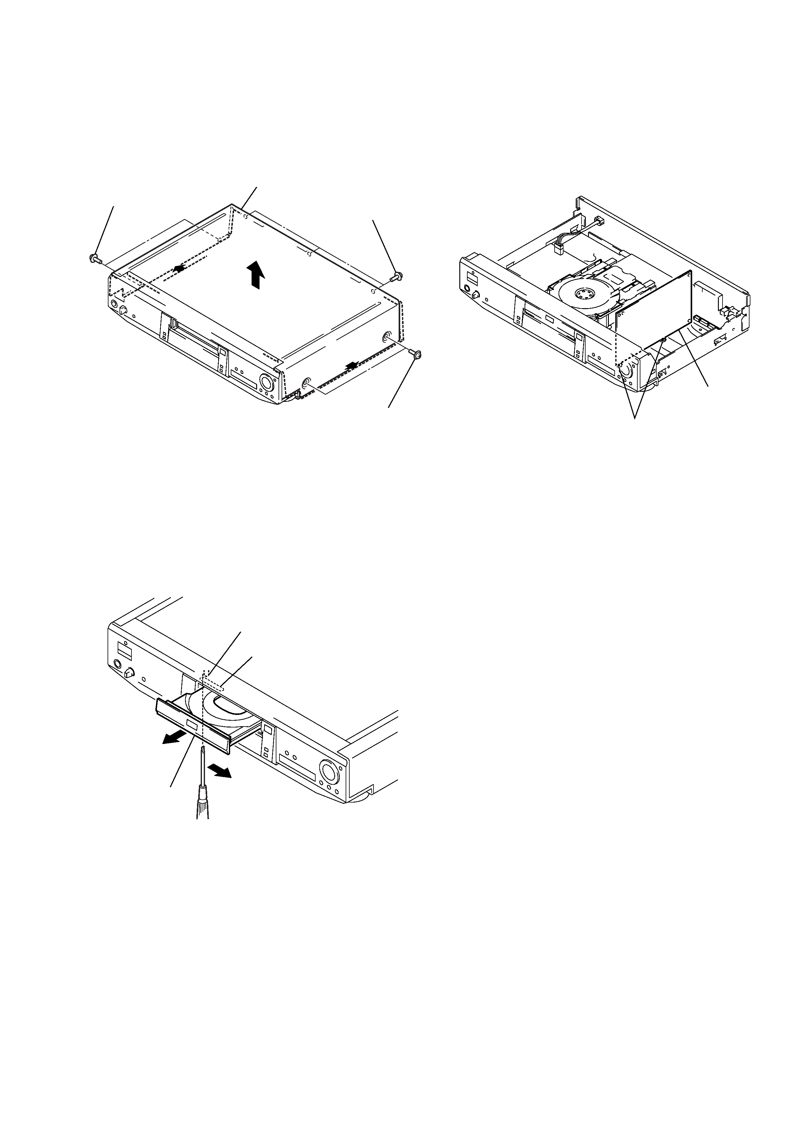
NOTE ON REMOVE THE CASE
1) Remove seven screws. (See Fig. 1)
2) Open the side of case. (See Fig. 1)
3) Remove the case as lift straight. (See Fig. 1)
Fig. 1
3.
DISC REMOVAL PROCEDURE
(at POWER OFF)
1) Insert a tapering driver into the aperture of the unit bottom,
and move the lever of chuck cam in the direction of the arrow
A
. (See Fig. 2)
2) Draw out the tray in the direction of the arrow B, and remove
a disc. (See Fig. 2)
Fig. 2
Two screws
Three screws
Case
Two screws
Lever of chuck cam
Aperture
Tray
A
B
MB-85 board
grooves