SERVICE MANUAL
US Model
Canadian Model
CD/DVD PLAYER
DVP-CX875P
RMT-D149A
SPECIFICATIONS
System
Laser: Semiconductor laser
Signal format system: NTSC
Audio characteristics
Frequency response: DVD VIDEO (PCM
96 kHz): 2 Hz to 44 kHz (
±1.0 dB)/DVD
VIDEO (PCM 48 kHz): 2 Hz to 22 kHz
(
±0.5 dB)/CD: 2 Hz to 20 kHz (±0.5 dB)
Signal-to-noise ratio (S/N ratio): 115 dB
(AUDIO OUTPUT L/R 1/2 jacks only)
Harmonic distortion: 0.003 %
Dynamic range: DVD VIDEO: 103 dB/CD:
99 dB
Wow and flutter: Less than detected value
(
±0.001% W PEAK)
When you play PCM sound tracks with a
96 kHz sampling frequency, the output
signals from the DIGITAL OUTPUT
(COAXIAL or OPTICAL) jack are converted
to 48 kHz sampling frequency.
Outputs
(Jack name: Jack type/Output level/Load
impedance)
AUDIO OUTPUT L/R 1/2: Phono jack/
2Vrms/10 kilohms
DIGITAL OUTPUT (OPTICAL): Optical
output jack/18 dBm (wave length:
660 nm)
DIGITAL OUTPUT (COAXIAL): Phono
jack/0.5 Vp-p/75 ohms
COMPONENT VIDEO OUTPUT (Y, PB,
PR): Phono jack/Y: 1.0 Vp-p/PB, PR:
interlace = 0.648 Vp-p, progressive =
0.7 Vp-p/75 ohms
VIDEO OUTPUT 1/2: Phono jack/
1.0 Vp-p/75 ohms
S VIDEO OUPUT 1/2: 4-pin mini DIN/
Y: 1.0 Vp-p/C: 0.286 Vp-p /75 ohms
S-LINK (CONTROL S IN): Mini jack
General
Power requirements:
120 V AC, 60 Hz
Power consumption: 17 W
Dimensions (approx.): 430
× 158 × 415 mm
(17
× 6 1/4 × 16 3/8 in.) (width/height/
depth) incl. projecting parts
Mass (approx.): 6.9 kg (15 lb 3 oz)
Operating temperature: 5
°C to 35 °C
(41 °F to 95 °F)
Operating humidity: 25 % to 80 %
Supplied accessories
Check that you have the following items:
·Audio/video cord (pinplug
× 3 y pinplug
× 3) (1)
·Remote commander (remote) (1)
·Size AA (R6) batteries (2)
Specifications and design are subject to
change without notice.
ENERGY STARR is a U.S. registered mark.
As an
ENERGY STARR Partner, Sony
Corporation has determined that this product
meets the
ENERGY STARR guidelines for
energy efficiency.
2
WARNING!!
WHEN SERVICING, DO NOT APPROACH THE LASER
EXIT WITH THE EYE TOO CLOSELY. IN CASE IT IS
NECESSARY TO CONFIRM LASER BEAM EMISSION,
BE SURE TO OBSERVE FROM A DISTANCE OF
MORE THAN 25 cm FROM THE SURFACE OF THE
OBJECTIVE LENS ON THE OPTICAL PICK-UP BLOCK.
CAUTION:
The use of optical instrument with this product will increase eye
hazard.
CAUTION
Use of controls or adjustments or performance of procedures
other than those specified herein may result in hazardous ra-
diation exposure.
ATTENTION AU COMPOSANT AYANT RAPPORT
À LA SÉCURITÉ!
LES COMPOSANTS IDENTIFIÉS PAR UNE MARQUE 0
SUR LES DIAGRAMMES SCHÉMATIQUES ET LA LISTE
DES PIÈCES SONT CRITIQUES POUR LA SÉCURITÉ
DE FONCTIONNEMENT. NE REMPLACER CES COM-
POSANTS QUE PAR DES PIÈCES SONY DONT LES
NUMÉROS SONT DONNÉS DANS CE MANUEL OU
DANS LES SUPPLÉMENTS PUBLIÉS PAR SONY.
SAFETY-RELATED COMPONENT WARNING!!
COMPONENTS IDENTIFIED BY MARK 0 OR DOTTED
LINE WITH MARK 0 ON THE SCHEMATIC DIAGRAMS
AND IN THE PARTS LIST ARE CRITICAL TO SAFE
OPERATION. REPLACE THESE COMPONENTS WITH
SONY PARTS WHOSE PART NUMBERS APPEAR AS
SHOWN IN THIS MANUAL OR IN SUPPLEMENTS PUB-
LISHED BY SONY.
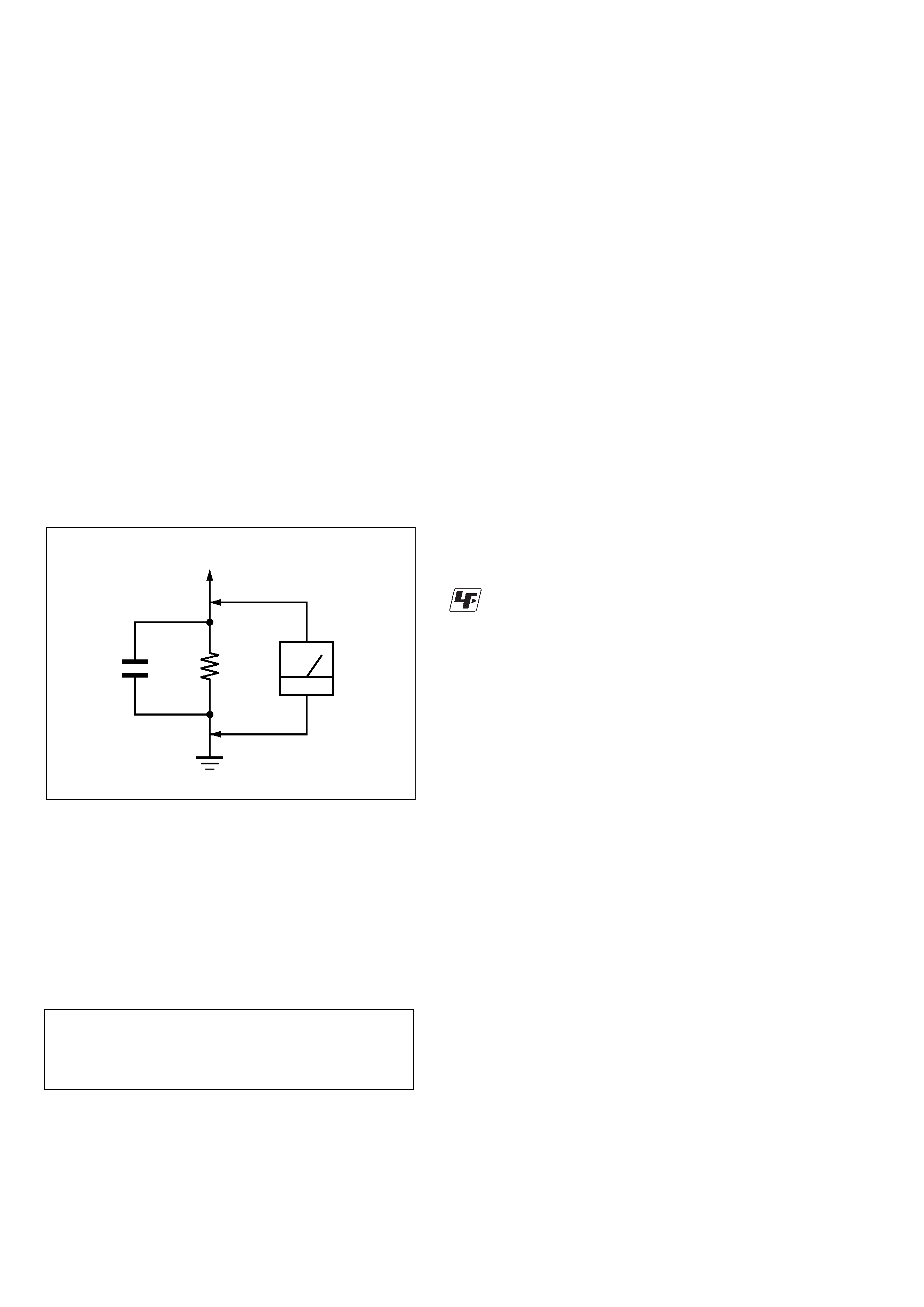
Fig. A.
Using an AC voltmeter to check AC leakage.
1.5 k
0.15 µF
AC
voltmeter
(0.75 V)
To Exposed Metal
Parts on Set
Earth Ground
LEAKAGE TEST
The AC leakage from any exposed metal part to earth ground
and from all exposed metal parts to any exposed metal part having
a return to chassis, must not exceed 0.5 mA (500 microamperes).
Leakage current can be measured by any one of three methods.
1. A commercial leakage tester, such as the Simpson 229 or RCA
WT-540A. Follow the manufacturers' instructions to use these
instruments.
2. A battery-operated AC milliammeter. The Data Precision 245
digital multimeter is suitable for this job.
3. Measuring the voltage drop across a resistor by means of a
VOM or battery-operated AC voltmeter. The "limit" indica-
tion is 0.75V, so analog meters must have an accurate low-
voltage scale. The Simpson 250 and Sanwa SH-63Trd are ex-
amples of a passive VOM that is suitable. Nearly all battery
operated digital multimeters that have a 2V AC range are suit-
able. (See Fig. A)
1. Check the area of your repair for unsoldered or poorly-sol-
dered connections. Check the entire board surface for solder
splashes and bridges.
2. Check the interboard wiring to ensure that no wires are
"pinched" or contact high-wattage resistors.
3. Look for unauthorized replacement parts, particularly transis-
tors, that were installed during a previous repair. Point them
out to the customer and recommend their replacement.
4. Look for parts which, though functioning, show obvious signs
of deterioration. Point them out to the customer and recom-
mend their replacement.
5. Check the line cord for cracks and abrasion. Recommend the
replacement of any such line cord to the customer.
6. Check the B+ voltage to see it is at the values specified.
7. Check the antenna terminals, metal trim, "metallized" knobs,
screws, and all other exposed metal parts for AC leakage.
Check leakage as described below.
SAFETY CHECK-OUT
After correcting the original service problem, perform the following
safety checks before releasing the set to the customer:
Unleaded solder
Boards requiring use of unleaded solder are printed with the lead-
free mark (LF) indicating the solder contains no lead.
(Caution: Some printed circuit boards may not come printed with
the lead free mark due to their particular size.)
: LEAD FREE MARK
Unleaded solder has the following characteristics.
· Unleaded solder melts at a temperature about 40
°C higher than
ordinary solder.
Ordinary soldering irons can be used but the iron tip has to be
applied to the solder joint for a slightly longer time.
Soldering irons using a temperature regulator should be set to
about 350
°C.
Caution: The printed pattern (copper foil) may peel away if the
heated tip is applied for too long, so be careful!
· Strong viscosity
Unleaded solder is more viscous (sticky, less prone to flow) than
ordinary solder so use caution not to let solder bridges occur
such as on IC pins, etc.
· Usable with ordinary solder
It is best to use only unleaded solder but unleaded solder may
also be added to ordinary solder.

3
TABLE OF CONTENTS
Section
Title
Page
Section
Title
Page
Service Note ............................................................................ 5
1.
GENERAL
Precautions ................................................................... 1-1
Index to Parts and Controls .......................................... 1-2
Simple Start Guide ........................................................ 1-3
Hookups ........................................................................ 1-5
Playing Discs ................................................................. 1-7
Searching for and Managing Discs (Disc Explorer) ..... 1-12
Searching for a Scene ................................................... 1-15
Viewing Information About the Disc .............................. 1-16
Sound Adjustments ....................................................... 1-17
Enjoying Movies ............................................................ 1-18
Using Various Additional Functions .............................. 1-19
Settings and Adjustments ............................................. 1-21
Additional Information ................................................... 1-23
2.
DISASSEMBLY
2-1.
Upper Case Removal .................................................... 2-1
2-2.
Front Panel Block Removal ........................................... 2-1
2-3.
Power Block Removal ................................................... 2-1
2-4.
Mechanism Deck Assembly Removal ........................... 2-1
2-5.
AV-66 Board Removal ................................................... 2-2
2-6.
VD-33 Board Removal .................................................. 2-2
2-7.
MB-107 Board Removal ................................................ 2-2
2-8.
T Driving Block Removal ............................................... 2-2
2-9.
AI-25 Board Removal .................................................... 2-3
2-10. Center Guide Assembly Removal ................................. 2-3
2-11. Mechanism Deck Block Removal .................................. 2-3
2-12. Optical Pick-up Removal ............................................... 2-3
2-13. Circuit Boards Location ................................................. 2-4
3.
BLOCK DIAGRAMS
3-1.
Overall Block Diagram ................................................... 3-1
3-2.
RF/Servo Block Diagram ............................................... 3-3
3-3.
Signal Processor Block Diagram .................................. 3-5
3-4.
System Control Block Diagram ..................................... 3-7
3-5.
Video Block Diagram ..................................................... 3-9
3-6.
Audio Block Diagram ..................................................... 3-11
3-7.
NAND FLASH/300 CHG MECHA Control
Block Diagram ............................................................... 3-13
3-8.
Interface Control Block Diagram ................................... 3-15
3-9.
Power (1) Block Diagram .............................................. 3-17
3-10. Power (2) Block Diagram .............................................. 3-19
4.
PRINTED WIRING BOARDS AND SCHEMATIC
DIAGRAMS
4-1.
Frame Schematic Diagram ............................................ 4-3
4-2.
Printed Wiring Boards and Schematic Diagrams ......... 4-7
TK-63 (RELAY) Printed Wiring Board
and Schematic Diagram ................................................ 4-7
MB-107 Printed Wiring Board ....................................... 4-9
MB-107 (RF AMP, SERVO) Schematic Diagram .......... 4-13
MB-107 (ARP, SERVO DSP) Schematic Diagram ........ 4-15
MB-107 (AV DECODER) Schematic Diagram .............. 4-17
MB-107 (MOTOR DRIVE) Schematic Diagram ............ 4-19
MB-107 (SYSTEM CONTROL)
Schematic Diagram ....................................................... 4-21
MB-107 (CLOCK GENERATOR)
Schematic Diagram ....................................................... 4-23
MB-107 (I/P CONVERTOR) Schematic Diagram ......... 4-25
MB-107 (VIDEO ENCODER) Schematic Diagram ....... 4-27
MB-107 (AUDIO D/A CONVERTER)
Schematic Diagram ....................................................... 4-29
MB-107 (NAND FLASH I/F, EXTENSION I/O)
Schematic Diagram ....................................................... 4-31
AI-25 Printed Wiring Board ........................................... 4-33
AI-25 (LOADING/TURN TABLE/DOOR MOTOR
DRIVE, INTERFACE) Schematic Diagram ................... 4-35
VD-33 Printed Wiring Board .......................................... 4-37
VD-33 (VIDEO BUFFER) Schematic Diagram ............. 4-39
AV-66 Printed Wiring Board .......................................... 4-41
AV-66 (AUDIO AMP) Schematic Diagram .................... 4-43
FR-189 Printed Wiring Board ........................................ 4-45
FR-189 (INTERFACE CONTROL)
Schematic Diagram ....................................................... 4-47
CK-118 Printed Wiring Board ........................................ 4-49
CK-118 (DISC SENSOR) Schematic Diagram ............. 4-51
CS-58 Printed Wiring Board .......................................... 4-49
CS-58 (CHUCKING SENSOR) Schematic Diagram .... 4-51
LC-78 Printed Wiring Board .......................................... 4-49
LC-78 (LOADING/CHUCKING MOTOR)
Schematic Diagram ....................................................... 4-51
LS-62 Printed Wiring Board .......................................... 4-49
LS-62 (LOADING SENSOR) Schematic Diagram ........ 4-51
LL-12 Printed Wiring Board ........................................... 4-49
LL-12 (LOADING GUIDE INDICATOR L)
Schematic Diagram ....................................................... 4-51
LR-17 Printed Wiring Board .......................................... 4-49
LR-17 (LOADING GUIDE INDICATOR R)
Schematic Diagram ....................................................... 4-51
FL-128 Printed Wiring Board ........................................ 4-53
FL-128 (FUNCTION SWITCH) Schematic Diagram .... 4-55
SW-374 Printed Wiring Board ....................................... 4-53
SW-374 (EJECT SWITCH) Schematic Diagram .......... 4-55
TS-154 Printed Wiring Board ........................................ 4-57
TS-154 (TURN TABLE SENSOR)
Schematic Diagram ....................................................... 4-59
TM-129 Printed Wiring Board ....................................... 4-57
TM-129 (TURN TABLE MOTOR)
Schematic Diagram ....................................................... 4-59
DA-32 Printed Wiring Board .......................................... 4-57
DA-32 (DOOR SENSOR) Schematic Diagram ............. 4-59
DM-105 Printed Wiring Board ....................................... 4-57
DM-105 (DOOR MOTOR) Schematic Diagram ............ 4-59
ZSSR113M Printed Wiring Board ................................. 4-61
ZSSR113M (SWITCHING REGULATOR)
Schematic Diagram ....................................................... 4-63
5.
IC PIN FUNCTION DESCRIPTION
5-1.
System Control Pin Function
(MB-107 Board IC104) .................................................. 5-1
6.
TEST MODE
6-1.
General Description ...................................................... 6-1
6-2.
Starting Test Mode ........................................................ 6-1
6-3.
Syscon Diagnosis .......................................................... 6-1
6-4.
Drive Auto Adjustment .................................................. 6-6
6-5.
Drive Manual Operation ................................................ 6-8
6-6.
Mecha Aging ................................................................. 6-13
6-7.
Emergency History ........................................................ 6-13
6-8.
Version Information ....................................................... 6-13
6-9.
Video Level Adjustment ................................................ 6-13
6-10. IF CON Self Diagnostic Function .................................. 6-14
6-11. Troubleshooting ............................................................. 6-23
7.
ELECTRICAL ADJUSTMENT
7-1.
Power Supply Check ..................................................... 7-1
1.
ZSSR113M Board ......................................................... 7-1
7-2.
Adjustment of Video System ......................................... 7-2
1.
Video Level Adjustment ................................................ 7-2
2.
Component Video Output Level Adjustment ................. 7-2
3.
Checking S Video Output S-Y ....................................... 7-2
4.
Checking S Video Output S-C ....................................... 7-2

4
Section
Title
Page
5.
Checking Component Video Output Y .......................... 7-3
6.
Checking Component Video Output B-Y ...................... 7-3
7.
Checking Component Video Output R-Y ...................... 7-3
7-3. Adjustment Related Parts Arrangement ....................... 7-6
8.
REPAIR PARTS LIST
8-1.
Exploded Views ............................................................. 8-1
8-1-1. Case Assembly ........................................................ 8-1
8-1-2. Front Panel Assembly-1 ........................................... 8-2
8-1-3. Front Panel Assembly-2 ........................................... 8-3
8-1-4. Chassis Assembly-1 ................................................. 8-4
8-1-5. Chassis Assembly-2 ................................................. 8-5
8-1-6. Chassis Assembly-3 ................................................. 8-6
8-1-7. Mechanism Deck Assembly-1 .................................. 8-7
8-1-8. Mechanism Deck Assembly-2 .................................. 8-8
8-2.
Electrical Parts List ....................................................... 8-9
5
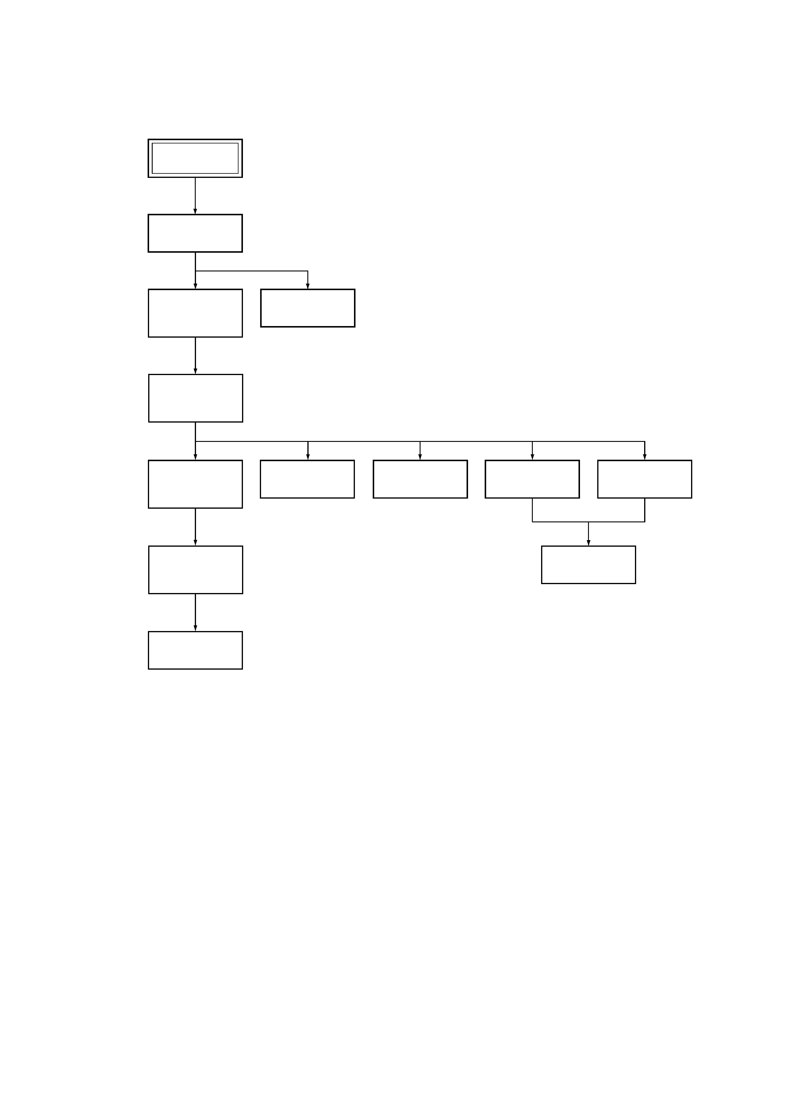
SERVICE NOTE
1.
DISASSEMBLY
·This set can be disassembled in the order shown below.
Set
Upper Case
(Page 2-1)
Power Block
(Page 2-1)
Optical Pick-Up
(Page 2-3)
VD-33 Board
(Page 2-2)
AV-66 Board
(Page 2-2)
AI-25 Board
(Page 2-3)
MB-107 board
(Page 2-2)
T Driving Block
(Page 2-2)
Mechanical Deck
Assembly
(Page 2-1)
Mechanical Deck
Block
(Page 2-3)
Center Guide
Assembly
(Page 2-3)
Front Panel Block
Removal
(Page 2-1)