MICROFILM
SERVICE MANUAL
US Model
Canadian Model
E Model
DVP-C650D
PX Model
DVP-C653D
CD/DVD PLAYER
DVP-C650D/C653D
RMT-D112A
SPECIFICATIONS
CD/DVD player
Laser
Semiconductor laser
Signal format system
NTSC
Audio characteristics
Frequency response
DVD (PCM 96 kHz): 2 Hz to 44 kHz
(±1 dB)*
DVD (PCM 48 kHz): 2 Hz to 22 kHz
(±0.5 dB)
CD: 2 Hz to 20 kHz (±0.5 dB)
Signal-to-noise ratio
More than 115 dB (LINE OUT (AUDIO 1,
2) connectors only)
Harmonic distortion
Less than 0.0025%
Dynamic range
More than 100 dB (DVD)
More than 97 dB (CD)
Wow and flutter
Less than detected value
(±0.001% W PEAK)
Outputs and inputs
Jack
Output
Load impedance
type
level
LINE OUT
Phono
2 Vrms
Over 10 kilohms
(AUDIO 1, 2)
jacks
(at 50 kilohms)
DIGITAL OUT
Optical
18 dBm
Wave length: 660 nm
(OPTICAL)
output
connector
DIGITAL OUT
Phono
0.5 Vp-p
75 ohms terminated
(COAXIAL)
jack
LINE OUT
Phono
1.0 Vp-p
75 ohms,
(VIDEO 1, 2)
jacks
sync negative
S VIDEO OUT
4-pin
Y: 1.0 Vp-p
75 ohms,
(1, 2)
mini DIN
sync negative
C: 0.286 Vp-p
75 ohms terminated
COMPONENT
phono
Y: 1.0 Vp-p
75 ohms,
VIDEO OUT
jacks
sync negative
(Y, PB/B-Y,
PB/B-Y,
PR/R-Y)
PR/R-Y:
0.7 Vp-p
75 ohms
PHONES
Phone
12 mW
32 ohms
jack
5.1CH
Phono
2 Vrms
Over 10 kilohms
OUTPUT
jacks
(at 50 kilohms)
Jack
Output
Load impedance
type
level
S-LINK
Mini jack
MEGA
Mini jack
CONTROL
AUDIO IN
Phono
2 Vrms
47 kilohms
jack
General
Power requirements (indicated on the rear panel)
120 V AC, 60 Hz (C650D : US, Canadian)
110240 V AC, 50/60 Hz
(C653D : E, C653D : PX)
Power consumption
18 W
Dimensions (approx.)
430
× 120 × 425 mm
(17
× 43/
4
× 163/
4
in.) (w/h/d)
incl. projecting parts
Mass (approx.)
6.1 kg (13 lb 7 oz)
Operating temperature
41
°F to 95°F (5°C to 35°C)
Operating humidity
5% to 90%
Supplied accessories
· Audio/Video/S-link connecting cord (1) or Audio/Video connecting
cord (1)
· S video cord (1)
· Plug adaptor (1) (except for the USA/Canada models)
· Remote commander (remote) RMT-D112A (1)
· Size AA (R6) batteries (2)
* The signals from LINE OUT (AUDIO 1, 2) connectors and 5.1 ch L, R
connectors are measured. When you play the PCM sound tracks with
96 kHz sampling frequency, the output signals from the DIGITAL OUT
(OPTICAL, COAXIAL) are converted to 48 kHz (sampling frequency).
Design and specifications are subject to change without notice.
Photo: DVP-C650D
2
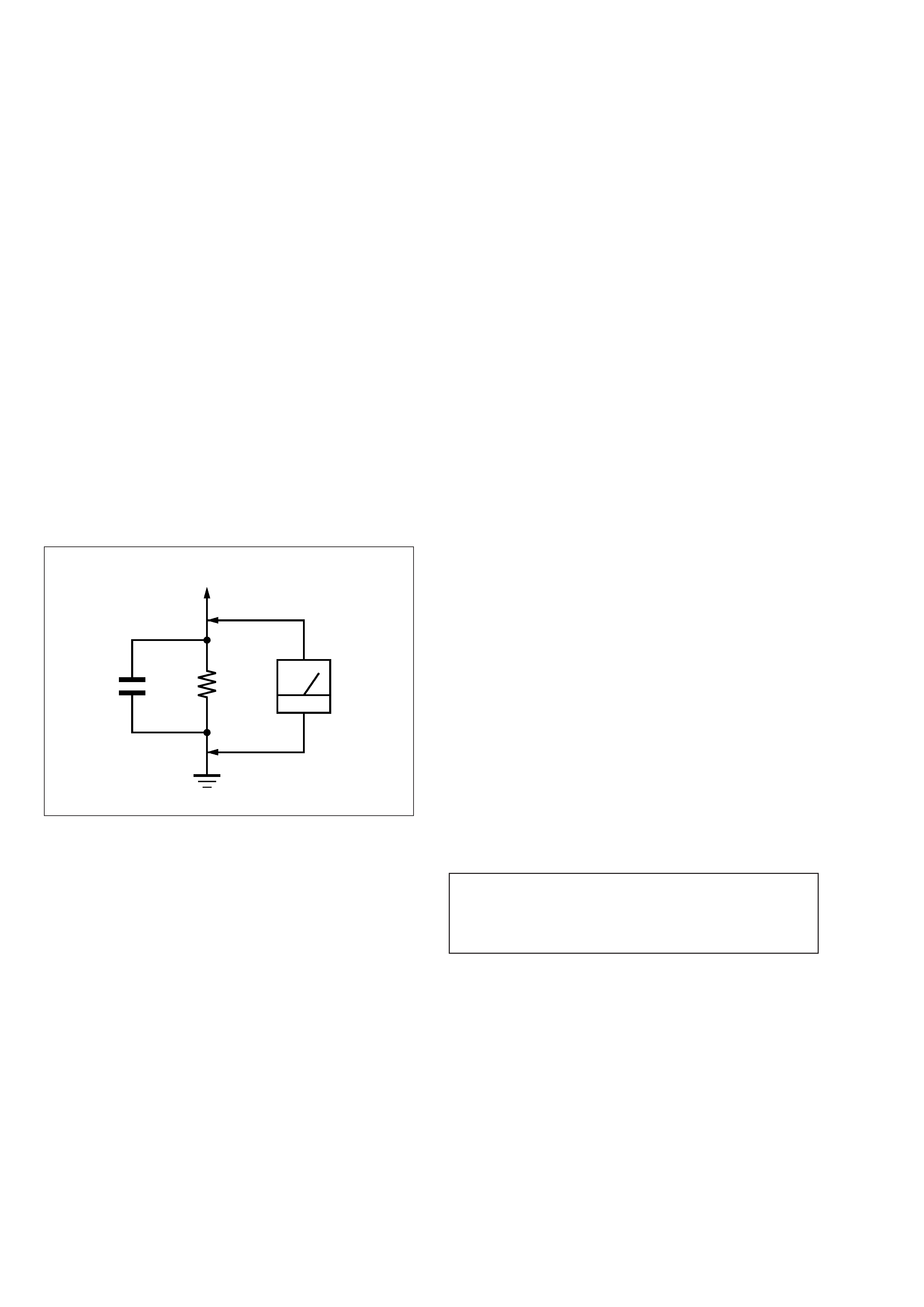
LEAKAGE TEST
The AC leakage from any exposed metal part to earth ground
and from all exposed metal parts to any exposed metal part having
a return to chassis, must not exceed 0.5 mA (500 microamperes).
Leakage current can be measured by any one of three methods.
1. A commercial leakage tester, such as the Simpson 229 or RCA
WT-540A. Follow the manufacturers' instructions to use these
instruments.
2. A battery-operated AC milliammeter. The Data Precision 245
digital multimeter is suitable for this job.
3. Measuring the voltage drop across a resistor by means of a
VOM or battery-operated AC voltmeter. The "limit" indica-
tion is 0.75V, so analog meters must have an accurate low-
voltage scale. The Simpson 250 and Sanwa SH-63Trd are ex-
amples of a passive VOM that is suitable. Nearly all battery
operated digital multimeters that have a 2V AC range are suit-
able. (See Fig. A)
Fig. A
Using AC voltmeter to check AC leakage
1.5 k
0.15
µF
AC
Voltmeter
(0.75 V)
To Exposed Metal
Parts on Set
Earth Ground
WARNING!!
WHEN SERVICING, DO NOT APPROACH THE LASER
EXIT WITH THE EYE TOO CLOSELY. IN CASE IT IS
NECESSARY TO CONFIRM LASER BEAM EMISSION,
BE SURE TO OBSERVE FROM A DISTANCE OF
MORE THAN 25 cm FROM THE SURFACE OF THE
OBJECTIVE LENS ON THE OPTICAL PICK-UP BLOCK.
CAUTION:
The use of optical instrument with this product will increase eye
hazard.
ATTENTION AU COMPOSANT AYANT RAPPORT
À LA SÉCURITÉ!
LES COMPOSANTS IDENTIFIÉS PAR UNE MARQUE
!
SUR LES DIAGRAMMES SCHÉMATIQUES ET LA LISTE
DES PIÈCES SONT CRITIQUES POUR LA SÉCURITÉ
DE FONCTIONNEMENT. NE REMPLACER CES COM-
POSANTS QUE PAR DES PIÈCES SONY DONT LES
NUMÉROS SONT DONNÉS DANS CE MANUEL OU
DANS LES SUPPLÉMENTS PUBLIÉS PAR SONY.
1. Check the area of your repair for unsoldered or poorly-sol-
dered connections. Check the entire board surface for solder
splashes and bridges.
2. Check the interboard wiring to ensure that no wires are
"pinched" or contact high-wattage resistors.
3. Look for unauthorized replacement parts, particularly transis-
tors, that were installed during a previous repair. Point them
out to the customer and recommend their replacement.
4. Look for parts which, though functioning, show obvious signs
of deterioration. Point them out to the customer and recom-
mend their replacement.
5. Check the line cord for cracks and abrasion. Recommend the
replacement of any such line cord to the customer.
6. Check the B+ voltage to see it is at the values specified.
7. Check the antenna terminals, metal trim, "metallized" knobs,
screws, and all other exposed metal parts for AC leakage.
Check leakage as described below.
SAFETY CHECK-OUT
After correcting the original service problem, perform the following
safety checks before releasing the set to the customer:
SAFETY-RELATED COMPONENT WARNING!!
COMPONENTS IDENTIFIED BY MARK
! OR DOTTED
LINE WITH MARK
! ON THE SCHEMATIC DIAGRAMS
AND IN THE PARTS LIST ARE CRITICAL TO SAFE
OPERATION. REPLACE THESE COMPONENTS WITH
SONY PARTS WHOSE PART NUMBERS APPEAR AS
SHOWN IN THIS MANUAL OR IN SUPPLEMENTS PUB-
LISHED BY SONY.
CAUTION
Use of controls or adjustments or performance of procedures
other than those specified herein may result in hazardous ra-
diation exposure.

3
TABLE OF CONTENTS
Section
Title
Page
Section
Title
Page
Service Note ............................................................................ 4
1.
GENERAL
This Player Can Play the Following Discs .................... 1-1
Getting Started .............................................................. 1-1
Playing Discs ................................................................. 1-3
Using Various Functions with the Control Menu ........... 1-6
Settings and Adjustments ............................................. 1-12
Additional Information ................................................... 1-16
2.
DISASSEMBLY
2-1.
Case Removal ............................................................... 2-1
2-2.
Front Panel Section Removal ........................................ 2-1
2-3.
MB-85 Board Removal .................................................. 2-1
2-4.
AU-215 Board Removal ................................................ 2-1
2-5.
Rear Panel Section Removal ........................................ 2-2
2-6.
Table Ass'y Removal ..................................................... 2-2
2-7.
Rotary Motor Ass'y (M951) Removal ............................ 2-2
2-8.
Chassis Ass'y ................................................................ 2-2
2-9.
Loading Motor Ass'y (M991) Removal .......................... 2-3
2-10. BU Holder Ass'y Removal ............................................. 2-3
2-11. TK-53 Board Removal ................................................... 2-3
2-12. Optical Pick-up Removal ............................................... 2-3
2-13. Internal View .................................................................. 2-4
2-14. Circuit Boards Location ................................................. 2-5
3.
BLOCK DIAGRAMS
3-1.
Overall Block Diagram .................................................. 3-1
3-2.
RF/Servo Block Diagram .............................................. 3-3
3-3.
Signal Process/Video Block Diagram ........................... 3-5
3-4.
System Control Block Diagram ..................................... 3-7
3-5.
Audio (1) Block Diagram ............................................... 3-9
3-6.
Audio (2) Block Diagram ............................................... 3-11
3-7.
Interface Control Block Diagram ................................... 3-13
3-8.
Power Block Diagram .................................................... 3-15
4.
PRINTED WIRING BOARDS AND SCHEMATIC
DIAGRAMS
4-1.
Frame Schematic Diagram ........................................... 4-3
4-2.
Printed Wiring Boards and Schematic Diagrams ......... 4-7
TK-53 (RF/SERVO) Printed Wiring Board .................... 4-7
TK-53 (RF/SERVO) Schematic Diagram ...................... 4-11
SE-91 (SENSOR), LE-24 (LED)
Printed Wiring Boards and Schematic Diagram ........... 4-13
MB-85 (SIGNAL PROCESS)
Printed Wiring Board ..................................................... 4-15
MB-85 (AV DECODER) Schematic Diagram ................ 4-19
MB-85 (SDRAM) Schematic Diagram .......................... 4-21
MB-85 (SERVO DSP) Schematic Diagram ................... 4-23
MB-85 (DRIVE) Schematic Diagram ............................ 4-25
MB-85 (ARP) Schematic Diagram ................................ 4-27
MB-85 (SYSTEM CONTROL)
Schematic Diagram ....................................................... 4-29
MB-85 (HGA) Schematic Diagram ................................ 4-31
MB-85 (CLOCK GENERATOR/AUDIO DSP/
V EQ/NR) Schematic Diagram ...................................... 4-33
MB-85 (DAC) Schematic Diagram ................................ 4-35
MB-85 (BIAS) Schematic Diagram ............................... 4-37
AU-215 (AUDIO/VIDEO BUFFER)
Printed Wiring Board ..................................................... 4-39
AU-215 (AUDIO) Schematic Diagram ........................... 4-43
AU-215 (VIDEO BUFFER) Schematic Diagram ........... 4-45
FL-104 (FUNCTION SWITCH/IF CON), SW-321
(FUNCTION SWITCH) and CK-88 (CONNECTION)
Printed Wiring Boards ................................................... 4-47
FL-104 (FUNCTION SWITCH), SW-321 (FUNCTION
SWITCH) and CK-88 (CONNECTION)
Schematic Diagram ....................................................... 4-51
FL-104 (IF CON) Schematic Diagram .......................... 4-53
FR-154 (IR/POWER SWITCH)
Printed Wiring Boards and Schematic Diagram ........... 4-55
HP-114 (HEADPHONE) Printed Wiring Boards
and Schematic Diagram ................................................ 4-57
LM-59 (LOADING MOTOR), CK-81 (DRIVE)
Printed Wiring Boards ................................................... 4-59
LM-59 (LOADING MOTOR), CK-81 (DRIVE)
Schematic Diagram ....................................................... 4-61
HS-034SF (SWITCHING REGULATOR)
Printed Wiring Board ..................................................... 4-63
HS-034SF (SWITCHING REGULATOR)
Schematic Diagram ....................................................... 4-65
HS-034SU (SWITCHING REGULATOR)
Printed Wiring Board ..................................................... 4-67
HS-034SU (SWITCHING REGULATOR)
Schematic Diagram ....................................................... 4-69
5.
IC PIN FUNCTION DESCRIPTION
5-1.
System Control Pin Function
(MB-85 Board IC202) .................................................... 5-1
6.
TEST MODE
6-1.
General Description ...................................................... 6-1
6-2.
Starting Test Mode ........................................................ 6-1
6-3.
Syscon Diagnosis .......................................................... 6-1
6-4.
Drive Auto Adjustment .................................................. 6-5
6-5.
Drive Manual Operation ................................................ 6-7
6-6.
Mecha Aging ................................................................. 6-9
6-7.
Emergency History ........................................................ 6-9
6-8.
Version Information ....................................................... 6-10
6-9.
Video Level Adjustment ................................................ 6-10
7.
ELECTRICAL ADJUSTMENTS
7-1.
Power Supply Adjustment ............................................. 7-1
1.
Power Supply Check
(HS-034SF/034SU BOARD) ......................................... 7-1
7-2.
Adjustment of Video System ......................................... 7-2
1.
Video Level Adjustment (MB-85 BOARD) .................... 7-2
2.
S-terminal Output Check (MB-85 BOARD) .................. 7-2
3.
Checking Component Video Output B-Y
(MB-85 BOARD) ............................................................ 7-2
4.
Checking Component Video Output R-Y
(MB-85 BOARD) ............................................................ 7-2
5.
Checking Component Video Output Y
(MB-85 BOARD) ............................................................ 7-3
6.
Checking S Video Output S-C (MB-85 BOARD) .......... 7-3
7-3.
Adjustment Related Parts Arrangement ....................... 7-4
8.
REPAIR PARTS LIST
8-1.
Exploded Views ............................................................. 8-1
8-1-1. Main Assembly ......................................................... 8-1
8-1-2. Front Panel Assembly .............................................. 8-2
8-1-3. Table Assembly ........................................................ 8-3
8-1-4. Chassis Assembly .................................................... 8-4
8-2.
Electrical Parts List ....................................................... 8-5
4
SERVICE NOTE
1.
DISASSEMBLY
· This set can be disassembled in the order shown below.
2.
NOTE ON REMOVE THE CASE
1) Remove seven tapping screws. (See Fig. 1)
2) Open the side of case. (See Fig. 1)
3) Remove the case as lift straight. (See Fig. 1)
Set
Case
(Page 2-1)
Front panel section
(Page 2-1)
Table ass'y
(Page 2-2)
Rear panel section
(Page 2-2)
MB-85 board
(Page 2-1)
AU-215 board
(Page 2-1)
Rotary motor ass'y
(M951) (Page 2-2)
Chassis ass'y
(Page 2-2)
BU holder ass'y
(Page 2-3)
TK-53 board
(Page 2-3)
Loading motor ass'y
(M991) (Page 2-3)
Optical pick-up
(Page 2-3)
3.
DISC REMOVAL PROCEDURE
(at POWER OFF)
1) Insert a flat-blade screwdriver into a hole at the bottom, and
rotare the cam gear in direction A. (See Fig. 2)
Table
Hole
Cam gear
A
Case
Two tapping screws
Three tapping screws
Two tapping screws
Fig. 1
Fig. 2
5
4.
NOTE ON MOUNTING GEARS
1) Mount the gear (U/D). (See Fig. 3.)
2) Rotate the gear (U/D) in the direction of the arrow.
(down position) (See Fig. 3.)
3) Align triangle marks of the rotary encoder. (See Fig. 4.)
4) Escape the set lever. (See Fig. 4.)
5) Connect the boss of the gear (main) with the groove of the
rotary encoder and mount the gear (main). (See Fig. 4.)
6) Mount the lock lever (See Fig. 5.)
7) Mount the spring (lock lever). (See Fig. 5.)
8) Rotate the gear (main) in the direction of the arrow A by 90
°
turn. (Gear (U/D) is up position.) (See Fig. 6.)
9) Mount the Gear (rev). (See Fig. 6.)
10) Fix three stopper washers on the groove of shafts.
(See Fig. 6.)
Gear (U/D)
Fig. 3
Fig. 5
Fig. 4
Fig. 6
Spring
(lock lever)
Spring
(lock lever)
Lock lever
Lock lever
Gear
(main)
Gear (main)
Set lever
Boss
Groove
Rotary encoder
Align triangle marks.
BU
Shaft
Stopper washer
Gear (rev)
Gear (main)
Gear (U/D)
Two stopper
washers
Groove
**
*
A