SERVICE MANUAL
LEVEL
2
Link
SERVICE NOTE
DISASSEMBLY
BLOCK DIAGRAMS
FRAME SCHEMATIC DIAGRAMS
SCHEMATIC DIAGRAMS
PRINTED WIRING BOARDS
ADJUSTMENTS
REPAIR PARTS LIST
SPECIFICATIONS
SERVICE NOTE
DISASSEMBLY
BLOCK DIAGRAMS
FRAME SCHEMATIC DIAGRAMS
SCHEMATIC DIAGRAMS
PRINTED WIRING BOARDS
ADJUSTMENTS
REPAIR PARTS LIST
SPECIFICATIONS
Link
Revision History
Revision History
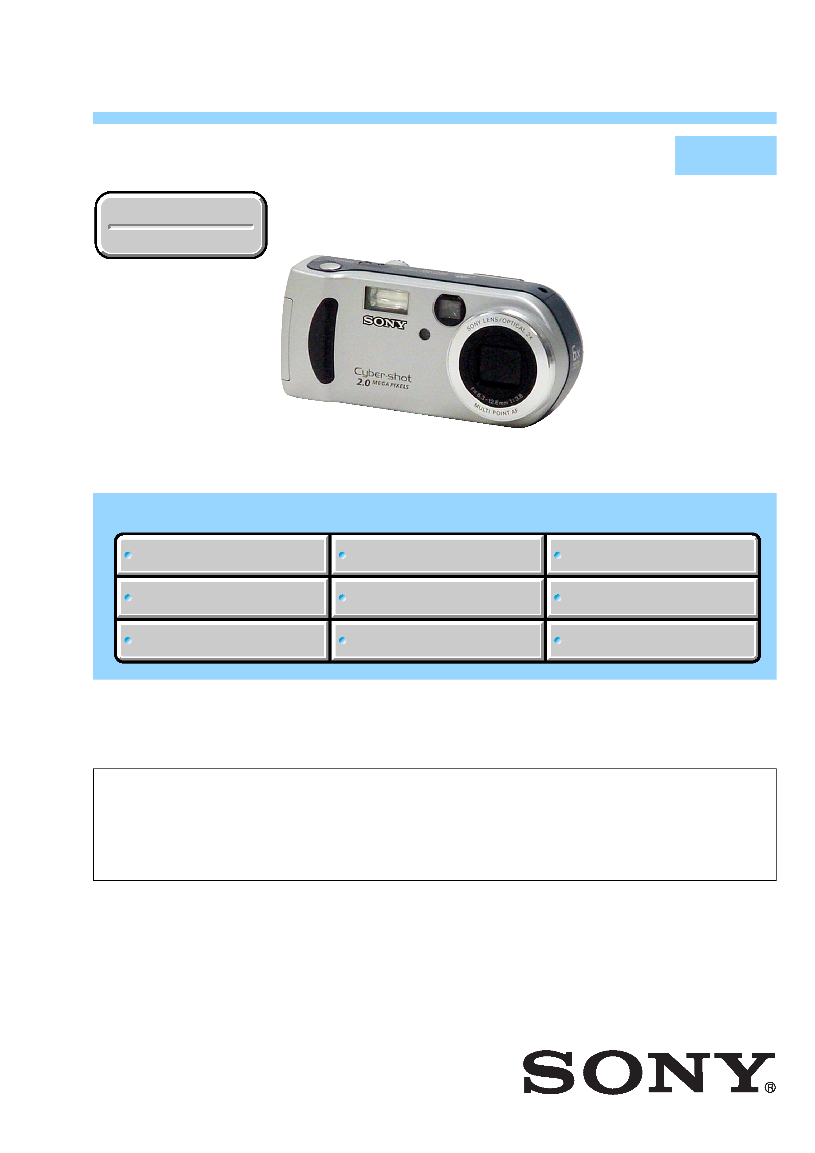
DSC-P51/P51M
On the SY-075 board
This service manual procides the information that is premised
the circuit board replacement service and not intended repair
inside the SY-075 board.
Therefore, schematic diagram, printed wiring board and
electrical parts list of the SY-075 board are not shown.
The following pages are not shown.
SY-075 board
Schematic diagram ......................... Pages 4-11 to 4-26
Printed wiring board ........................ Pages 4-41 to 4-44
Electrical parts list ........................... Pages 6-8 to 6-12
The above-described information is shown in service
manual Level 3.
·For INSTRUCTION MANUAL, refer to separate file (992997071.pdf).
· DSC-P51M is the same as DSC-P51 (US model) except packing materials.
Therefore, information about DSC-P51 (US model) in the text is applied.
· This service manual contains information for Japanese model as well.
US Model
DSC-P51/P51M
Canadian Model
AEP Model
UK Model
E Model
Hong Kong Model
Australian Model
Chinese Model
Korea Model
Tourist Model
Japanese Model
DSC-P51
Ver 1.0 2002. 04
DIGITAL STILL CAMERA
PHOTO DSC-P51

-- 2 --
DSC-P51/P51M
SPECIFICATIONS
COVER
COVER
System
Image device 6.64 mm(1/2.7 type) color
CCD
Primary color filter
Total pixels number of camera
Approx. 2 100 000 pixels
Lens
2
× zoom lens
f=6.3 to 12.6 mm (35 mm camera
conversion: 41to 82 mm), F3.8
Camera
Effective pixels number of camera
Approx. 1 980 000 pixels
Exposure control
Automatic,
Scene Selection (3 mode)
White balanceAutomatic, Daylight, Cloudy,
Fluorescent, Incandescent
Data formats Moving images: MPEG1
Still images: JPEG, GIF (for Clip
Motion)
Recording media
"Memory Stick"
Flash
Recommended distance
0.4 to 2.8 m (1.3 to 9.2 ft) (W/T)
Output connectors
VIDEO OUT jack
Minijack
1 Vp-p, 75 ohm, unbalanced, sync
negative
USB jack
mini-B
LCD screen
LCD panel used
4.0 cm (1.6 type) TFT drive
Total number of dots
61 600 (280
×220) dots
Power, etc.
Power
AA nickel hydride batteries (2)
2.4 V
AC-LS1 AC power adaptor
(not supplied), 4.2 V
Power consumption (when recording)
1.7W
Operating temperature range
0
° to + 40°C (+32° to +104°F)
Storage temperature range
-20
° to + 60°C (-4° to +140°F)
Dimensions
126.9
× 58 × 47 mm (5 × 2 3/8 ×
1 7/8 inches)
Mass
275 g (10 oz) (camera, two batteries,
"Memory Stick" and wrist strap
included)
BC-CS1 Ni-MH battery charger
Power requirements
AC 100 to 240V 50/60Hz
2.2 W
Output voltage
DC 1.8V 180/110 mA
× 2
Dimensions
70
× 29 × 74 mm (2
7/
8 × 1
3/
16 × 3
inches) (W/H/D)
Mass
Approx. 70g (2 oz)
Operating temperature range
0
° to + 40°C (32° to +104°F)
Accessories
·Video connector cable (1)
·R6 (size AA) Ni-MH batteries (2)
·Ni-MH Battery charger (1)
·Power cord (mains lead) (1)
·USB cable (1)
·Wrist strap
·"Memory Stick" (16MB) (1)
·CD-ROM (USB driver: SPVD-008) (1)
·Operating Instructions (1)
Design and specifications are subject to change
without notice.
(W/H/D, protruding portions not
included)
(when ISO sensitivity is set to Auto)

-- 3 --
DSC-P51/P51M
1.
Check the area of your repair for unsoldered or poorly-soldered
connections. Check the entire board surface for solder splashes
and bridges.
2.
Check the interboard wiring to ensure that no wires are
"pinched" or contact high-wattage resistors.
3.
Look for unauthorized replacement parts, particularly
transistors, that were installed during a previous repair. Point
them out to the customer and recommend their replacement.
4.
Look for parts which, through functioning, show obvious signs
of deterioration. Point them out to the customer and
recommend their replacement.
5.
Check the B+ voltage to see it is at the values specified.
6.
Flexible Circuit Board Repairing
·Keep the temperature of the soldering iron around 270°C
during repairing.
· Do not touch the soldering iron on the same conductor of the
circuit board (within 3 times).
· Be careful not to apply force on the conductor when soldering
or unsoldering.
Unleaded solder
Boards requiring use of unleaded solder are printed with the lead-
free mark (LF) indicating the solder contains no lead.
(Caution: Some printed circuit boards may not come printed with
the lead free mark due to their particular size.)
: LEAD FREE MARK
Unleaded solder has the following characteristics.
· Unleaded solder melts at a temperature about 40
°C higher than
ordinary solder.
Ordinary soldering irons can be used but the iron tip has to be
applied to the solder joint for a slightly longer time.
Soldering irons using a temperature regulator should be set to
about 350
°C.
Caution: The printed pattern (copper foil) may peel away if the
heated tip is applied for too long, so be careful!
· Strong viscosity
Unleaded solder is more viscous (sticky, less prone to flow) than
ordinary solder so use caution not to let solder bridges occur such
as on IC pins, etc.
· Usable with ordinary solder
It is best to use only unleaded solder but unleaded solder may
also be added to ordinary solder.
SAFETY CHECK-OUT
After correcting the original service problem, perform the following
safety checks before releasing the set to the customer.
SAFETY-RELATED COMPONENT WARNING!!
COMPONENTS IDENTIFIED BY MARK 0 OR DOTTED LINE WITH
MARK 0 ON THE SCHEMATIC DIAGRAMS AND IN THE PARTS
LIST ARE CRITICAL TO SAFE OPERATION. REPLACE THESE
COMPONENTS WITH SONY PARTS WHOSE PART NUMBERS
APPEAR AS SHOWN IN THIS MANUAL OR IN SUPPLEMENTS
PUBLISHED BY SONY.
ATTENTION AU COMPOSANT AYANT RAPPORT
À LA SÉCURITÉ!
LES COMPOSANTS IDENTIFÉS PAR UNE MARQUE 0 SUR LES
DIAGRAMMES SCHÉMATIQUES ET LA LISTE DES PIÈCES SONT
CRITIQUES POUR LA SÉCURITÉ DE FONCTIONNEMENT. NE
REMPLACER CES COMPOSANTS QUE PAR DES PIÈSES SONY
DONT LES NUMÉROS SONT DONNÉS DANS CE MANUEL OU
DANS LES SUPPÉMENTS PUBLIÉS PAR SONY.
Table for differences of function
Model
DSC-P51
DSC-P51M
(Note)
Destination
US, Canadian, AEP, UK, E,
US
Hong Kong, Australian, Chinese,
Korea, Tourist, Japanese
Note : DSC-P51M is the same as DSC-P51 (US model) except packing materials.
Therefore, information about DSC-P51 (US model) in the text is applied.

-- 4 --
DSC-P51/P51M
TABLE OF CONTENTS
1.
SERVICE NOTE ························································ 1-1
Self-diagnosis Display ····················································· 1-2
2.
DISASSEMBLY
2-1.
Cabinet (Rear) Block Assembly ······································ 2-2
Service Position (CD-391 Board, PK-062 Board,
SY-075 Board: Side B) ···················································· 2-2
2-2.
PK-062 Board ·································································· 2-3
2-3.
LCD Module ···································································· 2-3
2-4.
CD-391 Board ································································· 2-4
2-5.
Cabinet (Front) Block Assembly ····································· 2-4
2-6.
Cabinet (Upper) Block Assembly ···································· 2-5
2-7.
ST-068 Board ··································································· 2-5
2-8.
Memory Stick Connector ················································ 2-6
2-9.
Lens Block Assembly ······················································ 2-6
2-10. Optical Finder (B148A), Video Lens (B147A) ··············· 2-7
2-11. JK-223 Board ·································································· 2-7
2-12. CH-109 Board, SY-075 Board ········································· 2-8
Service Position (SY-075 Board: Side A) ························ 2-8
2-13. Circuit Boards Location ·················································· 2-9
2-14. Flexible Boards Location ················································ 2-9
3.
BLOCK DIAGRAMS
3-1.
Overall Block Diagram ··················································· 3-1
3-7.
Power Block Diagram 1 ················································ 3-13
3-8.
Power Block Diagram 2 ················································ 3-15
4.
PRINTED WIRING BOARDS AND
SCHEMATIC DIAGRAMS
4-1.
Frame Schematic Diagrams ············································· 4-1
Frame Schematic Diagram (1/2) ····································· 4-1
Frame Schematic Diagram (2/2) ····································· 4-3
4-2.
Schematic Diagrams ························································ 4-5
CD-391 (CCD IMAGER) ··············································· 4-7
CH-109 (CAMERA PROCESS) ····································· 4-9
PK-062 (1/3) (FRONT CONTROL) ····························· 4-27
PK-062 (2/3) (LCD DRIVE,
TIMING GENERATOR) ·············································· 4-29
PK-062 (3/3) (CONTROL SWITCH) ·························· 4-31
JK-223 (JACK) ····························································· 4-32
FP-075 FLEXIBLE ······················································· 4-32
ST-068 (FLASH DRIVE) ············································· 4-33
4-3.
Printed Wiring Boards ··················································· 4-35
CD-391 ·········································································· 4-37
CH-109 ·········································································· 4-39
PK-062 ··········································································· 4-45
JK-223 ··········································································· 4-49
ST-068 ··········································································· 4-51
FP-075 ··········································································· 4-53
4-4.
Waveforms ····································································· 4-57
4-5.
Parts Location ································································ 4-61
5.
ADJUSTMENTS
1-1.
Adjusting Items when Replacing
Main Parts and Boards ···················································· 5-2
5-1.
Camera Section Adjustments ··········································· 5-3
1-1.
Preparations Before Adjustment ······································ 5-3
1-1-1. List of Service Tools ························································ 5-3
1-1-2. Preparations ····································································· 5-4
1-1-3. Discharging of the Flashlight Power Supply ··················· 5-4
Section
Title
Page
Section
Title
Page
1-1-4. Precautions ······································································ 5-6
1.
Setting the Switch ···························································· 5-6
2.
Order of Adjustments ······················································ 5-6
3.
Subjects ··········································································· 5-6
4.
Preparing the Flash Adjustment Box ······························· 5-7
1-2.
Initialization of A, B, D, E, F, 7, 9 Page Data ················· 5-8
1-2-1. Initialization of A, D Page Data ······································ 5-8
1.
Initializing A, D Page Data ·············································· 5-8
2.
Modification of A, D Page Data ······································ 5-8
3.
A Page Table ···································································· 5-8
4.
D Page Table ···································································· 5-8
1-2-2. Initialization of B, E, F, 7, 9 Page Data ··························· 5-9
1.
Initializing B, E, F, 7, 9 Page Data ·································· 5-9
2.
Modification of B, E, F, 7, 9 Page Data. ·························· 5-9
3.
B Page Table ···································································· 5-9
4.
E Page Table ···································································· 5-9
5.
F Page Table ·································································· 5-10
6.
7 Page Table ··································································· 5-11
7.
9 Page Table ··································································· 5-11
1-3.
Video System Adjustment ············································· 5-12
1.
Composite Video Level Adjustment ······························ 5-12
1-4.
Camera System Adjustments ········································· 5-13
Data Setting During Camera System Adjustments ········ 5-13
Picture Frame Setting ···················································· 5-14
Check on the Oscilloscope ············································ 5-14
1.
Hall Adjustment ····························································· 5-15
2.
Flange Back Adjustment
(Using the minipattern box) ·········································· 5-16
3.
Flange Back Adjustment
(Using the flange back adjustment chart
and Subject More than 500 m Away) ···························· 5-17
4.
Flange Back Check ························································ 5-18
5.
F No. Compensation ······················································ 5-18
6.
Mechanical Shutter Adjustment ···································· 5-19
7.
Light Value Adjustment ················································· 5-19
8.
Mixed Color Cancel Adjustment ··································· 5-20
9.
Auto White Balance 3200K Standard Data Input ········· 5-20
10.
Auto White Balance 3200K Check 1 ···························· 5-21
11.
Auto White Balance 3200K Check 2 ···························· 5-22
12.
Auto White Balance 5800K Standard Data Input ········· 5-23
13.
Auto White Balance 5800K Check 1 ···························· 5-23
14.
Auto White Balance 5800K Check 2 ···························· 5-24
15.
Color Reproduction Adjustment ···································· 5-25
16.
CCD White Defect Compensation ································ 5-26
17.
CCD Black Defect Compensation ································· 5-27
18.
CCD Linearity Check ···················································· 5-28
19.
Strobe White Balance Adjustment ································· 5-29
20.
AF Illumination Check ·················································· 5-30
1-5.
LCD System Adjustments ············································· 5-31
1.
LCD Initial Data Input ·················································· 5-32
2.
Backlight Current Adjustment (PK-062 Board) ············ 5-32
3.
VCO Adjustment (PK-062 Board) ································ 5-33
4.
D Range Adjustment (PK-062 Board) ··························· 5-33
5.
Contrast Adjustment (PK-062 Board) ··························· 5-34
6.
V-COM Level Adjustment (PK-062 Board) ·················· 5-34
7.
V-COM DC Adjustment (PK-062 Board) ····················· 5-35
8.
White Balance Adjustment (PK-062 Board) ················· 5-36
5-2.
Service Mode ································································· 5-37
2-1.
Adjusting Remote Commander ····································· 5-37
1.
Used the Adjusting Remote Commander ······················ 5-37
2.
Precautions upon Using the Adjusting
Remote Commander ······················································ 5-37

-- 5 --
DSC-P51/P51M
2-2.
Data Process ·································································· 5-38
2-3.
Service Mode ································································· 5-39
1.
Setting the Test Mode ···················································· 5-39
2.
Bit Value Discrimination ··············································· 5-39
3.
Switch Check (1) ··························································· 5-39
4.
Switch Check (2) ··························································· 5-40
5.
LED Check ···································································· 5-40
6.
Self Diagnosis Code ······················································ 5-40
6.
REPAIR PARTS LIST
6-1.
Exploded Views ······························································· 6-1
6-1-1. Cabinet (Front) Section ··················································· 6-1
6-1-2. Cabinet (Rear) Assembly ················································· 6-2
6-1-3. Lens Block Assembly ······················································ 6-3
6-2.
Electrical Parts List ························································· 6-4
Section
Title
Page
* The color reproduction frame is shown on page 119.