SERVICE MANUAL
DIGITAL STILL CAMERA
DSC-P5
Level 2
US Model
Canadian Model
AEP Model
UK Model
E Model
Hong Kong Model
Australian Model
Chinese Model
Korea Model
Tourist Model
Japanese Model
This service manual contains information for Japanese model as well.
Ver 1.5 2003. 01
When the machine needs to be repaired,
please refer to page 7 to discriminate the
type of IC.
SPECIFICATIONS
On the DD-163, SY-69 boards
This service manual provides the information that is premised the
circuit board replacement service and not intended repair inside the
DD-163, SY-69 boards.
Therefore, schematic diagram, printed wiring board and electrical
parts list of the DD-163, SY-69 boards are not shown.
The following pages are not shown.
SY-69 board
Schematic diagram ..................................... Page 4-15 to 4-36
Printed wiring board ................................... Page 4-11 to 4-14
Electrical parts list ...................................... Page 6-10 to 6-15
DD-163 board
Schematic diagram ..................................... Page 4-47 to 4-52
Printed wiring board ................................... Page 4-43 to 4-46
Electrical parts list .......................................... Page 6-6 to 6-8
The above-described information is shown in service manual
Level 3.
6\VWHP
,PDJHGHYLFH
PP W\SH
FRORU
&&'
(IIHFWLYH SL[HOV QXPEHU RI
FDPHUD
$SSUR[ SL[HOV
/HQV
î]RRPOHQV
I ± PP
±LQFKHV
± PP±
LQFKHV
ZKHQFRQYHUWHG
WR D PPVWLOOFDPHUD
) ±
([SRVXUHFRQWURO
$XWRPDWLFH[SRVXUH
:KLWH EDODQFH
$XWRPDWLF+ROG,QGRRU
2XWGRRU
'DWDV\VWHP
0RYLH 03(*
6WLOO -3(* *,)LQ7(;7
PRGH&OLS0RWLRQ
7,))
$XGLR ZLWK VWLOO LPDJH
03(* 0RQDXUDO
5HFRUGLQJ PHGLXP
³0HPRU\6WLFN´
)ODVK
5HFRPPHQGHGUHFRUGLQJ
GLVWDQFH,62 VHWWR $872
: VLGH P WR P
LQFKHV WR IHHW LQFKHV
7VLGH PWR P
LQFKHV WR IHHW LQFKHV
2XWSXWFRQQHFWRU
$9 287 0RQDXUDO
0LQLMDFN
9LGHR 9SS ,
XQEDODQFHGV\QF QHJDWLYH
$XGLR P9 DW D N
ORDG
2XWSXWLPSHGDQFH N
86%MDFN
PLQL%
/&'VFUHHQ
8VHG/&'SDQHO
FP W\SH
7)77KLQ
)LOP 7UDQVLVWRUDFWLYH PDWUL[
GULYH
7RWDOQXPEHU RIGRWV
î
GRWV
*HQHUDO
8VHGEDWWHU\SDFN
13)&
3RZHUUHTXLUHPHQWV
9
3RZHUFRQVXPSWLRQ
GXULQJ UHFRUGLQJ
: : /&'
%$&./,*+7 %5,*+7
1250$/
: /&'%$&./,*+7
2))
2SHUDWLRQWHPSHUDWXUH
&WR & )WR)
6WRUDJH WHPSHUDWXUH
±& WR &
±)WR)
'LPHQVLRQV
îî PP
î î LQFKHV
ZKG
H[FOXGLQJPD[LPXP
SURWUXVLRQV

2
DSC-P5
1. Check the area of your repair for unsoldered or poorly-sol-
dered connections. Check the entire board surface for solder
splashes and bridges.
2. Check the interboard wiring to ensure that no wires are
"pinched" or contact high-wattage resistors.
3. Look for unauthorized replacement parts, particularly transis-
tors, that were installed during a previous repair. Point them
out to the customer and recommend their replacement.
SAFETY CHECK-OUT
After correcting the original service problem, perform the following
safety checks before releasing the set to the customer.
ATTENTION AU COMPOSANT AYANT RAPPORT
À LA SÉCURITÉ!
LES COMPOSANTS IDENTIFIÉS PAR UNE MARQUE 0
SUR LES DIAGRAMMES SCHÉMATIQUES ET LA LISTE
DES PIÈCES SONT CRITIQUES POUR LA SÉCURITÉ
DE FONCTIONNEMENT. NE REMPLACER CES COM-
POSANTS QUE PAR DES PIÈCES SONY DONT LES
NUMÉROS SONT DONNÉS DANS CE MANUEL OU
DANS LES SUPPLÉMENTS PUBLIÉS PAR SONY.
SAFETY-RELATED COMPONENT WARNING!!
COMPONENTS IDENTIFIED BY MARK 0 OR DOTTED
LINE WITH MARK 0 ON THE SCHEMATIC DIAGRAMS
AND IN THE PARTS LIST ARE CRITICAL TO SAFE
OPERATION. REPLACE THESE COMPONENTS WITH
SONY PARTS WHOSE PART NUMBERS APPEAR AS
SHOWN IN THIS MANUAL OR IN SUPPLEMENTS PUB-
LISHED BY SONY.
4. Look for parts which, though functioning, show obvious signs
of deterioration. Point them out to the customer and recom-
mend their replacement.
5. Check the B+ voltage to see it is at the values specified.
6. Flexible Circuit Board Repairing
·
Keep the temperature of the soldering iron around 270 °C
during repairing.
·
Do not touch the soldering iron on the same conductor of
the circuit board (within 3 times).
·
Be careful not to apply force on the conductor when sol-
dering or unsoldering.
S
0DVV
$SSUR[ J R]
LQFOXGLQJEDWWHU\ SDFN13
)&³0HPRU\6WLFN´DQG
ZULVWVWUDSHWF
%XLOWLQ PLFURSKRQH
(OHFWUHW FRQGHQVHU PLFURSKRQH
%XLOWLQVSHDNHU
'\QDPLFVSHDNHU
$&/6$
$&SRZHUDGDSWRU
3RZHUUHTXLUHPHQWV
WR 9$& +]
5DWHGRXWSXWYROWDJH
'& 9 $LQ RSHUDWLQJ
PRGH
2SHUDWLRQWHPSHUDWXUH
&WR & )WR )
6WRUDJHWHPSHUDWXUH
±& WR&
±)WR)
0D[LPXPGLPHQVLRQV
îî PP
î î LQFKHV
ZKG
H[FOXGLQJ PD[LPXP
SURWUXVLRQV
0DVV
$SSUR[ J R]
13)&EDWWHU\SDFN
8VHG EDWWHU\
/LWKLXPLRQEDWWHU\
0D[LPXPYROWDJH
'& 9
1RPLQDOYROWDJH
'& 9
&DSDFLW\
:K P$K
$FFHVVRULHV
$9FRQQHFWLQJFDEOH
13)&EDWWHU\ SDFN
$&/6$$&SRZHUDGDSWRU
3RZHUFRUG
86%FDEOH
:ULVWVWUDS
³0HPRU\6WLFN´0%
&'520 86%GULYHU
639'
2SHUDWLQJ,QVWUXFWLRQV
'HVLJQ DQGVSHFLILFDWLRQVDUH
VXEMHFW WRFKDQJHZLWKRXW
QRWLFH

3
DSC-P5
TABLE OF CONTENTS
Section
Title
Page
Section
Title
Page
SERVICE NOTE ................................................................... 5
1.
GENERAL
Introduction .............................................................................. 1-1
Identifying the Parts ................................................................. 1-2
Preparing the Power Supply ................................................... 1-2
Setting the Date and Time ....................................................... 1-3
Inserting the "Memory Stick" ................................................... 1-4
Basic Operations ..................................................................... 1-4
Recording Still Images ............................................................ 1-4
Recording Moving Images ...................................................... 1-6
Playing Back Still Images ........................................................ 1-7
Playing Back Moving Images .................................................. 1-7
Viewing Images Using a Computer ......................................... 1-7
Viewing Images on Windows .................................................. 1-8
Viewing Images on Macintosh ................................................ 1-10
Image File Storage Destinations and Image Files .................. 1-11
Before Performing Advanced Operations ............................... 1-11
Various Recording ................................................................... 1-13
Various Playback ..................................................................... 1-16
Editing ..................................................................................... 1-17
Additional Information ............................................................. 1-20
Troubleshooting ....................................................................... 1-21
Warning and Notice Messages ............................................... 1-22
Self-diagnosis Display ............................................................. 1-23
Display Window Indicators ...................................................... 1-23
LCD Screen Indicators ............................................................ 1-23
2.
DISASSEMBLY
2-1.
BT Lid ............................................................................ 2-2
2-2.
Cabinet (Front) Assembly ............................................. 2-2
2-3
Cabinet (Rear) Assembly .............................................. 2-2
2-4.
LCD Module ................................................................... 2-3
2-5.
Lens Block Assembly .................................................... 2-3
2-6.
Mode Dial Block Assembly ............................................ 2-4
2-7.
Cabinet (Bottom) Assembly .......................................... 2-4
2-8.
SY-69 Board .................................................................. 2-4
2-9.
Memory Stick Connector ............................................... 2-4
2-10. ST-67 Board .................................................................. 2-5
2-11. DD-163 Board ............................................................... 2-5
2-12. Circuit Boards Location ................................................. 2-6
3.
BLOCK DIAGRAMS
3-1.
Overall Block Diagram .................................................. 3-1
3-8.
Power Block Diagram 1 ................................................. 3-15
3-9.
Power Block Diagram 2 ................................................. 3-17
4.
PRINTED WIRING BOARDS AND
SCHEMATIC DIAGRAMS
4-1.
Frame Schematic Diagrams ......................................... 4-3
Frame Schematic Diagram (1/2) ................................... 4-3
Frame Schematic Diagram (2/2) ................................... 4-5
4-2.
Printed Wiring Boards and Schematic Diagrams ......... 4-7
CD-340 Printed Wiring Board ....................................... 4-7
CD-340 Schematic Diagram ......................................... 4-9
Control Switch Block Schematic Diagram .................... 4-37
FP-380 Schematic Diagram .......................................... 4-37
ST-67 Printed Wiring Board .......................................... 4-39
ST-67 Schematic Diagram ............................................ 4-41
4-4.
Parts Location ............................................................... 4-56
5.
ADJUSTMENTS
Before Starting Adjustment ..................................................... 5-1
1-1.
Adjusting Items when Replacing
Main Parts and Boards .................................................. 5-2
5-1.
Camera Section Adjustment ......................................... 5-3
1-1.
Preparations Before Adjustment ................................... 5-3
1-1-1. List of Service Tools ................................................. 5-3
1-1-2. Preparations ............................................................. 5-4
1-1-3. Discharging of the Flashlight Power Supply ............ 5-4
1-1-4. Precautions .............................................................. 5-6
1. Setting the Switch .................................................... 5-6
2. Order of Adjustments ............................................... 5-6
3. Subjects .................................................................... 5-6
4. Preparing the Flash Adjustment Box ....................... 5-7
1-2.
Initialization of B, D, E, F, 7, 9 Page Data .................... 5-8
1-2-1. Initialization of D Page Data .................................... 5-8
1. Initializing D Page Data ............................................ 5-8
2. Modification of D Page Data .................................... 5-8
3. D Page Table ............................................................ 5-8
1-2-2. Initialization of B, E, F, 7, 9 Page Data .................... 5-9
1. Initializing B, E, F, 7, 9 Page Data ........................... 5-9
2. Modification of B, E, F, 7, 9 Page Data .................... 5-9
3. B Page Table ............................................................ 5-9
4. E Page Table ............................................................ 5-9
5. F Page Table ............................................................ 5-10
6. 7 Page Table ............................................................ 5-12
7. 9 Page Table ............................................................ 5-13
1-3.
Video System Adjustments ........................................... 5-14
1.
Video Sync Level Adjustment ....................................... 5-14
2.
Video Burst Level Adjustment ....................................... 5-14
1-4.
Camera System Adjustments ........................................ 5-15
1.
Flange Back Adjustment (Using the Minipattern Box) .. 5-16
2.
Flange Back Adjustment
(Using the Flange Back Adjustment Chart) .................. 5-17
3.
Flange Back Check ....................................................... 5-18
4.
Picture Frame Setting ................................................... 5-19
5.
F No. Standard Data Input ............................................ 5-20
6.
Mechanical Shutter Adjustment .................................... 5-20
7.
Light Value Adjustment .................................................. 5-21
8.
Auto White Balance Standard Data Input ..................... 5-22
9.
Auto White Balance Adjustment ................................... 5-23
10. Auto White Balance Check ........................................... 5-24
11. Color Reproduction Adjustment .................................... 5-25
12. Color Reproduction Check ............................................ 5-26
13. CCD White Defect Compensation ................................ 5-27
14. CCD Black Defect Compensation ................................. 5-28
15. Strobe White Balance Adjustment ................................ 5-29
1-5.
LCD System Adjustments ............................................. 5-30
1.
LCD Initial Data Input (1) .............................................. 5-31
2.
LCD Initial Data Input (2) .............................................. 5-31
3.
VCO Adjustment (SY-69 Board) .................................... 5-32
4.
Black Limit Adjustment (SY-69 Board) .......................... 5-33
5.
Bright Adjustment (SY-69 Board) .................................. 5-34
6.
Contrast Adjustment (SY-69 Board) .............................. 5-35
7.
Color Adjustment (SY-69 Board) ................................... 5-35
8.
VG Center Adjustment (SY-69 Board) .......................... 5-36
9.
PSIG Adjustment (SY-69 Board) ................................... 5-36
10. V-COM Adjustment (SY-69 Board) ................................ 5-37
11. White Balance Adjustment (SY-69 Board) .................... 5-37
1-6.
System Control System Adjustments ........................... 5-38
1.
Battery Down Adjustment .............................................. 5-38
5-2.
Service Mode ................................................................ 5-39
2-1.
Adjusting Remote Commander ..................................... 5-39
1.
Used the Adjusting Remote Commander ..................... 5-39
2.
Precautions upon Using
the Adjusting Remote Commander ............................... 5-39
2-2.
Data Process ................................................................. 5-40
2-3.
Service Mode ................................................................ 5-41
1.
Setting the Test Mode ................................................... 5-41
2.
Bit Value Discrimination ................................................ 5-41
3.
Mode Dial Check (1) ..................................................... 5-41
4.
Mode Dial Check (2) ..................................................... 5-41
5.
Switch Check (1) ........................................................... 5-41

4
DSC-P5
Section
Title
Page
* The color reproduction frame is shown on page 117.
6.
Switch Check (2) ........................................................... 5-42
7.
LED Check .................................................................... 5-42
8.
Self Diagnosis Code ...................................................... 5-42
6.
REPAIR PARTS LIST
6-1.
Exploded Views ............................................................. 6-1
6-1-1. Cabinet (Front) Assembly ........................................ 6-1
6-1-2. Cabinet (Rear) Assembly ......................................... 6-2
6-1-3. Lens Block and LCD Section ................................... 6-3
6-1-4. Battery Holder Assembly .......................................... 6-4
6-2.
Electrical Parts List ........................................................ 6-5
5
DSC-P5
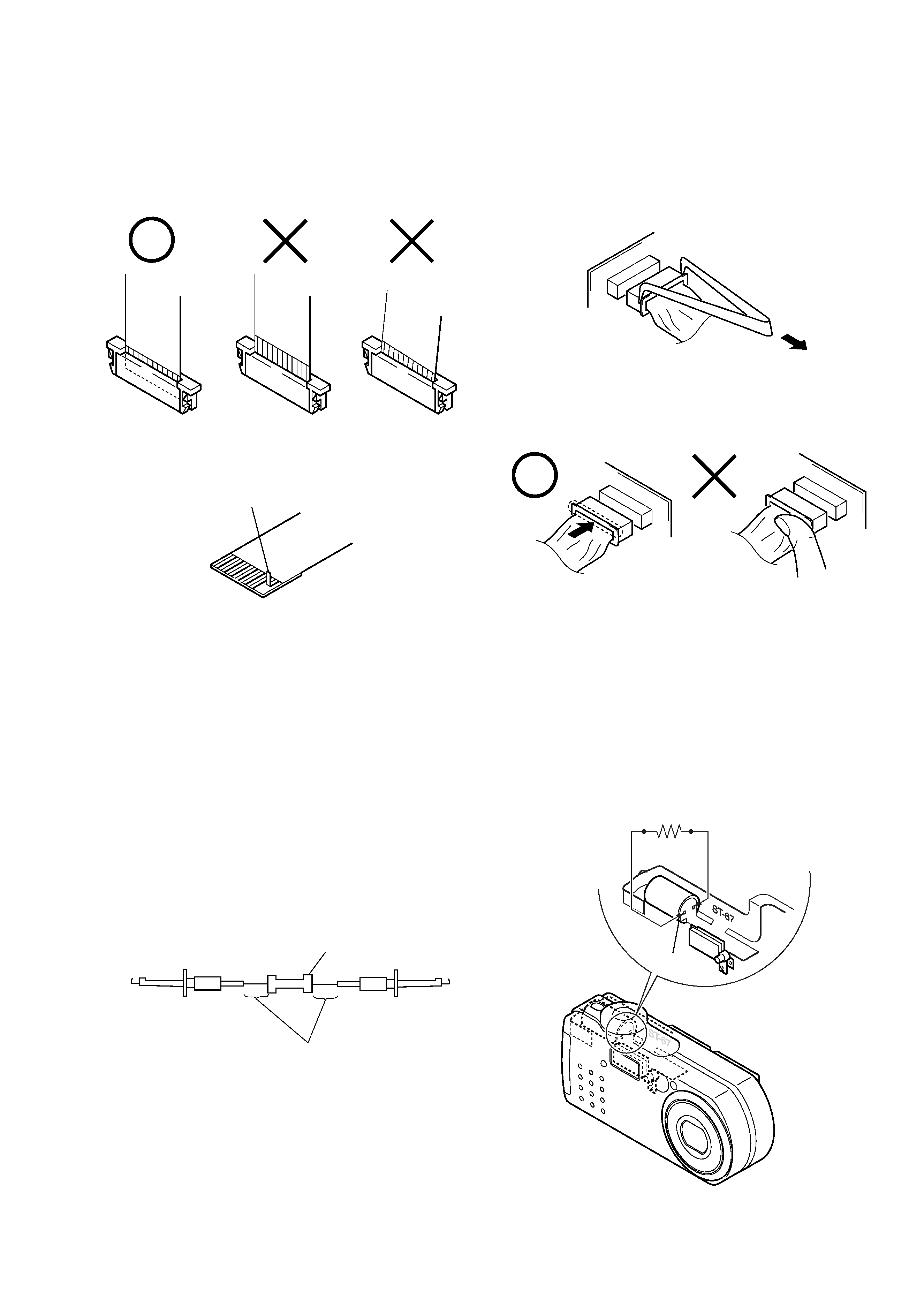
[Discharging of the ST-67 board's charging capacitor
(C008)]
The charging capacitor (C008) of the ST-67 board is charged up to
the maximum 300 V potential.
There is a danger of electric shock by this high voltage when the
battery is handled by hand. The electric shock is caused by the
charged voltage which is kept without discharging when the main
power of the unit is simply turned off. Therefore, the remaining
voltage must be discharged as described below.
Preparing the Short Jig
To preparing the short jig, a small clip is attached to each end of a
resistor of 1 k
/1 W (1-215-869-11).
Wrap insulating tape fully around the leads of the resistor to pre-
vent electrical shock.
1 k
/1 W
Wrap insulating tape.
Discharging the Capacitor
Short-circuit between the positive and the negative terminals of
charged capacitor with the short jig about 10 seconds.
SERVICE NOTE
· NOTE FOR REPAIR
Make sure that the flat cable and flexible board are not cracked of
bent at the terminal.
Do not insert the cable insufficiently nor crookedly.
Cut and remove the part of gilt
which comes off at the point.
(Be careful or some
pieces of gilt may be left inside)
When remove a connector, don't pull at wire of connector.
It is possible that a wire is snapped.
When installing a connector, don't press down at wire of connector.
It is possible that a wire is snapped.
R:1 k
/1 W
(Part code:
1-215-869-11)
Capacitor