SERVICE MANUAL
DIGITAL PHOTO PRINTER
AEP Model
UK Model
SPECIFICATIONS
DPP-MS300E
9-928-127-31
Continued on next page
2
Flexible Circuit Board Repairing
· Keep the temperature of the soldering iron around 270 °C dur-
ing repairing.
· Do not touch the soldering iron on the same conductor of the
circuit board (within 3 times).
· Be careful not to apply force on the conductor when soldering
or unsoldering.
Notes on chip component replacement
· Never reuse a disconnected chip component.
· Notice that the minus side of a tantalum capacitor may be dam-
aged by heat.
ADVARSEL
Eksplosjonsfare ved feilaktig skifte av batteri.
Benytt samme batteritype eller en tilsvarende type
anbefalt av apparatfabrikanten.
Brukte batterier kasseres i henhold til fabrikantens
instruksjoner.
VARNING
Explosionsfara vid felaktigt batteribyte.
Använd samma batterityp eller en likvärdig typ som
rekommenderas av apparattillverkaren.
Kassera använt batteri enligt gällande föreskrifter.
VAROITUS
Paristo voi räjähtää, jos se on virheellisesti asennettu.
Vaihda paristo ainoastaan laitevalmistajan suosittelemaan tyyppiin.
Hävitä käytetty paristo valmistajan ohjeiden mukaisesti.
ADVARSEL!
Lithiumbatteri-Eksplosionsfare ved fejlagtig håndtering.
Udskiftning må kun ske med batteri
af samme fabrikat og type.
Levér det brugte batteri tilbage til leverandøren.
CAUTION
Danger of explosion if battery is incorrectly replaced.
Replace only with the same or equivalent type recommended by
the manufacturer.
Discard used batteries according to the manufacturer's instructions.
SAFETY-RELATED COMPONENT WARNING!!
COMPONENTS IDENTIFIED BY MARK
! OR DOTTED
LINE WITH MARK
! ON THE SCHEMATIC DIAGRAMS
AND IN THE PARTS LIST ARE CRITICAL TO SAFE
OPERATION. REPLACE THESE COMPONENTS WITH
SONY PARTS WHOSE PART NUMBERS APPEAR AS
SHOWN IN THIS MANUAL OR IN SUPPLEMENTS PUB-
LISHED BY SONY.

3
TABLE OF CONTENTS
1.
GENERAL
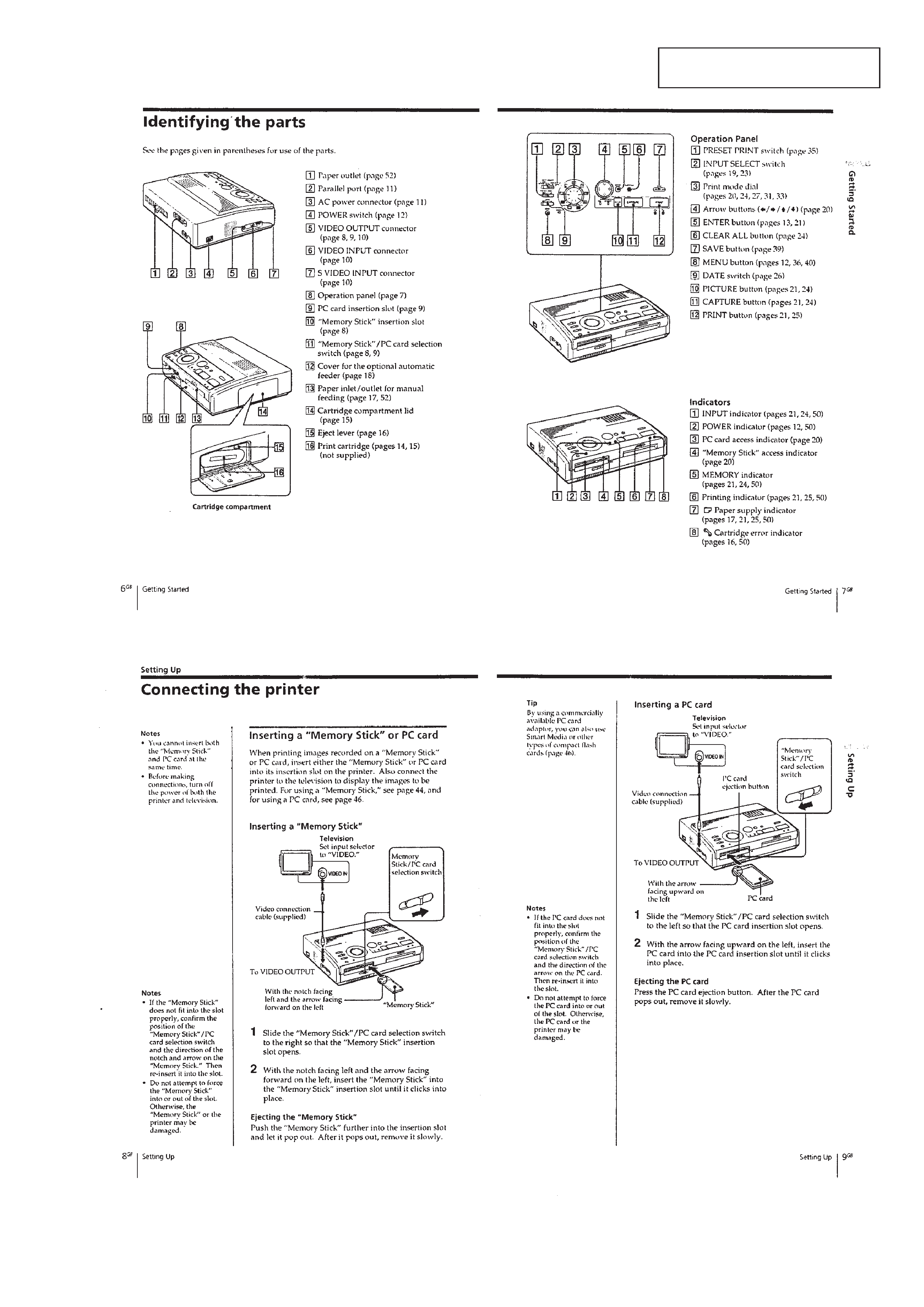
Identifying the parts ..................................................... 1-1
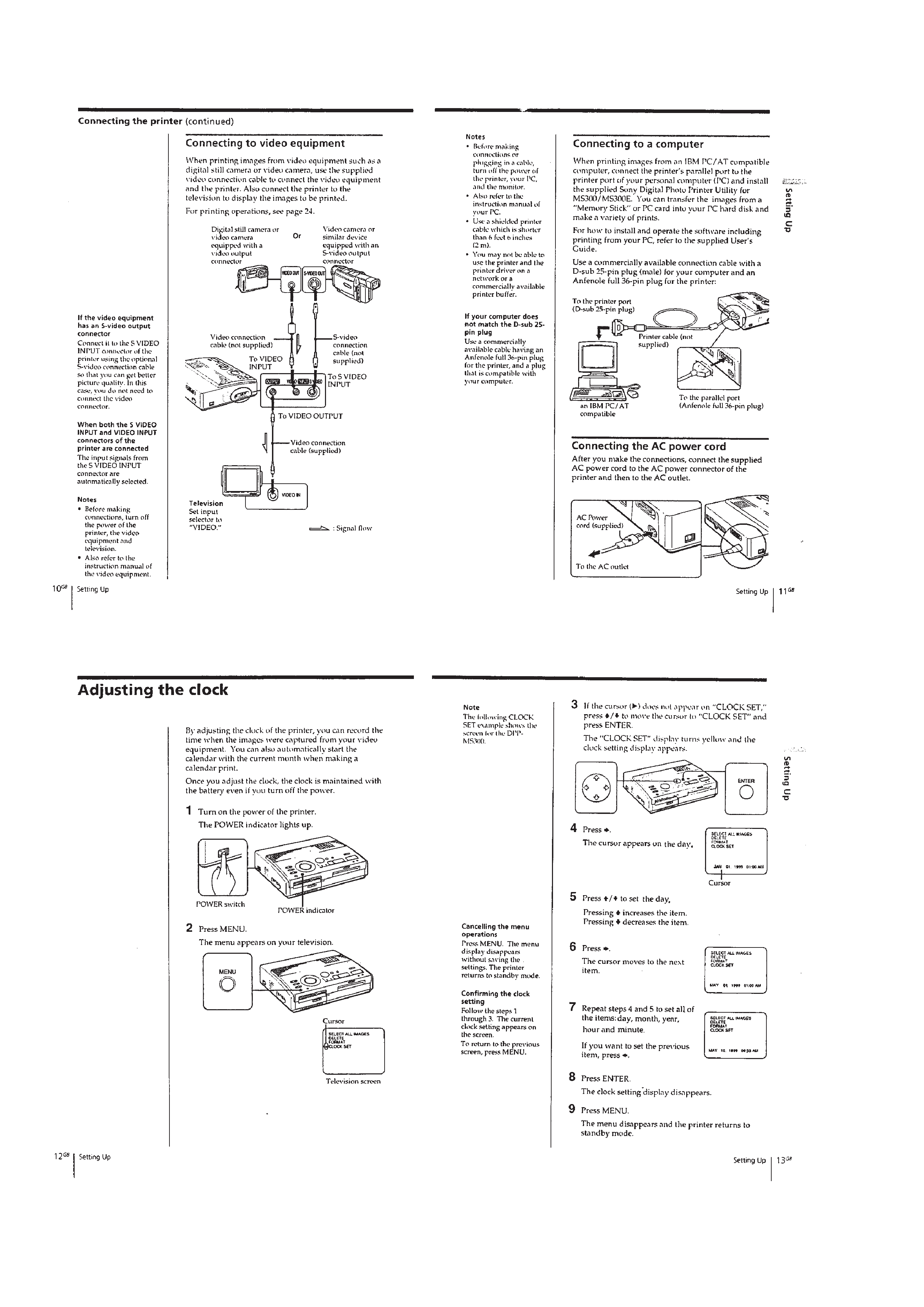
Setting Up .................................................................... 1-1
Printing ......................................................................... 1-4
Making Various Prints .................................................. 1-6
About "Memory Stick" ................................................ 1-10
About PC Cards ........................................................... 1-10
2.
DISASSEMBLY ...................................................... 2-1
3.
MECHANICAL ADJUSTMENTS .................... 3-1
4.
ELECTRICAL ADJUSTMENTS ...................... 4-1
Power Supply Block .................................................... 4-3
Video Block .................................................................. 4-4
5.
DIAGRAMS
5-1.
Block Diagram VIDEO Section ........................... 5-1
5-2.
Block Diagram MAIN Section .............................. 5-3
5-3.
Block Diagram CENTRONICS Section .............. 5-5
5-4.
Block Diagram
PC CARD/MEMORY STICK Section ................. 5-7
5-5.
Block Diagram
HEAD/SENSOR/MOTOR/
POWER SUPPLY Section ........................................ 5-9
5-6.
Frame Schematic Diagram .......................................... 5-11
5-7.
Notes for Printed Wiring Board and
Schematic Diagram ...................................................... 5-13
5-8.
Printed Wiring Board VS-40 Board ..................... 5-15
5-9.
Schematic Diagram VS-40 Board ......................... 5-16
5-10. Printed Wiring Board VI-40 Board ....................... 5-17
5-11. Schematic Diagram VI-40 Board .......................... 5-19
5-12. Printed Wiring Board DK-40 Board ..................... 5-23
5-13. Schematic Diagram DK-40 Board (1/3) ............... 5-25
5-14. Schematic Diagram DK-40 Board (2/3) ............... 5-28
5-15. Schematic Diagram DK-40 Board (3/3) ............... 5-31
5-16. Printed Wiring Board MP-40 Board ..................... 5-33
5-17. Schematic Diagram MP-40 Board ........................ 5-35
5-18. Printed Wiring Boards FE-40/JK-40 Boards ....... 5-39
5-19. Schematic Diagram FE-40/JK-40 Boards ............. 5-41
5-20. Printed Wiring Board SW-40 Board ..................... 5-43
5-21. Schematic Diagram SW-40 Board ........................ 5-45
5-22. Printed Wiring Boards
HP-40/JD-40/MD-40/RD-40 Boards .................... 5-47
5-23. Schematic Diagram
HP-40/JD-40/MD-40/RD-40 Boards .................... 5-49
5-24. IC Pin Function Description ........................................ 5-59
6.
EXPLODED VIEWS ............................................. 6-1
7.
ELECTRICAL PARTS LIST ............................ 7-1
1-1
SECTION 1
GENERAL
This section is extracted from in-
struction manual (3-866-753-11).
1-2