SERVICE MANUAL
Sony Corporation
Personal Audio Company
Published by Sony Engineering Corporation
US Model
Canadian Model
PORTABLE CD PLAYER
9-877-798-01
2004D1679-1
© 2004.04
Ver 1.0 2004.04
SPECIFICATIONS
D-NS707F
Manufactured under license from Dolby
Laboratories Licensing Corporation.
CD player
System
Compact disc digital audio system
Laser diode properties
Material: GaAlAs
Wavelength:
= 770 - 800 nm
Emission duration: Continuous
Laser output: Less than 44.6
µW
(This output is the value measured at a distance
of 200 mm from the objective lens surface on the
optical pick-up block with 7 mm aperture.)
D-A conversion
1-bit quartz time-axis control
Frequency response
20 - 20 000 Hz +1
2 dB (measured by JEITA)
Output (at 4.5 V input level)
Headphones (stereo minijack)
Approx. 5 mW + Approx. 5 mW at 16
Operating temperature
5
°C - 35°C (41°F - 95°F)
Dimensions (w/h/d) (excluding projecting parts
and controls)
Approx. 136
30.5 136 mm (53/
8
11/
4
53/
8 in.)
Mass (excluding accessories)
Approx. 276 g (9.8 oz.)
Radio
Frequency range
· 9 kHz step:
TV: 2 - 13 ch
WB (weather band): 1 - 7 ch
FM: 87.5 - 108.0 MHz
AM: 531 - 1 710 kHz
· 10 kHz step:
TV: 2 - 13 ch
WB (weather band): 1 - 7 ch
FM: 87.5 - 108.0 MHz
AM: 530 - 1 710 kHz
Antenna
FM: Headphones/earphones cord antenna
AM: Built-in ferrite bar antenna
General
Power requirements
· LR6 (size AA) batteries: 1.5 V DC
2
· AC power adaptor (DC IN 4.5 V jack):
120 V, 60 Hz
x
x
x
x
x
Supplied accessories
Design and specifications are subject to change
without notice.
·
·
·
·
Headphones
CD-ROM (SonicStage)
Operating Instructions
SonicStage Installation/Operating Guide
Model Name Using Similar Mechanism
D-NE10
CD Mechanism Type
CDM-3325ERV2
Optical Pick-up Name
DAX-25EV
2
D-NS707F
TABLE OF CONTENTS
1.
SERVICE POSITION .......................................... 3
2.
GENERAL ............................................................ 5
3.
DISASSEMBLY
3-1.
Upper (Lid) Section .........................................................
6
3-2.
Cabinet (Middle) Section ................................................
7
3-3.
MAIN PWB Assy ............................................................
7
3-4.
MAIN Board, CD Mechanism Deck
(CDM-3325ERV2) ..........................................................
8
3-5.
Turn Table Motor Assy (M901), Sled Motor Assy (M902),
Optical Pick-up (DAX-25EV) .........................................
8
4.
ELECTRICAL CHECKING ................................ 9
5.
DIAGRAMS
5-1.
Block Diagram MAIN Section (1/2) ......................... 12
Block Diagram MAIN Section (2/2) ......................... 13
Block Diagram TUNER Section ............................... 14
Block Diagram POWER Section ............................... 15
5-2.
Printed Wiring Board MAIN Board (Side A) ............ 16
5-3.
Printed Wiring Board MAIN Board (Side B) ............ 17
5-4.
Schematic Diagrams MAIN Board (1/5) ................... 18
5-5.
Schematic Diagrams MAIN Board (2/5) ................... 19
5-6.
Schematic Diagrams MAIN Board (3/5) ................... 20
5-7.
Schematic Diagrams MAIN Board (4/5) ................... 21
5-8.
Schematic Diagrams MAIN Board (5/5) ................... 22
5-9.
IC Pin Function Descriptions .......................................... 27
6.
EXPLODED VIEWS
6-1.
Cabinet Upper .................................................................. 34
6-2.
Cabinet Lower ................................................................. 35
6-3.
Strap Front ....................................................................... 36
6-4.
MAIN PWB Assy ............................................................ 37
6-5.
CD Mechanism Deck Section (CDM-3325ERV2) .......... 38
7.
ELECTRICAL PARTS LIST ............................... 39
Unleaded solder
Boards requiring use of unleaded solder are printed with the lead-
free mark (LF) indicating the solder contains no lead.
(Caution: Some printed circuit boards may not come printed with
the lead free mark due to their particular size.)
: LEAD FREE MARK
Unleaded solder has the following characteristics.
·
Unleaded solder melts at a temperature about 40
°C higher than
ordinary solder.
Ordinary soldering irons can be used but the iron tip has to be
applied to the solder joint for a slightly longer time.
Soldering irons using a temperature regulator should be set to
about 350
°C.
Caution: The printed pattern (copper foil) may peel away if the
heated tip is applied for too long, so be careful!
·
Strong viscosity
Unleaded solder is more viscous (sticky, less prone to flow)
than ordinary solder so use caution not to let solder bridges
occur such as on IC pins, etc.
·
Usable with ordinary solder
It is best to use only unleaded solder but unleaded solder may
also be added to ordinary solder.
This appliance is classified as a CLASS 1 LASER product. The
CLASS 1 LASER PRODUCT MARKING is located on the rear
exterior.
Flexible Circuit Board Repairing
·Keep the temperature of soldering iron around 270°C
during repairing.
· Do not touch the soldering iron on the same conductor of the
circuit board (within 3 times).
· Be careful not to apply force on the conductor when soldering
or unsoldering.
Notes on chip component replacement
·Never reuse a disconnected chip component.
· Notice that the minus side of a tantalum capacitor may be
damaged by heat.
CAUTION
Use of controls or adjustments or performance of procedures
other than those specified herein may result in hazardous radiation
exposure.
On AC power adaptor
·Use only the AC power adaptor supplied or
recommended in "Accessories (supplied/
optional)." Do not use any other AC power
adaptor. It may cause a malfunction.
Polarity of the plug
3
D-NS707F
SECTION 1
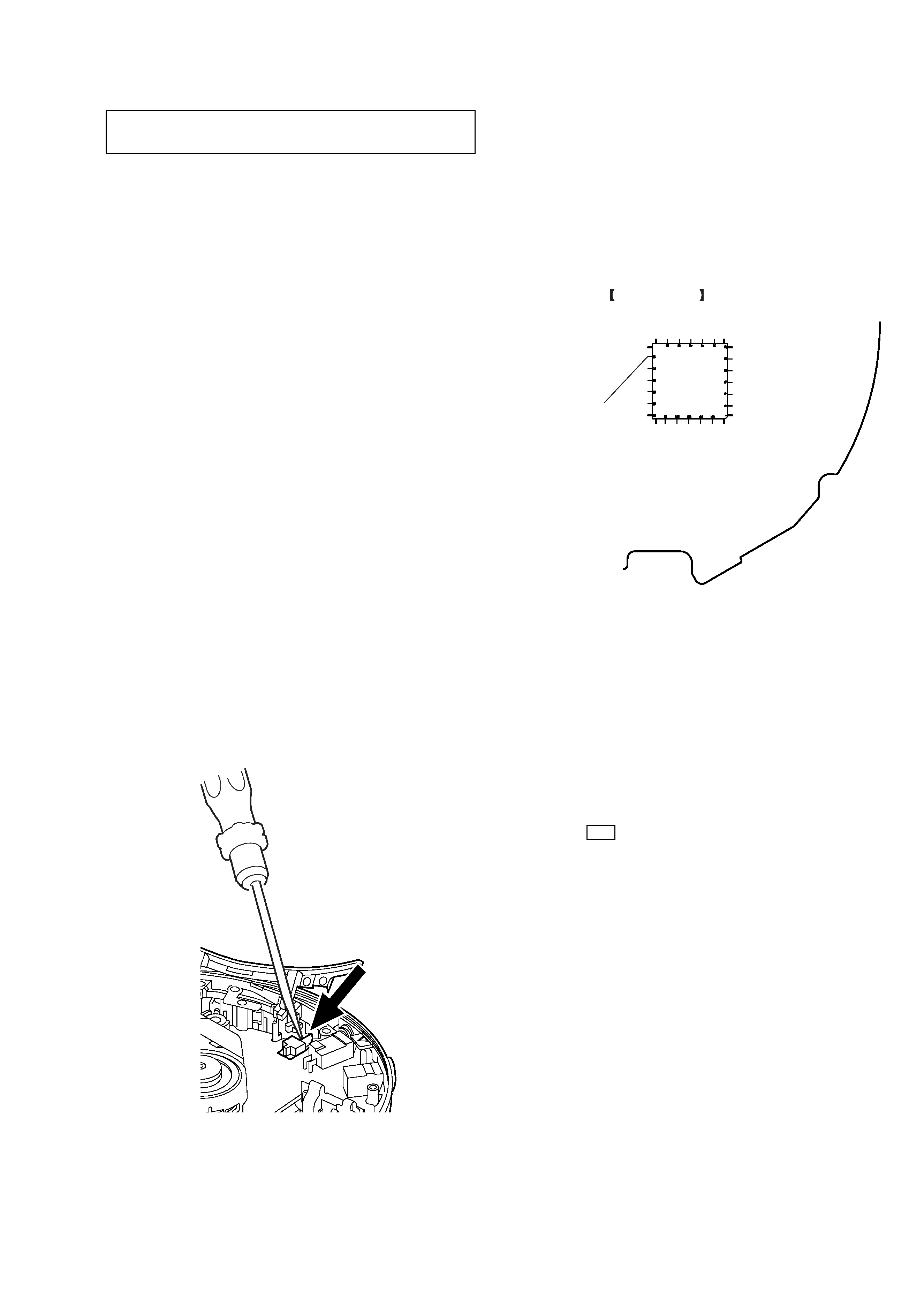
SERVICING NOTE
Fig. 1 Method to push the S820
LASER DIODE AND FOCUS SEARCH OPERATION
CHECK
During normal operation of the equipment, emission of the laser
diode is prohibited unless the upper lid is closed while turning ON
the S820.
The following checking method for the laser diode is operable.
· Method:
Emission of the laser diode is visually checked.
1. Remove the upper lid.
2. With a disc not set, turn on the S820 with a screwdriver having
a thin tip as shown in Fig.1.
3. Press the u button.
4. Observing the objective lens, check that the laser diode emits
light.
When the laser diode does not emit light, automatic power con-
trol circuit or optical pickup is faulty.
In this operation, the objective lens will move up and down 4
times along with inward motion for the focus search.
NOTES ON HANDLING THE OPTICAL PICK-UP
BLOCK OR BASE UNIT
The laser diode in the optical pick-up block may suffer electrostatic
breakdown because of the potential difference generated by the
charged electrostatic load, etc. on clothing and the human body.
During repair, pay attention to electrostatic breakdown and also use
the procedure in the printed matter which is included in the repair
parts.
The flexible board is easily damaged and should be handled with
care.
NOTES ON LASER DIODE EMISSION CHECK
The laser beam on this model is concentrated so as to be focused on
the disc reflective surface by the objective lens in the optical pick-
up block. Therefore, when checking the laser diode emission, ob-
serve from more than 30 cm away from the objective lens.
SAFETY-RELATED COMPONENT WARNING!!
COMPONENTS IDENTIFIED BY MARK 0 OR DOTTED LINE WITH
MARK 0 ON THE SCHEMATIC DIAGRAMS AND IN THE PARTS
LIST ARE CRITICAL TO SAFE OPERATION. REPLACE THESE
COMPONENTS WITH SONY PARTS WHOSE PART NUMBERS
APPEAR AS SHOWN IN THIS MANUAL OR IN SUPPLEMENTS
PUBLISHED BY SONY.
ATTENTION AU COMPOSANT AYANT RAPPORT
À LA SÉCURITÉ!
LES COMPOSANTS IDENTIFÉS PAR UNE MARQUE 0 SUR LES
DIAGRAMMES SCHÉMATIQUES ET LA LISTE DES PIÈCES SONT
CRITIQUES POUR LA SÉCURITÉ DE FONCTIONNEMENT. NE
REMPLACER CES COMPOSANTS QUE PAR DES PIÈSES SONY
DONT LES NUMÉROS SONT DONNÉS DANS CE MANUEL OU
DANS LES SUPPÉMENTS PUBLIÉS PAR SONY.
BEFORE REPLACING THE OPTICAL PICK-UP BLOCK
Please be sure to check thoroughly the parameters as par the "Opti-
cal Pick-Up Block Checking Procedures" (Part No.: 9-960-027-11)
issued separately before replacing the optical pick-up block.
Note and specifications required to check are given below.
· FOK output: IC601 yg pin
When checking FOK, remove the lead wire to disc motor.
· RF signal P-to-P value: 0.45 to 0.65 Vp-p
IC601 FOK output ygpin
1
30
31
60
61
90
91
120
MAIN BOARD (SIDE B)
4
D-NS707F
2. Operation when the Service Mode is set.
When the Service Mode becomes active, following messages are
displayed onthe remote control LCD.
1) Turn off the power.
2) Open the solder land TAP824 (TEST) on the MAIN board.
Note :
The solder should be removed clean.
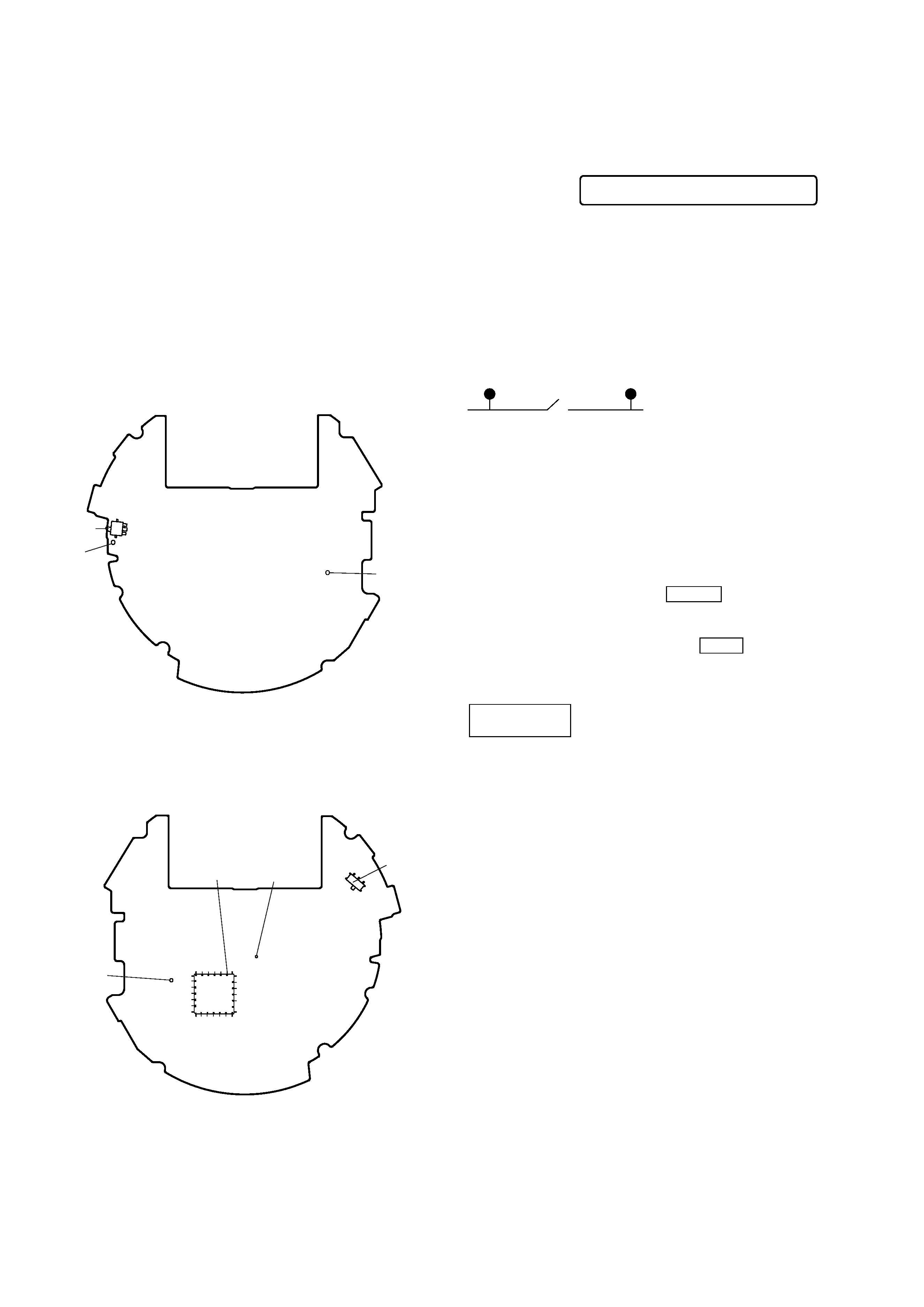
3. How to set the Tuner Service Mode.
To set the tuner Service Mode, the following method is available.
1) Confirm the set is not powered on.
2) Connect a external switch between TJ80 (Tu Test) and TJ81
(Gnd).
SERVICE MODE
The following confirmation can be performed when the Service
Mode is set.
1. How to set the CD Service Mode.
To set the Service Mode, the following method is available.
1) Confirm the set is not powered on.
2) Confirm the following settings.
OPEN/CLOSE detect switch (S820) ................. OFF
Solder Land (TAP833) ...................................... OPEN
[HOLD] switch (S803) ........................................ OFF
3) Short the solder land TAP824 (TEST) on the MAIN board.
4) Turn on the main power.
S820
TAP824
TAP833
MAIN BOARD(SIDE A)
IC601yg
S803
TP746
TP538
MAIN BOARD(SIDE B)
VS010B:
Microcomputer
version display
3) Slide the switch to connect TJ80 and TJ81 to be shorted.
4) Short the solder land TAP824 (Test).
5) Turn on the main power.
4. Operation when Tuner Service Mode is set.
When the tuner Service Mode becomes active, following the below
procedure.
1) CD microcomputer version display VS010B .
2) Press play key.
3) Display panel show all segments turn on.
4) Then show DTS microcontroller version: 00008
5) Slide the switch to oposite direction to open the connection of
TJ80(Tu test) and TJ81(Gnd).
6) Tuner mode turned on and display panel show :
FM
87.50 MHz
7) After checking complete, turn of the power.
8) Open solder land TAP824 (Test) and remove the external switch.
Note :
The solder should be removed clean.
TJ81
(Gnd)
TJ80
(TU Test)
5
D-NS707F
SECTION 2
GENERAL
This section is extracted
from instruction manual.
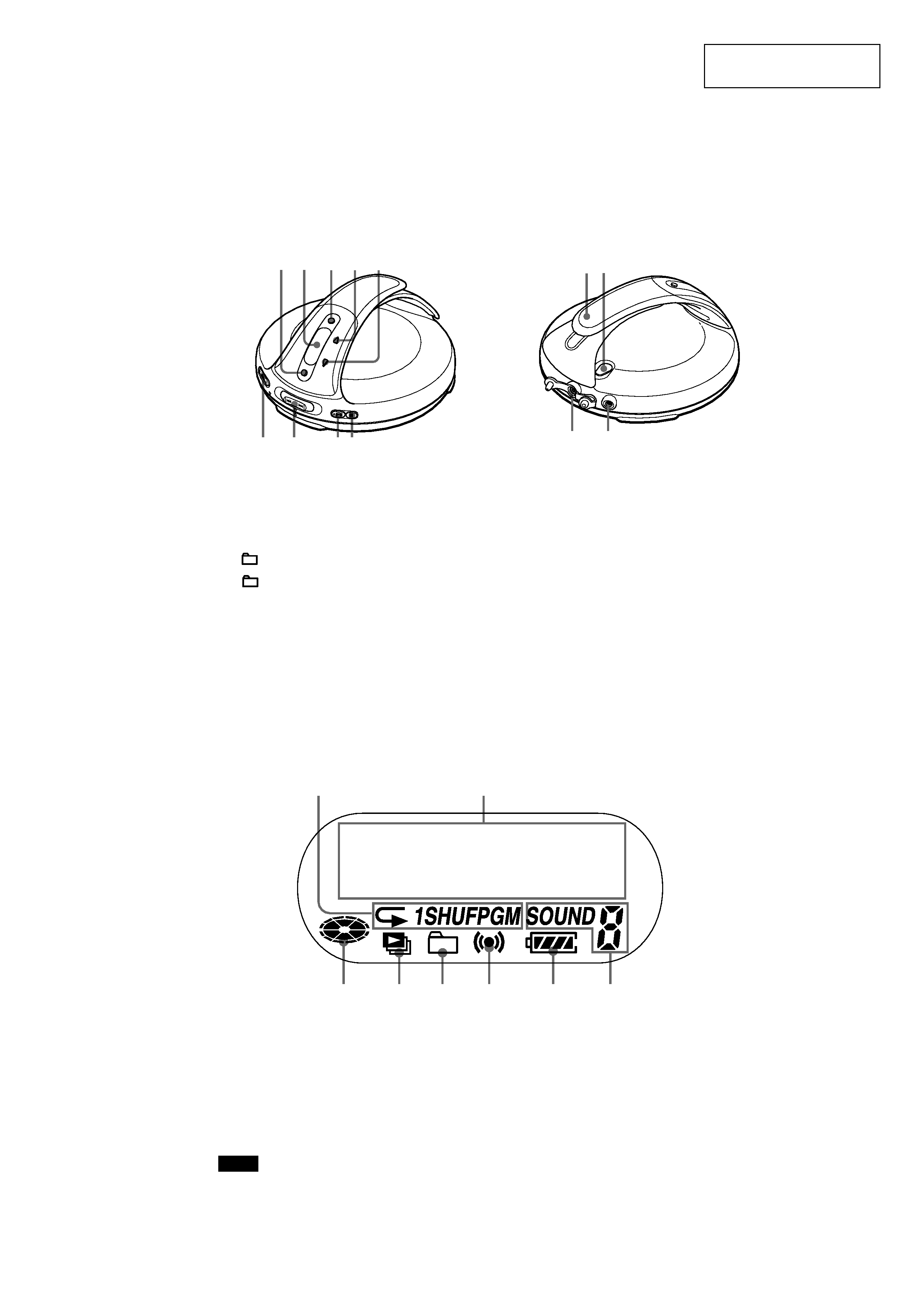
Guide to parts and Controls
1
2
u
3
x
4
5
6
7
8
* This button has a tactile dot.
9
0
qa
qs i
H
h
RADIO ON/BAND·MEMORY button
Display
DISPLAY/MENU button
(group)
·TUNE
button
VOL (volume) +*/ buttons
(group)
·TUNE
button
H
h
/PRESET ,
/PRESET + lever
.
>
(play/pause)*/ENTER button
(stop)·RADIO OFF button
Hand strap
HOLD switch
(headphones) jack
DC IN 4.5 V (external power input) jack
qd
67
89
3
2
14 5
0
qs
qd
qa
Display
qf
Play mode indicator
Character information display
Disc indicator
Play list indicator
Group indicator
Timer indicator
Battery indicator
SOUND indicator
Note
You can invert the characters on the display.
qg
qh
qj
qk
ql
w;
wa
qh
qf
qg
qj
qk
ql
w;
wa