PORTABLE CD PLAYER
US Model
Canadian Model
D-NE005
AEP Model
D-NE004/NE005/NE006
UK Model
D-NE004
E Model
D-NE005/NE0050/NE006
Australian Model
D-NE005
Tourist Model
D-NE006
SPECIFICATIONS
D-NE004/NE005/
NE0050/NE006
Ver. 1.3 2005.12
Model Name Using Similar Mechanism
NEW
CD Mechanism Type
CDM-3525A/3525AJ
Optical Pick-up Name
DAX-25E
9-879-861-04
2005L02-1
© 2005.12
Sony Corporation
Personal Audio Division
Published by Sony Engineering Corporation
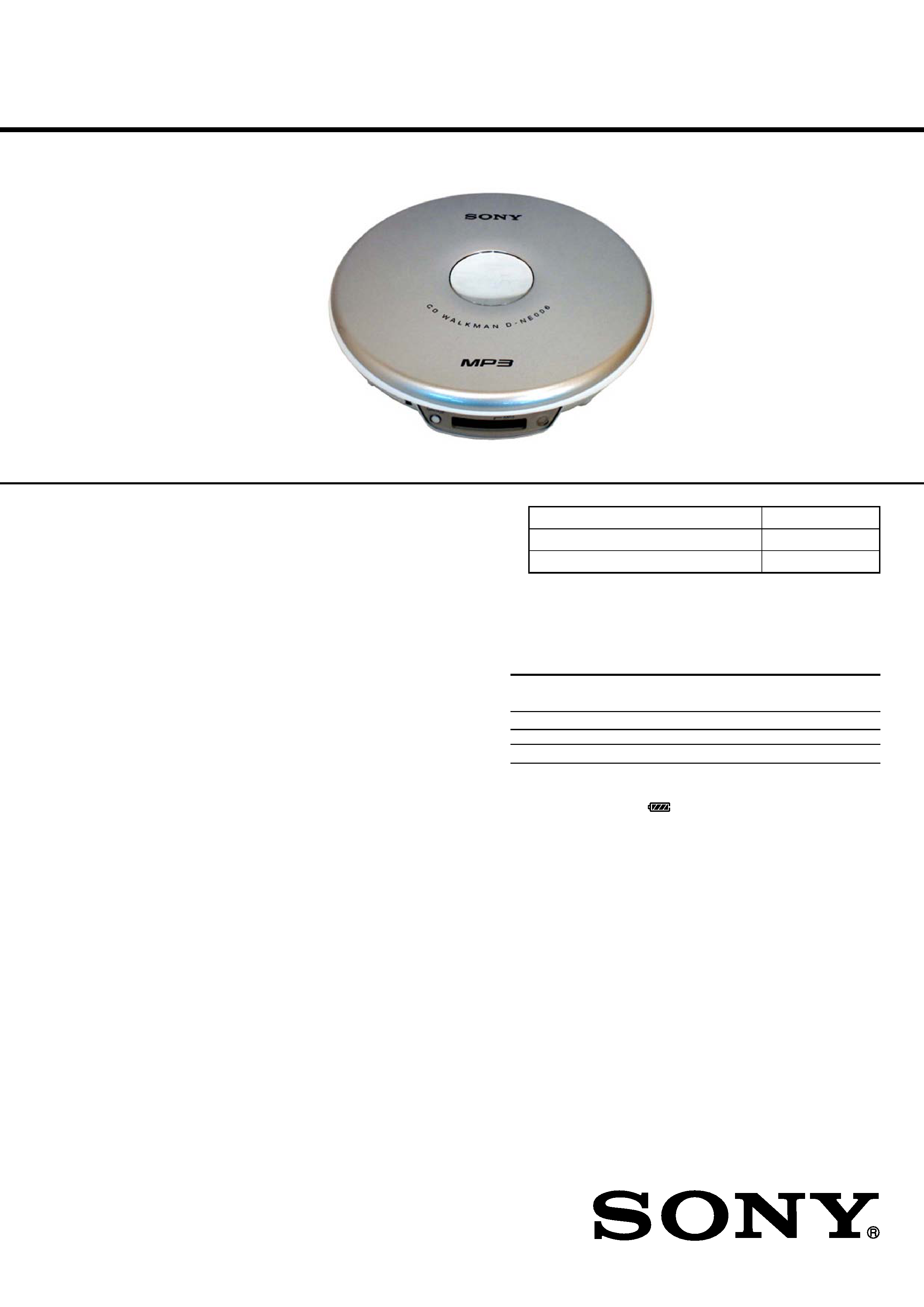
SERVICE MANUAL
Photo: D-NE006
System
Compact disc digital audio system
Laser diode properties
Emission duration: Continuous
Laser output: Less than 44.6
µW (This output is the value measured at a
distance of 200 mm from the objective lens surface on the optical pick-up
block with 7 mm aperture.)
Power requirements
· Two LR6 (size AA) batteries: 1.5 V DC
× 2
· AC power adaptor (DC IN 4.5 V jack):
220 V, 50 Hz (NE005: EE,EU8/NE006: EU8, EE, E18)
120 V, 60 Hz (C&SA, MX)
Dimensions (w/h/d) (without projecting parts and controls)
Approx. 139.8
× 28.8 × 139.8 mm
Mass (excluding accessories)
Approx. 200 g
Operating temperature
5
°C - 35°C
MPEG Layer-3 audio coding technology and patents licensed from
Fraunhofer IIS and Thomson.
Design and specifications are subject to change without notice.
Supplied accessories
AC power adaptor (1)
(NE005: EE, EU8/NE0050: C&SA, MX/NE006: EU8, EE, E18)
Headphones (1)
Remote control (1) (supplied with D-NE006 only)
Battery life* (approx. hours)
(When the CD player is used on a flat and stable place.)
Playing time varies depending on how the CD player is used.
When using two Sony alkaline batteries LR6 (SG)
(produced in Japan)
G-PROTECTION
G-on
G-off
Audio CD
16
11
MP3 CD (Recorded at 128 kbps)
23
23
* Measured value by the standard of JEITA (Japan Electronics and
Information Technology Industries Association).
· The indicator sections of
roughly show the remaining battery
power. One section does not always indicate one-fourth of the battery
power.
2
D-NE004/NE005/NE0050/NE006
Notes on chip component replacement
· Never reuse a disconnected chip component.
· Notice that the minus side of a tantalum capacitor may be
damaged by heat.
Flexible Circuit Board Repairing
· Keep the temperature of the soldering iron around 270 °C
during repairing.
· Do not touch the soldering iron on the same conductor of the
circuit board (within 3 times).
· Be careful not to apply force on the conductor when soldering
or unsoldering.
CAUTION
Use of controls or adjustments or performance of procedures
other than those specified herein may result in hazardous radiation
exposure.
TABLE OF CONTENTS
1.
SERVICING NOTES ................................................ 3
2.
GENERAL ................................................................... 3
3.
DISASSEMBLY
3-1.
Disassembly Flow ...........................................................
4
3-2.
Upper Lid Assy, Cabinet (Middle) Assy,
Cabinet (Lower) Assy ......................................................
4
3-3.
Optical Pick-Up (CDM-3525A) ......................................
5
3-4.
JACK Board, MAIN Board .............................................
5
3-5.
LPF Board .......................................................................
6
4.
TEST MODE ............................................................... 7
5.
ELECTRICAL ADJUSTMENT ............................. 7
6.
DIAGRAMS ................................................................. 8
6-1.
Block Diagram ................................................................
9
6-2.
Printed Wiring Board
MAIN Board (Side A), LPF Board (Side A) ............. 10
6-3.
Printed Wiring Board
MAIN Board (Side B), LPF Board (Side B),
JACK Board ................................................................. 11
6-4.
Schematic Diagram MAIN Board (1/2),
JACK Board (1/2) ........................................................ 12
6-5.
Schematic Diagram MAIN Board (2/2), LPF Board,
JACK Board (2/2) ........................................................ 13
6-6.
IC Pin Function Description ............................................ 15
7.
EXPLODED VIEWS
7-1.
Upper Lid, Cabinet (Middle) Section .............................. 17
7-2.
Cabinet (Lower) Section ................................................. 18
8.
ELECTRICAL PARTS LIST .................................. 19
UNLEADED SOLDER
Boards requiring use of unleaded solder are printed with the lead-
free mark (LF) indicating the solder contains no lead.
(Caution: Some printed circuit boards may not come printed with
the lead free mark due to their particular size)
: LEAD FREE MARK
Unleaded solder has the following characteristics.
· Unleaded solder melts at a temperature about 40 °C higher
than ordinary solder.
Ordinary soldering irons can be used but the iron tip has to be
applied to the solder joint for a slightly longer time.
Soldering irons using a temperature regulator should be set to
about 350
°C.
Caution: The printed pattern (copper foil) may peel away if
the heated tip is applied for too long, so be careful!
· Strong viscosity
Unleaded solder is more viscou-s (sticky, less prone to flow)
than ordinary solder so use caution not to let solder bridges
occur such as on IC pins, etc.
· Usable with ordinary solder
It is best to use only unleaded solder but unleaded solder may
also be added to ordinary solder.
SAFETY-RELATED COMPONENT WARNING!!
COMPONENTS IDENTIFIED BY MARK
! OR DOTTED LINE WITH
MARK
!ON THE SCHEMATIC DIAGRAMS AND IN THE PARTS
LIST ARE CRITICAL TO SAFE OPERATION.
REPLACE THESE COMPONENTS WITH SONY PARTS WHOSE
PART NUMBERS APPEAR AS SHOWN IN THIS MANUAL OR IN
SUPPLEMENTS PUBLISHED BY SONY.
ATTENTION AU COMPOSANT AYANT RAPPORT
À LA SÉCURITÉ!
LES COMPOSANTS IDENTIFÉS PAR UNE MARQUE 0 SUR
LES DIAGRAMMES SCHÉMATIQUES ET LA LISTE DES
PIÈCES SONT CRITIQUES POUR LA SÉCURITÉ DE
FONCTIONNEMENT. NE REMPLACER CES COMPOSANTS
QUE PAR DES PIÈSES SONY DONT LES NUMÉROS SONT
DONNÉS DANS CE MANUEL OU DANS LES SUPPÉMENTS
PUBLIÉS PAR SONY.
3
D-NE004/NE005/NE0050/NE006
SECTION 1
SERVICING NOTES
NOTES ON HANDLING THE OPTICAL PICK-UP
BLOCK OR BASE UNIT
The laser diode in the optical pick-up block may suffer electrostatic
break-down because of the potential difference generated by the
charged electrostatic load, etc. on clothing and the human body.
During repair, pay attention to electrostatic break-down and also
use the procedure in the printed matter which is included in the
repair parts.
The flexible board is easily damaged and should be handled with
care.
NOTES ON LASER DIODE EMISSION CHECK
The laser beam on this model is concentrated so as to be focused on
the disc reflective surface by the objective lens in the optical pick-
up block. Therefore, when checking the laser diode emission,
observe from more than 30 cm away from the objective lens.
LASER DIODE AND FOCUS SEARCH OPERATION
CHECK
During normal operation of the equipment, emission of the laser
diode is prohibited unless the upper lid is closed while turning ON
the S811. (push switch type)
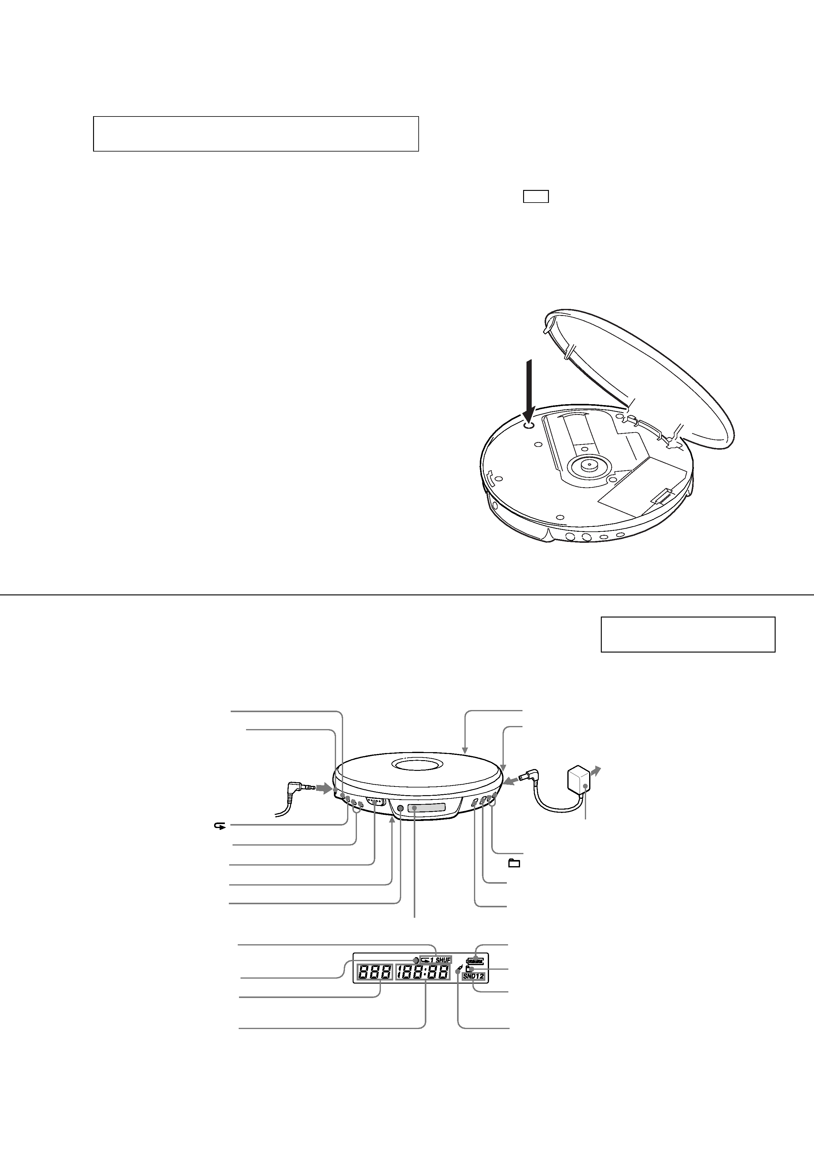
The following checking method for the laser diode is operable.
Fig. 1 Method to push the S811
S811
SECTION 2
GENERAL
This section is extracted from
instruction manual.
LOCATING THE CONTROLS
Headphones
P MODE/
VOL +*/
SOUND/AVLS
LINE OUT (European and Tourist model only)
DC IN 4.5V
to an AC outlet
(group)/+
*(play/pause)
·
AC power adaptor
Display
./>
i
(headhpones) jack
OPEN
HOLD (rear)
GROUP
Play mode
MP3 indicator
Track number
Playing time
u
(stop)
Remaining battery power
Group indicator
Sound mode
Bookmark
* The button has a tactile dot.
x
· Method:
Emission of the laser diode is visually checked.
1. Open the upper lid.
2. With a disc not set, turn on the S811 with a screwdriver having
a thin tip as shown in Fig.1.
3. Press the u button.
4. Observing the objective lens, check that the laser diode emits
light.
When the laser diode does not emit light, automatic power
control circuit or optical pick-up is faulty.
In this operation, the objective lens will move up and down 2
times along with inward motion for the focus search.
Ver. 1.2
4
D-NE004/NE005/NE0050/NE006
SECTION 3
DISASSEMBLY
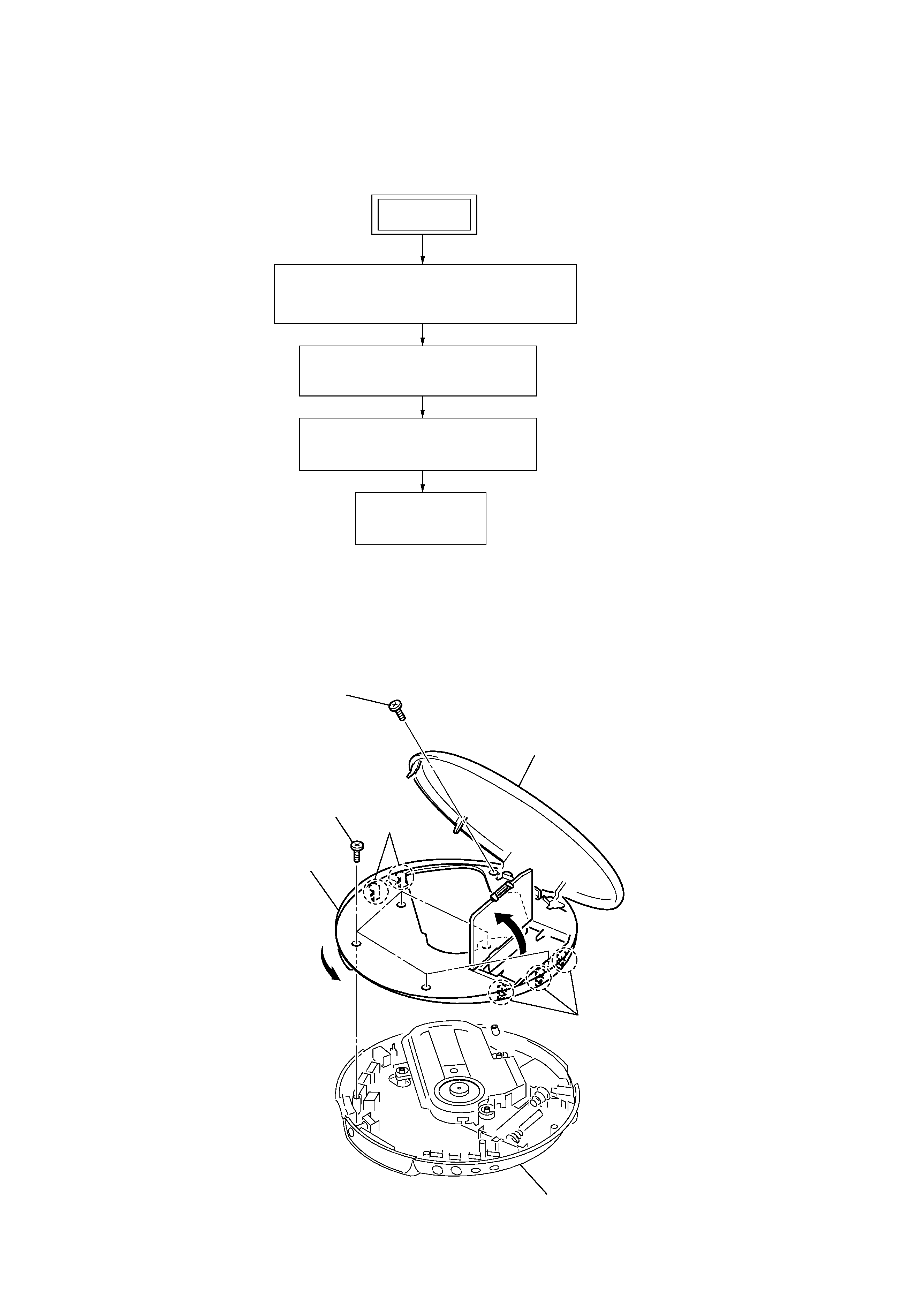
· This set can be disassembled in the order shown below.
3-1. DISASSEMBLY FLOW
3-2. UPPER LID ASSY, CABINET (MIDDLE) ASSY, CABINET (LOWER) ASSY
Note: Follow the disassembly procedure in the numerical order given.
3-2. UPPER LID ASSY, CABINET (MIDDLE) ASSY,
CABINET (LOWER) ASSY
(Page 4)
3-3. OPTICAL PICK-UP (CDM-3525A)
(Page 5)
3-4. JACK BOARD, MAIN BOARD
(Page 5)
3-5. LPF BOARD
(Page 6)
SET
4
screw
upper lid assy
cabinet (middle) assy
cabinet (lower) assy
3
five screws
2
5
two claws
6
three claws
1
OPEN
5
D-NE004/NE005/NE0050/NE006
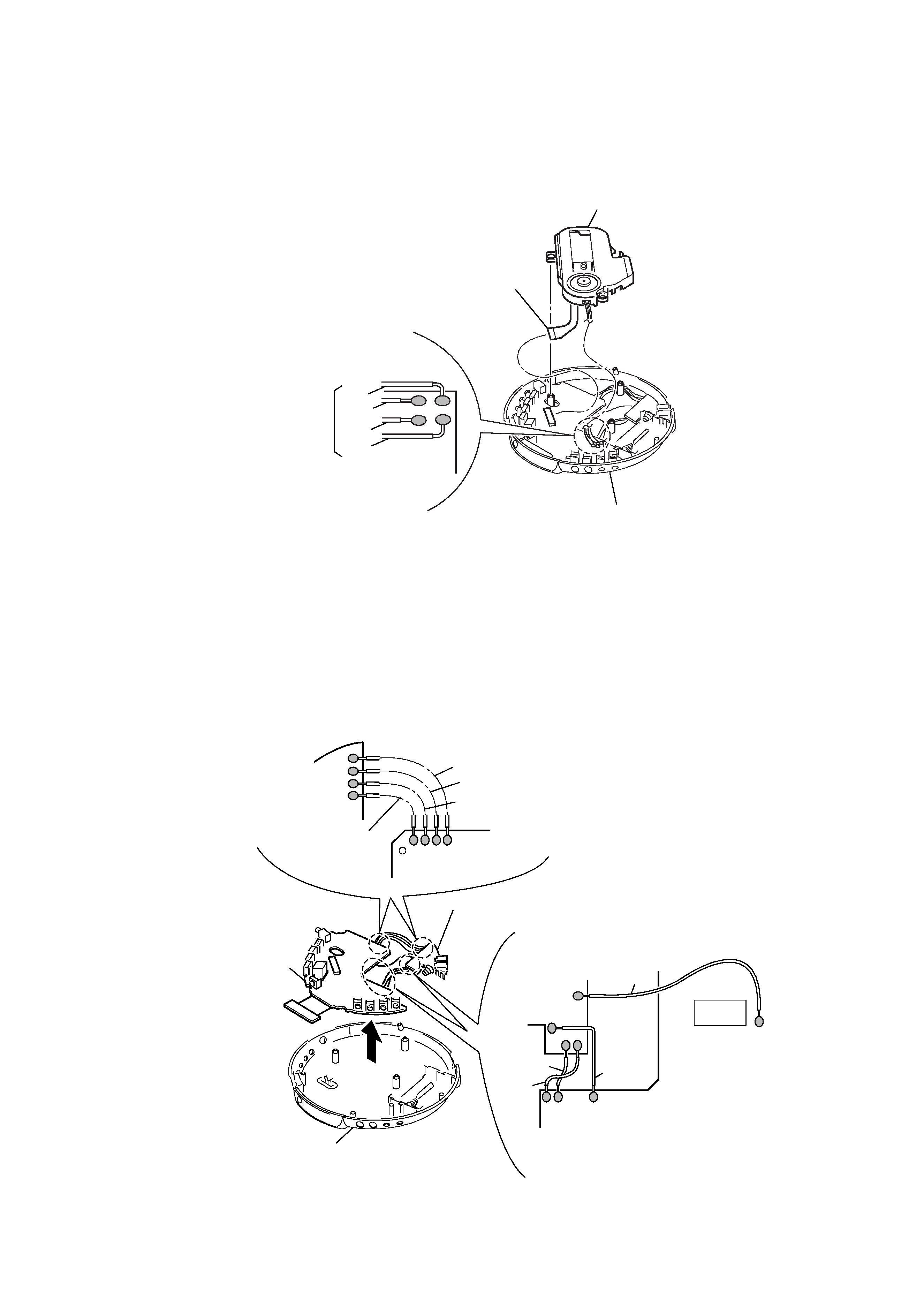
3-3. OPTICAL PICK-UP (CDM-3525A)
cabinet (lower) assy
3
optical pick-up (CDM-3525A)
1
CN501
To/From
Optical pick-up
(CDM-3525A)
2
Unsolder four lead wires
MAIN Board (side A)
BLK
ORG
GRY
RED
3-4. JACK BOARD, MAIN BOARD
MAIN Board (side B)
MAIN Board (side B)
JACK Board
(side B)
JACK Board
(side B)
BLK
RED
WHT
BLU
IC602
1
25
26
50
TP412
SGND
BLK
RED
GRY
ORG
4
JACK board
1
5
MAIN board
cabinet (lower) assy
2
Unsolder four lead wires
3
Unsolder four lead wires (AEP, EE, EU8 only)
· Abbreviation
EE
: East European
EU8
: European model other than UK, EE
and Russian