-- 1 --
MiNi DiSC DECK
MICROFILM
MDS-M9
SPECIFICATIONS
US and foreign patents licensed from Dolby Laboratories Licensing Corpo-
ration.
US Model
Canadian Model
E Model
Tourist Model
SERVICE MANUAL
MDS-M9 is the Mini disc deck
section in DHC-MD7.
Model Name Using Similar Mechanism
MDS-302
MD Mechanism Type
MDM-2B
Base Unit Type
MBU-2
Optical Pick-up Type
KMS-210A/J-N
-- 2 --
MODEL IDENTIFICATION
-- BACK PANEL --
4-977-679-3
4-977-679-2
PARTS No.
US,Canadian model
Other model
TABLE OF CONTENTS
1. SERVICE NOTE ........................................................... 4
2. GENERAL .................................................................... 6
3. TEST MODE
3-1.
Setting the Test Mode ......................................................... 11
3-2.
Exiting the Test Mode ........................................................ 11
3-3.
Basic Operations of the Test Mode .................................... 11
3-4.
Selecting the Test Mode ..................................................... 11
3-4-1. Operating the Continuous Playback Mode .............. 11
3-4-2. Operating the Continuous Recording Mode ............ 12
3-4-3. Non-Volatile Memory Mode .................................... 12
3-5.
Functions of Other buttons ................................................. 12
3-6.
Test Mode Displays ............................................................ 13
3-7.
Meanings of Other Displays ............................................... 13
3-8.
Precautions for Use of Test Mode ...................................... 13
4. ELECTRICAL ADJUSTMENTS
4-1.
Precautions for Checking Laser Diode Emission ............... 14
4-2.
Precautions for Use of optical pickup (KMS-210A) .......... 14
4-3.
Precautions for Adjustments ............................................... 14
4-4.
Creating MO Continuously Recorded Disc ........................ 14
4-5.
Temperature Compensation Offset Adjustment ................. 15
4-6.
Laser Power Adjustment ..................................................... 15
4-7.
Traverse Adjustment ........................................................... 16
4-8.
Focus Bias Adjustment ....................................................... 17
4-9.
Error Rate Check ................................................................ 17
4-9-1. CD Error Rate Check ............................................... 17
4-9-2. MO Error Rate Check .............................................. 17
4-10. Focus Bias Check ............................................................... 17
4-11. Adjusting Points and Connecting Points ............................ 18
5. DIAGRAMS
5-1.
Circuit Boards Location ..................................................... 19
5-2.
Block Diagrams .................................................................. 20
5-3.
Printed Wiring Board -- RF Section -- ............................. 26
5-4.
Schematic Diagram -- RF Section -- ............................... 29
5-5.
Schematic Diagram -- Digital Section -- ......................... 33
5-6.
Printed Wiring Board -- Digital Section -- ...................... 37
5-7.
Printed Wiring Board -- Power Section -- ....................... 41
5-8.
Schematic Diagram -- Power Section -- .......................... 42
5-9.
Schematic Diagram -- Panel Section -- ............................ 45
5-10. Printed Wiring Board -- Panel Section -- ......................... 45
5-11. IC Block Diagrams -- Digital Section -- .......................... 48
5-12. IC Pin Functions
· IC101 RF Amplifier (CXA1981AR) ............................... 49
· IC121 Digital signal processor, digital servo processor,
EFM/ACIRC encoder/decoder (CXD2535BR) ............... 50
· IC201 System Control (M37610MD-067FP) ................. 53
· IC271 Shock-Proof Memory Controller,
ATRAC Encoder/ Decoder (CXD2536R) ....................... 56
· IC301 A/D Converter (CXD8566M) ............................... 58
· IC701 Display control, LED drive .................................. 59
6. EXPLODED VIEWS
6-1.
Front Panel Section ............................................................ 60
6-2.
Chassis Section ................................................................... 61
6-3.
Mechanism Deck Section (MDM-2B) ............................... 62
6-4.
Base Unit Section (MBU-2) ............................................... 63
7. ELECTRICAL ADJUSTMENT ................................. 64
Parts No.
-- 3 --
SAFETY CHECK-OUT
After correcting the original service problem, perform the follow-
ing safety checks before releasing the set to the customer:
Check the antenna terminals, metal trim, "metallized" knobs, screws,
and all other exposed metal parts for AC leakage. Check leakage as
described below.
LEAKAGE
The AC leakage from any exposed metal part to earth Ground and
from all exposed metal parts to any exposed metal part having a
return to chassis, must not exceed 0.5 mA (500 microampers).
Leakage current can be measured by any one of three methods.
1. A commercial leakage tester, such as the Simpson 229 or RCA
WT-540A. Follow the manufacturers' instructions to use these
instruments.
2. A battery-operated AC milliammeter. The Data Precision 245
digital multimeter is suitable for this job.
3. Measuring the voltage drop across a resistor by means of a VOM
or battery-operated AC voltmeter. The "limit" indication is 0.75
V, so analog meters must have an accurate low-voltage scale.
The Simpson 250 and Sanwa SH-63Trd are examples of a pas-
sive VOM that is suitable. Nearly all battery operated digital
multimeters that have a 2V AC range are suitable. (See Fig. A)
ATTENTION AU COMPOSANT AYANT RAPPORT
À LA SÉCURITÉ!!
LES COMPOSANTS IDENTIFIÉS PAR UNE MARQUE
!SUR
LES DIAGRAMMES SCHÉMATIQUES ET LA LISTE DES
PIÈCES SONT CRITIQUES POUR LA SÉCURITÉ DE
FONCTIONNEMENT. NE REMPLACER CES COMPOSANTS
QUE PAR DES PIÈCES SONY DONT LES NUMÉROS
SONT DONNÉS DANS CE MANUEL OU DANS LES
SUPPLÉMENTS PUBLIÉS PAR SONY.
SAFETY-RELATED COMPONENT WARNING !!
COMPONENTS IDENTIFIED BY MARK
! OR DOTTED LINE
WITH MARK
! ON THE SCHEMATIC DIAGRAMS AND IN
THE PARTS LIST ARE CRITICAL TO SAFE OPERATION.
REPLACE THESE COMPONENTS WITH SONY PARTS
WHOSE PART NUMBERS APPEAR AS SHOWN IN THIS
MANUAL OR IN SUPPLEMENTS PUBLISHED BY SONY.
CAUTION
Use of controls or adjustments or performance of
procedures other than those specified herein may result in
hazardous radiation exposure.
Notes on chip component replacement
· Never reuse a disconnected chip component.
· Notice that the minus side of a tantalum capacitor may be
damaged by heat.
Flexible Circuit Board Repairing
· Keep the temperature of soldering iron around 270°C
during repairing.
· Do not touch the soldering iron on the same conductor of the
circuit board (within 3 times).
· Be careful not to apply force on the conductor when soldering
or unsoldering.
Laser component in this product is capable of emitting radiation
exceeding the limit for Class 1.
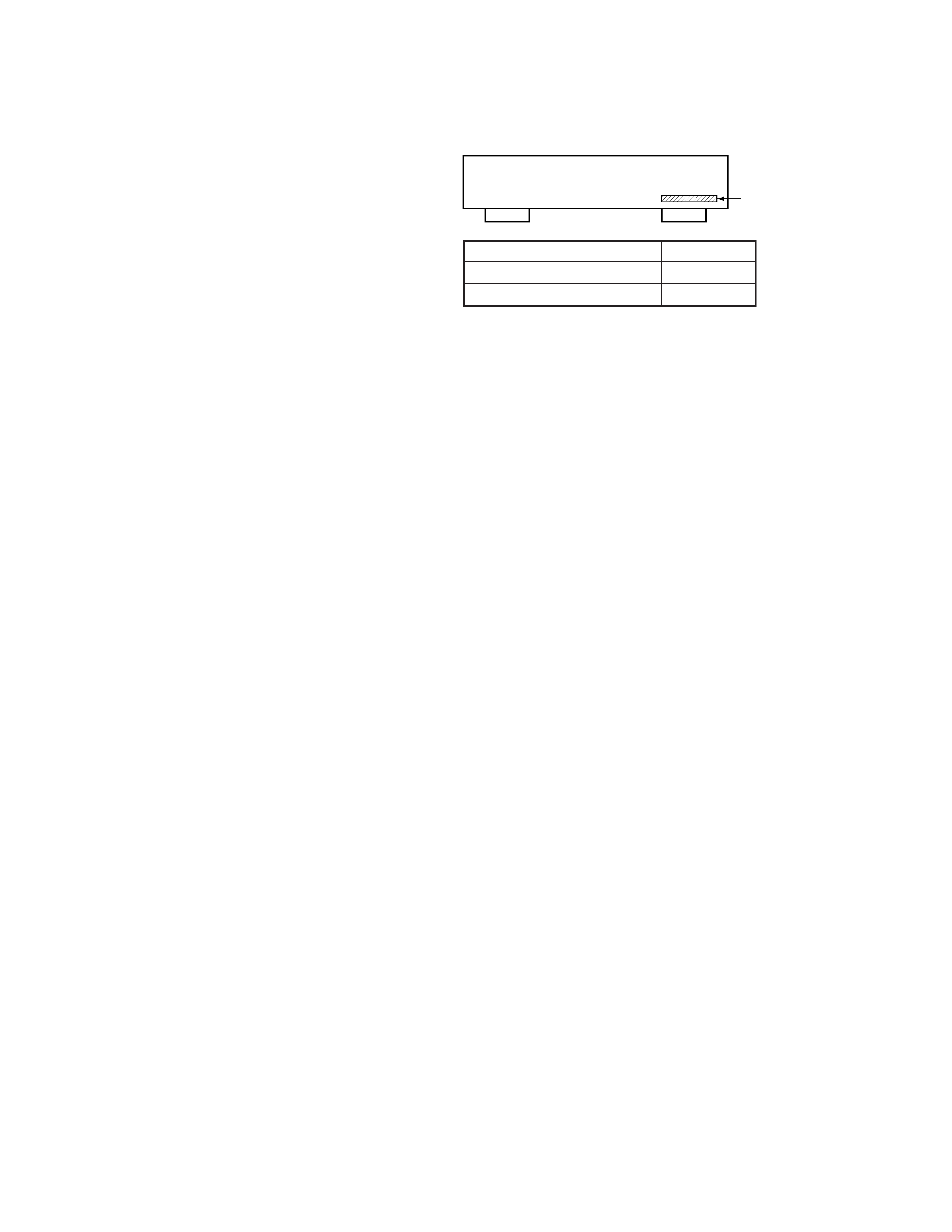
This appliance is classified as a
CLASS 1 LASER product.
The CLASS 1 LASER
PRODUCT MARKING is
located on the rear exterior.
This caution label
is located inside
the unit.
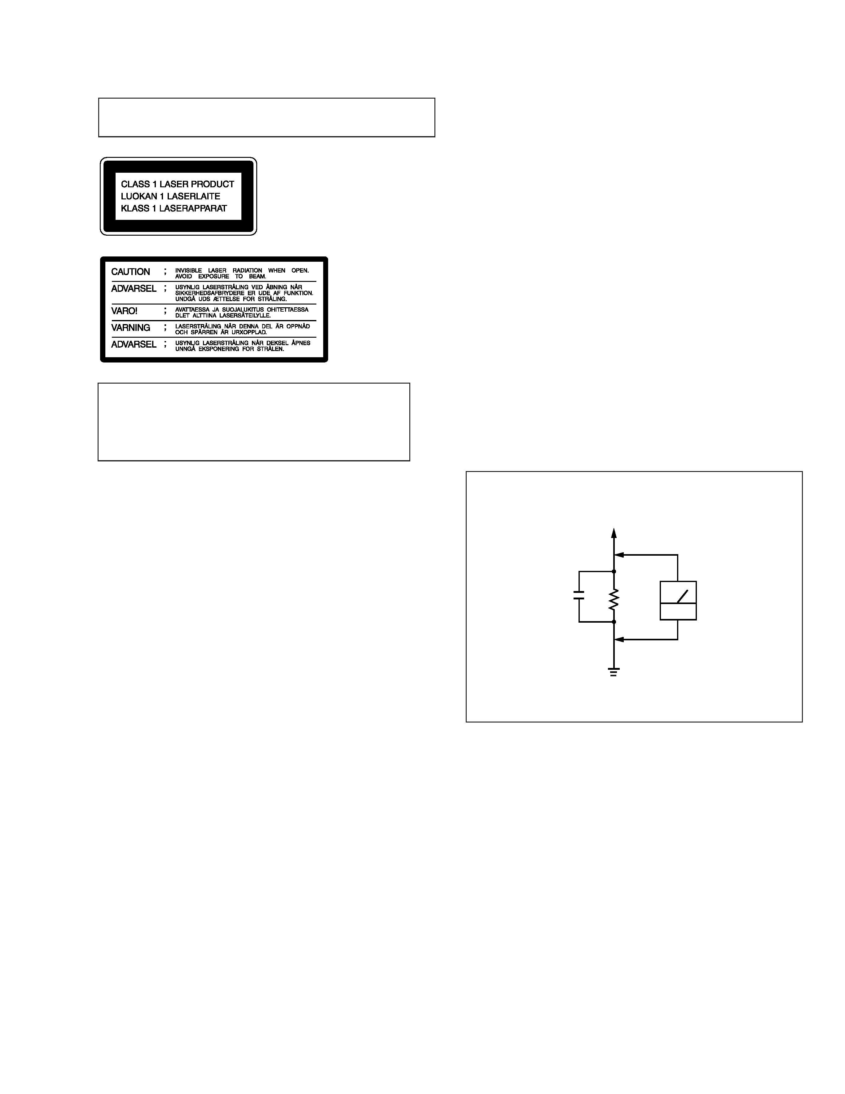
Fig. A. Using an AC voltmeter to check AC leakage.
To Exposed Metal
Parts on Set
0.15
µF
1.5k
AC
voltmeter
(0.75V)
Earth Ground
-- 4 --
Power Supply During Servicing
This unit is not able to operate on its own because it does not have its own power supply. During servicing, connect to other units.
Power is supplied when the SYSTEM POWER button of the amplifier (TA-M7) is turned ON.
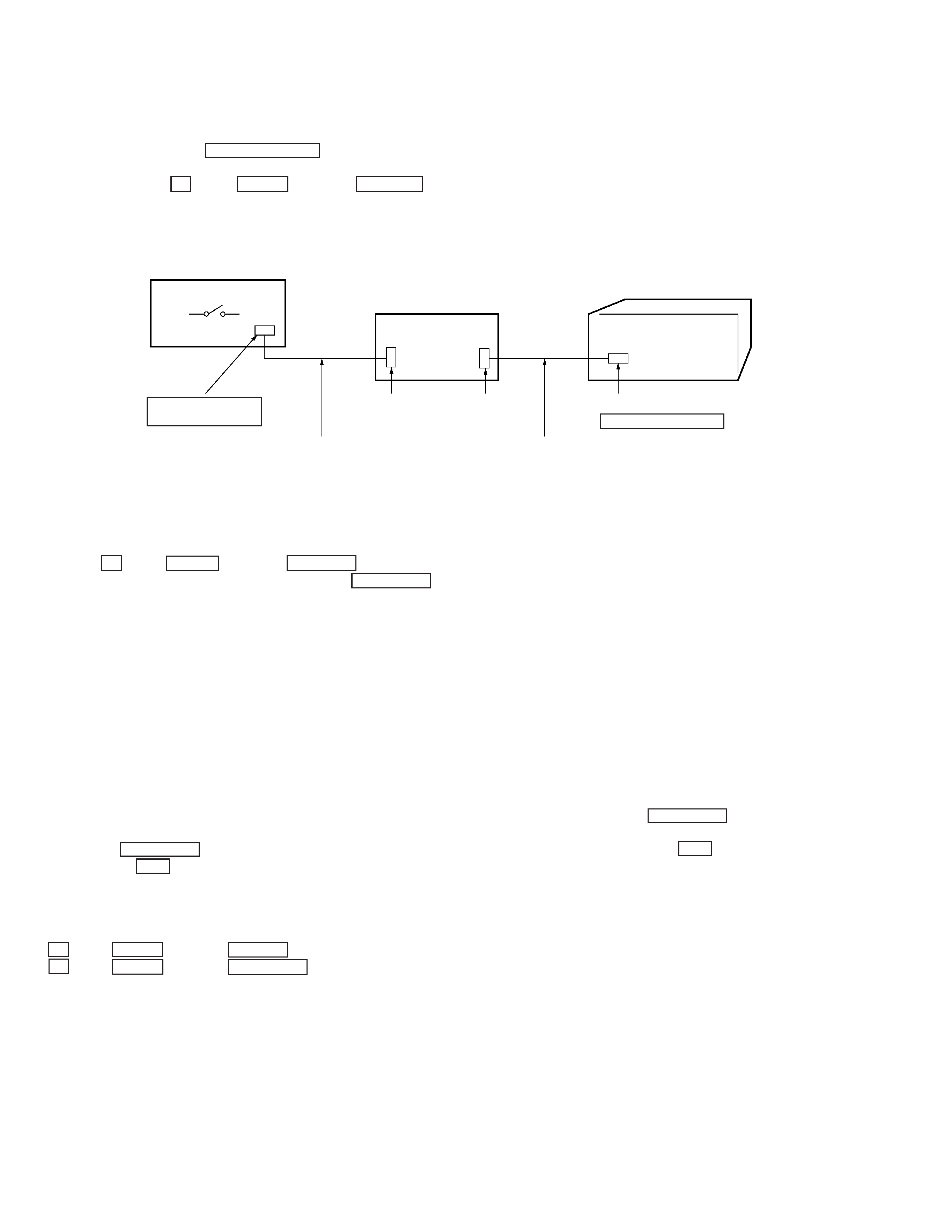
If the other units are not available, use a service box (PFJ-1) and jig (J-2501-078-A).
In this case, press the
p button, r REC button, and DISPLAY button simultaneously to turn on the power.
[Connection Diagram]
SECTION 1
SERVICE NOTE
KEY/Fluorescent Indicator Tube/LED Check Mode
Press the
p button, r REC button, and SHUFFLE button simultaneously to turn on the key/Fluorescent indicator tube/LED check mode.
During the check mode, press any button or rotate the SELECTOR knob to proceed onto the next step.
1 LED all-lit mode (displays KEY/FL/LED.)
2 Fluorescent indicator tube all lit mode
3 CHECK 1 lit mode (partially lit)
4 CHECK 2 lit mode (Partially lit)
5 Key check mode (Displays JOG = 0, KEY = 0)
Note 1) When the three buttons pressed to enter the LED all lit mode are released together, the LED all lit mode will remain on. When released
separately, the next Fluorescent indicator tube all lit mode will be set.
Note 2) The LEDs will light up sequentially after the all lit mode each time the buttons are pressed or the SELECTOR knob is rotated.
Note 3) In the key check mode, each time the button is pressed, the "KEY =" number on the Fluorescent indicator tube increases. When
the SELECTOR knob is rotated, the "JOG =" number on the Fluorescent indicator tube increases in the
+ direction and decreases
in the
= direction.
Note 4) To end the above mode, remove the amplifier AC plug or turn OFF the PFJ-1 POWER switch.
Input Switching by Multiple Pressing
The desired input switching can be performed by the following multiple pressing.
p button, r REC button, and REPEAT button : Digital-in
p button, r REC button, and CONTINUE button : Analog-in
CN101
SERVICE BOX (PFJ-1)
POWER SW
JIG
(J-2501-078-A)
Unit (MDS-M9)
Connector cable 17P
(Provided with PFJ-1)
Connector cable 7P
(Provided with unit)
CN902
7P
SYSTEM CONTROL
FH-E939, 838, 937
CDP/TC
CN904
17P
N
N
N
N