SERVICE MANUAL
LEVEL
2
Link
SERVICE NOTE
DISASSEMBLY
BLOCK DIAGRAMS
FRAME SCHEMATIC DIAGRAMS
SCHEMATIC DIAGRAMS
PRINTED WIRING BOARDS
ADJUSTMENTS
REPAIR PARTS LIST
SPECIFICATIONS
SERVICE NOTE
DISASSEMBLY
BLOCK DIAGRAMS
FRAME SCHEMATIC DIAGRAMS
SCHEMATIC DIAGRAMS
PRINTED WIRING BOARDS
ADJUSTMENTS
REPAIR PARTS LIST
SPECIFICATIONS
Link
On the VC-283 board
This service manual provides the information that is premised the circuit board replacement service and not intended repair
inside the VC-283 board.
Therefore, schematic diagram, printed wiring board, waveforms, mounted parts location and electrical parts list of the VC-283
board are not shown.
The following pages are not shown.
Schematic diagram ............................. Pages 4-33 to 4-70
Printed wiring board ............................ Pages 4-89 to 4-92
Waveforms ........................................... Pages 4-94 to 4-95
Mounted parts location ............................. Pages 4-98 to 4-99
Electrical parts list ................................... Pages 6-18 to 6-25
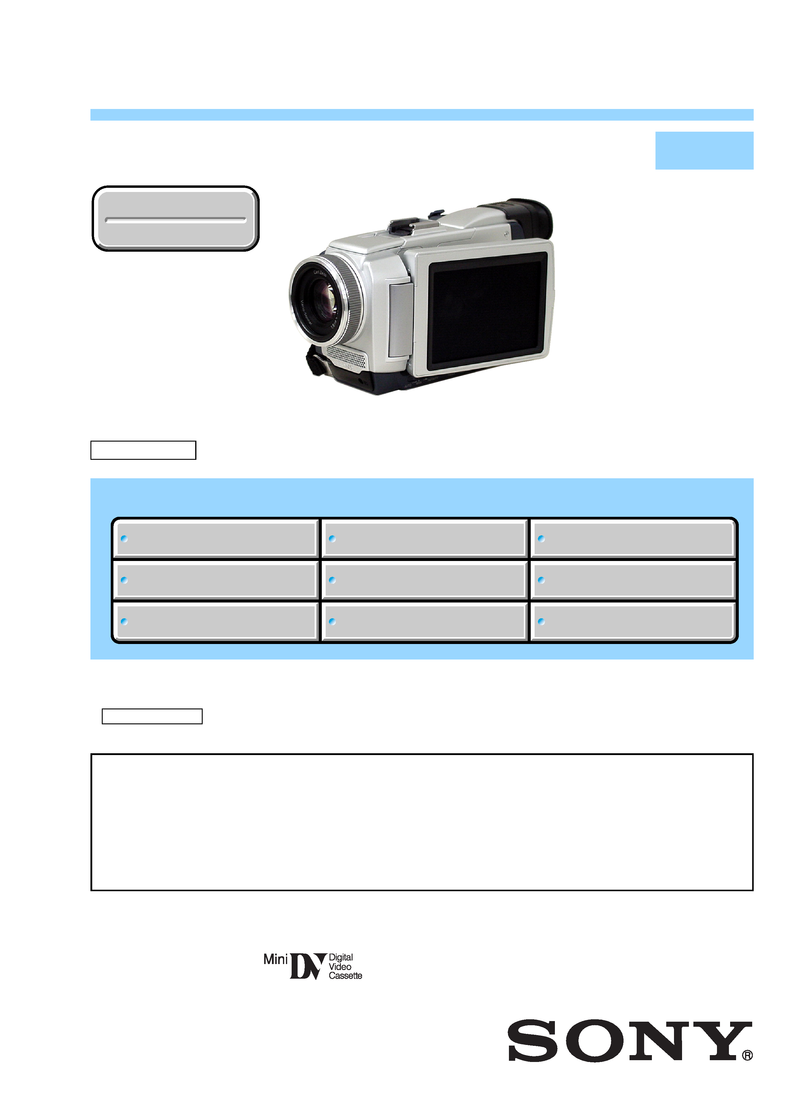
DCR-TRV40/TRV40E/
TRV50/TRV50E
RMT-811
US Model
Canadian Model
DCR-TRV50
AEP Model
East European Model
DCR-TRV40E/TRV50E
UK Model
Australian Model
DCR-TRV50E
E Model
DCR-TRV40/TRV40E/TRV50/TRV50E
Hong Kong Model
DCR-TRV40/TRV50E
Tourist Model
DCR-TRV40/TRV40E
Korea Model
DCR-TRV40
Chinese Model
DCR-TRV40E
J MECHANISM
Revision History
Revision History
Ver 1.3 2003. 11
· For INSTRUCTION MANUAL, refer to separate file (992995171.pdf).
· For MECHANISM ADJUSTMENTS, refer to the "DV MECHANICAL ADJUSTMENT MANUAL VI
J MECHANISM " (9-929-807-11).
· HOW TO OPEN THE FLASH WHEN THE FLASH DOESN'T OPEN
DIGITAL VIDEO CAMERA RECORDER
Photo: DCR-TRV50E

-- 2 --
DCR-TRV40/TRV40E/TRV50/TRV50E
SPECIFICATIONS
SAFETY-RELATED COMPONENT WARNING!!
COMPONENTS IDENTIFIED BY MARK 0 OR DOTTED LINE WITH
MARK 0 ON THE SCHEMATIC DIAGRAMS AND IN THE PARTS
LIST ARE CRITICAL TO SAFE OPERATION. REPLACE THESE
COMPONENTS WITH SONY PARTS WHOSE PART NUMBERS
APPEAR AS SHOWN IN THIS MANUAL OR IN SUPPLEMENTS
PUBLISHED BY SONY.
ATTENTION AU COMPOSANT AYANT RAPPORT
À LA SÉCURITÉ!
LES COMPOSANTS IDENTIFÉS PAR UNE MARQUE 0 SUR LES
DIAGRAMMES SCHÉMATIQUES ET LA LISTE DES PIÈCES SONT
CRITIQUES POUR LA SÉCURITÉ DE FONCTIONNEMENT. NE
REMPLACER CES COMPOSANTS QUE PAR DES PIÈSES SONY
DONT LES NUMÉROS SONT DONNÉS DANS CE MANUEL OU
DANS LES SUPPÉMENTS PUBLIÉS PAR SONY.
COVER
COVER
CAUTION :
Danger of explosion if battery is incorrectly replaced.
Replace only with the same or equivalent type.
Video camera
recorder
System
Video recording system
2 rotary heads
Helical scanning system
Audio recording system
Rotary heads, PCM system
Quantization: 12 bits (Fs 32 kHz,
stereo 1, stereo 2), 16 bits
(Fs 48 kHz, stereo)
Video signal
PAL colour, CCIR standards
DCR-TRV40/TRV50:
NTSC colour, EIA standards
DCR-TRV40E/TRV50E:
DCR-TRV40/TRV50:
Chrominance signal: 0.3 Vp-p,
DCR-TRV40E/TRV50E:
Usable cassette
Mini DV cassette with the
mark printed
Tape speed
SP: Approx. 18.81 mm/s
LP: Approx. 12.56 mm/s
Recording/playback time
(using cassette DVM60)
SP: 1 hour
LP: 1.5 hours
Fastforward/rewind time
(using cassette DVM60)
When using the battery pack:
Approx. 2 min. and 30 seconds
When using the AC power adaptor:
Approx. 1 min. and 45 seconds
Viewfinder
Electric viewfinder (colour)
Image device
4.5 mm (1/4 type) CCD (Charge
Coupled Device)
Gross: Approx. 1 550 000 pixels
Effective (still):
Approx. 1 390 000 pixels
Effective (moving):
Approx. 970 000 pixels
Lens
Carl Zeiss Vario-Sonnar
Combined power zoom lens
Filter diameter: 37 mm
(1 1/2 in)
10
× (Optical), 120× (Digital)
F=1.8~2.2
Focal length
4.2 42 mm (3/16 1 11/16 in.)
When converted to a 35 mm still
camera
In CAMERA:
48 480 mm (1 15/16 19 in.)
In MEMORY:
40 400 mm (1 5/8 15 3/4 in.)
Colour temperature
Auto, HOLD (Hold), nIndoor
(3 200 K),
Outdoor (5 800 K)
Minimum illumination
7 lx (lux) (F 1.8)
0 lx (lux) (in the NightShot mode)*
* Objects unable to be seen due to
the dark can be shot with infrared
lighting.
Input/Output connectors
S video input/output
4-pin mini DIN
Luminance signal: 1 Vp-p,
75
(ohms), unbalanced
Chrominance signal: 0.3 Vp-p,
75
(ohms), unbalanced
Audio/Video input/output
AV MINI JACK, 1 Vp-p,
75
(ohms), unbalanced, sync
negative
327 mV, (at output impedance
more than 47 k
(kilohms))
Output impedance with less than
2.2 k
(kilohms)/Stereo minijack (ø
3.5 mm)
Input impedance more than
47 k
(kilohms)
DV input/output
4-pin connector
Headphone jack
Stereo minijack (ø 3.5 mm)
LANC jack
Stereo mini-minijack (ø 2.5 mm)
USB jack
mini-B
MIC jack
Minijack, 0.388 mV low impedance
with 2.5 to 3.0 V DC, output
impedance 6.8 k
(kilohms) (ø 3.5
mm)
Stereo type
LCD screen
Picture
8.8 cm (3.5 type)
72.2
× 50.4 mm (2 4/5 × 2 in.)
Total dot number
246 400 (1 120
× 220)
Wireless communications
(DCR-TRV50/TRV50E only)
Communications system
Bluetooth standard Ver.1.1
Max. baud rate1) 2)
Approx. 723 kbps
Output
Bluetooth standard Power Class 2
Communications distance2)
Max. wireless distance Approx. 10
m (393 3/4 in.) (When connecting to
BTA-NW1)
Compatible Bluetooth profile3)
Generic Access Profile
Dial-up Networking Profile
Operating frequency band
2.4 GHz band (2.400 GHz
2.483 5 GHz)
1)
Max. baud rate of Bluetooth
standard Ver.1.1
2)
Varies according to the distance
between communicating devices,
presence of obstacles, radiowave
conditions, and other factors.
3)
This is a specification matched to
specific usage requirements
between Bluetooth compatible
devices. It is laid down in the
Bluetooth standards.
General
Power requirements
7.2 V (battery pack)
8.4 V (AC power adaptor)
Average power consumption
(when using the battery pack)
During camera recording using
LCD
4.4 W
Viewfinder
3.3 W
Operating temperature
0
°C to 40°C (32°F to 104°F)
Storage temperature
20
°C to + 60°C
(4
°F to + 140°F)
Dimensions (Approx.)
72
× 91 × 168 mm
(2 7/8
× 3 5/8 × 6 5/8 in.) (w/h/d)
Mass (Approx.)
700 g (1 lb 8 oz)
main unit only
800 g (1 lb 12 oz)
including the battery pack
NP-FM50, cassette DVM60 and lens
cap
Supplied accessories
See page 3.
AC power adaptor
Power requirements
100 240 V AC, 50/60 Hz
Power consumption
23 W
Output voltage
DC OUT: 8.4 V, 1.5 A in the
operating mode
Operating temperature
0
°C to 40°C (32°F to 104°F)
Storage temperature
20
°C to + 60°C
(4
°F to + 140°F)
Dimensions (approx.)
125
× 39 × 62 mm
(5
× 1 9/16 × 2 1/2 in.) (w/h/d)
excluding projecting parts
Mass (approx.)
280 g (9.8 oz)
excluding mains lead
Battery pack
Maximum output voltage
DC 8.4 V
Output voltage
DC 7.2 V
Capacity
8.5 Wh (1 180 mAh)
Dimensions (approx.)
38.2
× 20.5 × 55.6 mm
(1 9/16
× 13/16 × 2 1/4 in.)
(w/h/d)
Mass (approx.)
76 g (2.7 oz)
Type
Lithium ion
"Memory Stick"
Memory
Flash memory
8MB: MSA-8A
Operating voltage
2.7 3.6 V
Power consumption
Approx. 45 mA in the operating
mode
Approx. 130
µA in the standby
mode
Dimensions (approx.)
50
× 2.8 × 21.5 mm
(2
× 1/8 × 7/8 in.) (w/h/d)
Mass (approx.)
4 g (0.14 oz)
Design and specifications are
subject to change without notice.
-- 3 --
DCR-TRV40/TRV40E/TRV50/TRV50E
1.
Check the area of your repair for unsoldered or poorly-soldered
connections. Check the entire board surface for solder splashes
and bridges.
2.
Check the interboard wiring to ensure that no wires are
"pinched" or contact high-wattage resistors.
3.
Look for unauthorized replacement parts, particularly
transistors, that were installed during a previous repair. Point
them out to the customer and recommend their replacement.
4.
Look for parts which, through functioning, show obvious signs
of deterioration. Point them out to the customer and
recommend their replacement.
5.
Check the B+ voltage to see it is at the values specified.
6.
Flexible Circuit Board Repairing
· Keep the temperature of the soldering iron around 270°C
during repairing.
· Do not touch the soldering iron on the same conductor of the
circuit board (within 3 times).
· Be careful not to apply force on the conductor when soldering
or unsoldering.
Unleaded solder
Boards requiring use of unleaded solder are printed with the lead-
free mark (LF) indicating the solder contains no lead.
(Caution: Some printed circuit boards may not come printed with
the lead free mark due to their particular size.)
: LEAD FREE MARK
Unleaded solder has the following characteristics.
· Unleaded solder melts at a temperature about 40
°C higher than
ordinary solder.
Ordinary soldering irons can be used but the iron tip has to be
applied to the solder joint for a slightly longer time.
Soldering irons using a temperature regulator should be set to
about 350
°C.
Caution: The printed pattern (copper foil) may peel away if the
heated tip is applied for too long, so be careful!
· Strong viscosity
Unleaded solder is more viscous (sticky, less prone to flow) than
ordinary solder so use caution not to let solder bridges occur such
as on IC pins, etc.
· Usable with ordinary solder
It is best to use only unleaded solder but unleaded solder may
also be added to ordinary solder.
SAFETY CHECK-OUT
After correcting the original service problem, perform the following
safety checks before releasing the set to the customer.
9
1
4
q;
5
qa
qg
qh
6
qs
2
7
qd
3
8
qf
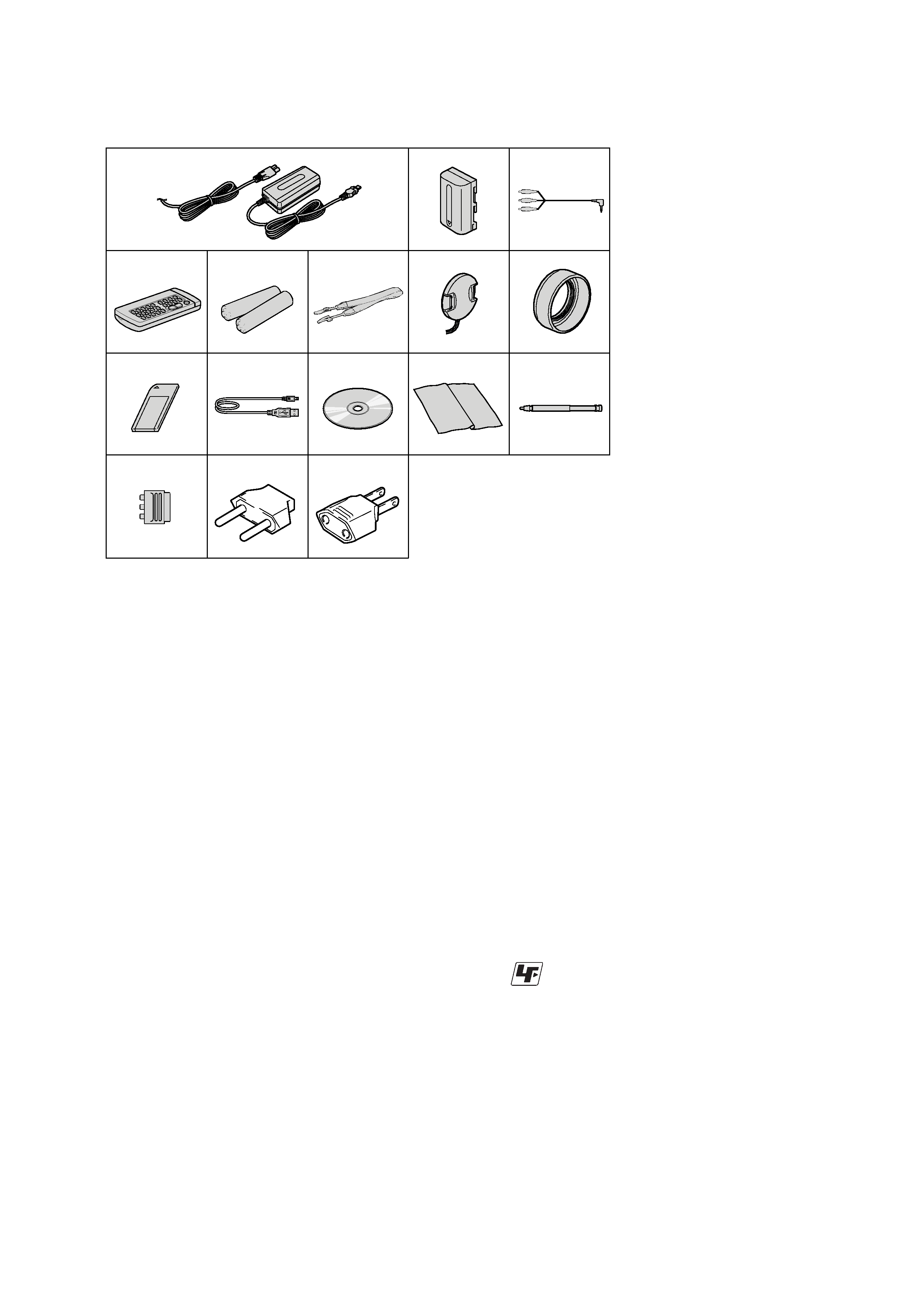
1
AC-L10A/L10B/L10C AC power adaptor (1),
mains lead (1)
2
NP-FM50 battery pack (1)
3
A/V connecting cable (1)
4
Wireless Remote Commander (1)
5
Size R6 (size AA) battery for Remote
Commander (2)
6
Shoulder strap (1)
7
Lens cap (1)
8
Lens hood (1)
9
"Memory Stick" (1)
0
USB cable (1)
qa
CD-ROM (USB Driver) (1)
qs
Cleaning cloth (1)
qd
Stylus (1) (DCR-TRV50/TRV50E only)
qf
21-pin adaptor (European models only) (1)
qg
2-pin conversion adaptor (1)
(Tourist model only)
SPVD-008 (Except US, Canadian model only)
SPVD-008 (I) (US, Canadian model only)
qh
2-pin conversion adaptor (1)
(E, Hong Kong model only)
· SUPPLIED ACCESSORIES
Make sure that the following accessories are supplied with your camcorder.

-- 4 --
DCR-TRV40/TRV40E/TRV50/TRV50E
TABLE OF CONTENTS
1.
SERVICE NOTE
1-1.
SERVICE NOTE ····························································· 1-1
1.
POWER SUPPLY DURING REPAIRS ·························· 1-1
2.
HOW TO OPEN THE FLASH WHEN THE FLASH
DOESN'T OPEN ···························································· 1-1
3.
TO TAKE OUT A CASSETTE WHEN NOT EJECT
(FORCE EJECT) ····························································· 1-1
4.
DISCHARGING OF THE FLASHLIGHT POWER
SUPPLY CAPACITOR ··················································· 1-2
4-1.
PREPARING THE SHORT JIG ······································ 1-2
4-2.
DISCHARGING THE CAPACITOR ······························ 1-2
1-2.
SELF-DIAGNOSIS FUNCTION ···································· 1-3
1.
SELF-DIAGNOSIS FUNCTION ···································· 1-3
2.
SELF-DIAGNOSIS DISPLAY ······································· 1-3
3.
SERVICE MODE DISPLAY ·········································· 1-3
3-1.
Display Method ······························································· 1-3
3-2.
Switching of Backup No. ················································ 1-3
3-3.
End of Display ································································· 1-3
4.
SELF-DIAGNOSIS CODE TABLE ································ 1-4
2.
DISASSEMLY
2-1.
LCD SECTION (PD-165 BOARD) ································ 2-3
2-2.
EVF SECTION (LB-078 BOARD) ································· 2-4
2-3.
TOP CABINET ······························································· 2-5
2-4.
FRONT PANEL SECTION ············································· 2-6
2-5.
MA-408 BOARD ···························································· 2-7
2-6.
CABINET (R) SECTION (1) ·········································· 2-8
2-7.
CABINET (R) SECTION (2) ·········································· 2-8
2-8.
BATTERY SECTION ····················································· 2-9
2-9.
BT-003 BOARD (TRV50/TRV50E) ······························· 2-9
2-10. EXTERNAL CONNECTOR (HOT SHOE) ················· 2-10
2-11. DD HEAT SINK ···························································· 2-10
2-12. EVF SECTION ······························································ 2-11
2-13. FLASH UNIT (FLASH SECTION) (1) ························ 2-11
2-14. FLASH UNIT (FLASH SECTION) (2) ························ 2-12
2-15. FLASH UNIT (FLASH SECTION) (3) ························ 2-12
2-16. FLASH UNIT (FLASH SECTION) (4) ························ 2-13
2-17. DD-176 BOARD ··························································· 2-14
2-18. VC-283 BOARD, MECHANISM DECK (1) ··············· 2-15
2-19. VC-283 BOARD, MECHANISM DECK (2) ··············· 2-15
2-20. VC-283 BOARD, MECHANISM DECK (3) ··············· 2-16
2-21. LENS SECTION ··························································· 2-16
2-22. JK-219 BOARD ···························································· 2-17
2-23. CD-381 BOARD, 690C (CZ) BLOCK ASSEMBLY
(LENS DEVICE) ··························································· 2-17
2-24. CS FRAME ASSEMBLY ·············································· 2-20
2-25. FLASH UNIT ································································ 2-20
2-26. CONTROL SWITCH BLOCK (PS-2890) ···················· 2-21
2-27. MEMORY STICK CONNECTOR ······························· 2-21
2-28. CK-115 BOARD, SPEAKER (2.0CM) ························· 2-22
2-29. HINGE SECTION ························································· 2-22
2-30. HINGE ASSEMBLY ····················································· 2-23
2-31. CIRCUIT BOARDS LOCATION ································· 2-24
2-32. FLEXIBLE BOARDS LOCATION ······························ 2-25
3.
BLOCK DIAGRAMS
3-1.
OVERALL BLOCK DIAGRAM (1/4) ··························· 3-1
3-2.
OVERALL BLOCK DIAGRAM (2/4) ··························· 3-3
3-3.
OVERALL BLOCK DIAGRAM (3/4) ··························· 3-5
3-4.
OVERALL BLOCK DIAGRAM (4/4) ··························· 3-7
3-5.
POWER BLOCK DIAGRAM (1/2) ································ 3-9
3-6.
POWER BLOCK DIAGRAM (2/2) ······························ 3-11
4.
PRINTED WIRING BOARDS AND
SCHEMATIC DIAGRAMS
4-1.
FRAME SCHEMATIC DIAGRAM (1/4) ······················· 4-1
FRAME SCHEMATIC DIAGRAM (2/4) ······················· 4-3
FRAME SCHEMATIC DIAGRAM (3/4) ······················· 4-5
FRAME SCHEMATIC DIAGRAM (4/4) ······················· 4-7
4-2.
SCHEMATIC DIAGRAMS ·········································· 4-11
· CD-381 (CCD IMAGER)
SCHEMATIC DIAGRAM ···························· 4-11
· JK-219 (AV IN/OUT, STEADY SHOT)
SCHEMATIC DIAGRAM ···························· 4-13
· CK-115 (CONTROL SWITCH)
SCHEMATIC DIAGRAM ···························· 4-15
· FK-2890, PS-2890 (CONTROL SWITCH BLOCK), FP-
460 FLEXIBLE
SCHEMATIC DIAGRAM ··························· 4-17
· MA-408 (1/2)(MIC AMP, REMOTE COMMANDER
RECEIVER)
SCHEMATIC DIAGRAM ···························· 4-19
· MA-408 (2/2)(LANC, EXT MIC)
SCHEMATIC DIAGRAM ···························· 4-21
· PD-165 (1/2)(RGB DRIVE, TIMING GENERATOR)
SCHEMATIC DIAGRAM ···························· 4-23
· PD-165 (2/2)(LCD DRIVER, BACK LIGHT)
SCHEMATIC DIAGRAM ···························· 4-25
· DD-176 (1/2)(DC/DC CONVERTER)
SCHEMATIC DIAGRAM ···························· 4-27
· DD-176 (2/2)(CONNECTOR)
SCHEMATIC DIAGRAM ···························· 4-29
· FP-100 (MODE SWITCH), FP-228 (DEW SENSOR),
FP-102 (TAPE TOP/END SENSOR, S/T REEL)
FLEXIBLE BOARD ····································· 4-31
Shematic diagram of the VC-283 board are not shown.
Pages from 4-33 to 4-70 are not shown.
4-3.
PRINTED WIRING BOARDS ····································· 4-71
· CD-381 (CCD IMAGER)
PRINTED WIRING BOARD ······················· 4-71
· FP-460 FLEXIBLE BOARD ····································· 4-72
· JK-219 (AV IN/OUT, STEADY SHOT)
PRINTED WIRING BOARD ······················· 4-73
· CK-115 (CONTROL SWITCH)
PRINTED WIRING BOARD ······················· 4-77
· MA-408 (MIC AMP, REMOTE COMMANDER
RECEIVER, LANC, EXT MIC)
PRINTED WIRING BOARD ······················· 4-79
· FP-461 FLEXIBLE BOARD ····································· 4-81
· SE-124 (MF-SENSOR)
PRINTED WIRING BOARD ······················· 4-82
· PD-165 (RGB DRIVE, TIMING GENERATOR, LCD
DRIVER, BACK LIGHT)
PRINTED WIRING BOARD ······················· 4-83
· DD-176 (DC/DC CONVERTER, CONNECTOR)
PRINTED WIRING BOARD ······················· 4-85
· FP-100 (MODE SWITCH), FP-228 (DEW SENSOR),
FP-102 (TAPE TOP/END SENSOR, S/T REEL)
FLEXIBLE BOARDS ··································· 4-87
· LB-078 (EVF BACK LIGHT)
PRINTED WIRING BOARD ······················· 4-87
Printed wiring board of the VC-283 board are not shown.
Pages from 4-89 to 4-92 are not shown.
4-4.
WAVEFORMS ······························································ 4-93
Waveforms of the VC-283 board are not shown.
Pages from 4-94 to 4-95 are not shown.

-- 5 --
DCR-TRV40/TRV40E/TRV50/TRV50E
4-5.
MOUNTED PARTS LOCATION ································· 4-96
Mounted parts location of the VC-283 board is not shown.
Pages from 4-98 to 4-99 are not shown.
5.
ADJUSTMENT
1.
Adjusting items when replacing main parts and boards. ··· 5-2
5-1.
CAMERA SECTION ADJUSTMENT ··························· 5-4
1-1.
PREPARATIONS BEFORE ADJUSTMENT
(CAMERA SECTION) ··················································· 5-4
1-1-1. List of Service Tools ························································ 5-4
1-1-2. Preparations ····································································· 5-5
1-1-3. Precaution ········································································ 5-7
1.
Setting the Switch ···························································· 5-7
2.
Order of Adjustments ······················································ 5-7
3.
Subjects ··········································································· 5-7
1-2.
INITIALIZATION OF 8, A, B, C, D, E, F, 1B, 1E, 1F
PAGE DATA ···································································· 5-8
1-2-1. INITIALIZATION OF A, D PAGE DATA ······················ 5-9
1.
Initializing the A, D Page Data ········································ 5-9
2.
Modification of A, D Page Data ······································ 5-9
3.
A Page Table ···································································· 5-9
4.
D Page Table ·································································· 5-10
1-2-2. INITIALIZATION OF B, 1B PAGE DATA ·················· 5-11
1.
Initializing the B, 1B Page Data ···································· 5-11
2.
Modification of B, 1B Page Data ·································· 5-11
3.
Loader Writing Inhibit Mode Setting ···························· 5-11
4.
Writing the Network Default Setting Value
(DCR-TRV50/TRV50E) ················································ 5-11
5.
B Page Table ·································································· 5-12
6.
1B Page Table ································································ 5-12
1-2-3. INITIALIZATION OF 8, C PAGE DATA ····················· 5-13
1.
Initializing the 8, C Page Data ······································· 5-13
2.
Modification of 8, C Page Data ····································· 5-13
3.
8 Page Table ··································································· 5-13
4.
C Page Table ·································································· 5-14
1-2-4. INITIALIZATION OF E, F, 1E, 1F PAGE DATA ········ 5-16
1.
Initializing the E, F, 1E, 1F Page Data ·························· 5-16
2.
Modification of E, F, 1E, 1F Page Data ························· 5-16
3.
E Page Table ·································································· 5-17
4.
F Page Table ·································································· 5-18
5.
1E Page Table ································································ 5-19
6.
1F Page Table ································································ 5-20
1-3.
CAMERA SYSTEM ADJUSTMENTS ························ 5-21
1.
40.5MHz/54MHz Origin Oscillation Adjustment
(VC-283 board) ····························································· 5-21
2.
HALL Adjustment ························································· 5-22
3.
MAX GAIN Adjustment ··············································· 5-23
4.
CCD Output 2ch Matching Adjustment (1) ·················· 5-23
5.
CCD Output 2ch Matching Adjustment (2) ·················· 5-24
6.
MR Adjustment ····························································· 5-24
7.
Flange Back Adjustment (Using Minipattern Box) ······· 5-25
8.
Flange Back Adjustment (Using Flange Back Adjustment
Chart and Subject More Than 500m Away) ················· 5-26
8-1.
Flange Back Adjustment (1) ·········································· 5-26
8-2.
Flange Back Adjustment (2) ·········································· 5-26
9.
Flange Back Check ························································ 5-27
10.
Picture Frame Setting ···················································· 5-27
11.
Color Reproduction Adjustment ···································· 5-28
12.
Auto White Balance & LV Standard Data Input ··········· 5-29
13.
Auto White Balance Adjustment ··································· 5-30
14.
White Balance Check ···················································· 5-31
15.
Mechanical Shutter Adjustment ···································· 5-32
16.
Black Defective CCD Adjustment ································· 5-32
17.
Strobe Light Level Adjustment ····································· 5-33
18.
Strobe White Balance Adjustment & Check ················· 5-33
19.
AF Laser Output Adjustment ········································ 5-34
20.
AF Laser Check ····························································· 5-35
21.
Steady Shot Check ························································· 5-36
1-4.
COLOR ELECTRONIC VIEWFINDER SYSTEM
ADJUSTMENT ····························································· 5-37
1.
VCO Adjustment (VC-283 board) ································ 5-37
2.
RGB AMP Adjustment (VC-283 board) ······················· 5-38
3.
Contrast Adjustment (VC-283 board) ··························· 5-38
4.
Backlight Adjustment (VC-283 board) ························· 5-39
5.
White Balance Adjustment (VC-283 board) ················· 5-39
1-5.
LCD SYSTEM ADJUSTMENT ··································· 5-40
1.
VCO Adjustment (PD-165 board) ································· 5-40
2.
RGB AMP Adjustment (PD-165 board) ························ 5-41
3.
Contrast Adjustment (PD-165 board) ···························· 5-41
4.
COM AMP Adjustment (PD-165 board) ······················· 5-42
5.
V COM Adjustment (PD-165 board) ···························· 5-42
6.
White Balance Adjustment (PD-165 board) ·················· 5-43
5-2.
MECHANISM SECTION ADJUSTMENT ·················· 5-44
2-1.
HOE TO ENTER RECORD MODE WITHOUT
CASSETTE ··································································· 5-44
2-2.
HOE TO ENTER PLAYBACK MODE WITHOUT
CASSETTE ··································································· 5-44
2-3.
TAPE PATH ADJUSTMENT ········································ 5-44
1.
Preparation for Adjustment ··········································· 5-44
2.
Processing after Completing Operations: ······················ 5-44
5-3.
VIDEO SECTION ADJUSTMENT ······························ 5-45
3-1.
PREPARATIONS BEFORE ADJUSTMENTS ············ 5-45
3-1-1. Equipment to Required ·················································· 5-45
3-1-2. Precautions on Adjusting ··············································· 5-46
3-1-3. Adjusting Connectors ···················································· 5-47
3-1-4. Connecting the Equipment ············································ 5-47
3-1-5. Alignment Tapes ···························································· 5-48
3-1-6. Input/Output Level and Impedance ······························· 5-48
3-2.
SYSTEM CONTROL SYSTEM ADJUSTMENT ········ 5-49
1.
Initialization of 8, A, B, C, D, E, F, 1B, 1E, 1F
Page Data ······································································· 5-49
2.
Touch Panel Adjustment ················································ 5-49
3.
Serial No. Input ····························································· 5-50
3-1.
Company ID Input ························································· 5-50
3-2.
Serial No. Input ····························································· 5-50
3-3.
SERVO AND RF SYSTEM ADJUSTMENT ··············· 5-52
1.
Cap FG Duty Adjustment (VC-283 Board) ··················· 5-52
2.
PLL f0 & LPF f0 Adjustment (VC-283 Board) ·············· 5-52
3.
Switching Position Adjustment (VC-283 Board) ·········· 5-53
4.
AGC Center Level and APC & AEQ Adjustment ········· 5-53
4-1.
Preparations before adjustments ···································· 5-53
4-2.
AGC Center Level Adjustment (VC-283 Board) ·········· 5-53
4-3.
APC & AEQ Adjustment (VC-283 Board) ··················· 5-54
4-4.
Processing after Completing Adjustments ···················· 5-54
5.
PLL f0 & LPF f0 Fine Adjustment (VC-283 Board) ······ 5-55
3-4.
VIDEO SYSTEM ADJUSTMENTS ····························· 5-56
1.
Chroma BPF fo Adjustment (VC-283 Board) ··············· 5-56
2.
S VIDEO OUT Y Level Adjustment (VC-283 Board) ···· 5-56
3.
S VIDEO OUT Chroma Level Adjustment
(VC-283 Board) ····························································· 5-57
4.
VIDEO OUT Y, Chroma Level Check (VC-283 Board) ·· 5-57
3-5.
AUDIO SYSTEM ADJUSTMENTS ···························· 5-58
1.
Playback Level Check ··················································· 5-59
2.
Overall Level Characteristics Check ····························· 5-59
3.
Overall Distortion Check ··············································· 5-59
4.
Overall Noise Level Check ············································ 5-59
5.
Overall Separation Check ·············································· 5-59
5-4.
SERVICE MODE ·························································· 5-60
4-1.
ADJUSTMENT REMOTE COMMANDER ················ 5-60
1.
Using the adjustment remote commander ····················· 5-60
2.
Precautions upon using the adjustment remote
commander ···································································· 5-60
4-2.
DATA PROCESS ··························································· 5-61