1
Ver 1.2 2004. 11
SERVICE MANUAL
US Model
Canadian Model
AEP Model
UK Model
E Model
CX-LZP5
Amplifier section
US, CND model:
Continuous RMS power output (reference):
20 + 20 W
(6 ohms at 1 kHz, 10%
THD)
Total harmonic distortion less than 0.9% (6 ohms at
1 kHz, 10 W)
AEP, UK model:
DIN power output (rated):
16 + 16 W
(6 ohms at 1 kHz, DIN)
Continuous RMS power output (reference):
20 + 20 W
(6 ohms at 1 kHz, 10%
THD)
Music power output (reference):
40 + 40 watts (6 ohms at
1 kHz, 10% THD)
SPECIFICATIONS
E51, MY, SP, TW model:
The following measured at 110 120, 220 240 V AC,
50/60 Hz
DIN power output (rated):
16 + 16 W
(6 ohms at 1 kHz, DIN)
Continuous RMS power output (reference):
20 + 20 W
(6 ohms at 1 kHz, 10%
THD)
Inputs
MD (RCA pin jacks):
Sensitivity 500 mV,
impedance 47 kilohms
Outputs
PHONES (stereo mini jack):
Accepts headphones with
an impedance of 8 ohms or
more
SPEAKERS:
Accepts impedance of
6 ohms
USB hub ports
Maximum current
consumption: 100 mA per
port
Sony Corporation
Personal Audio Company
Published by Sony Engineering Corporation
9-877-863-03
2004K04-1
© 2004. 11
Continued on next page
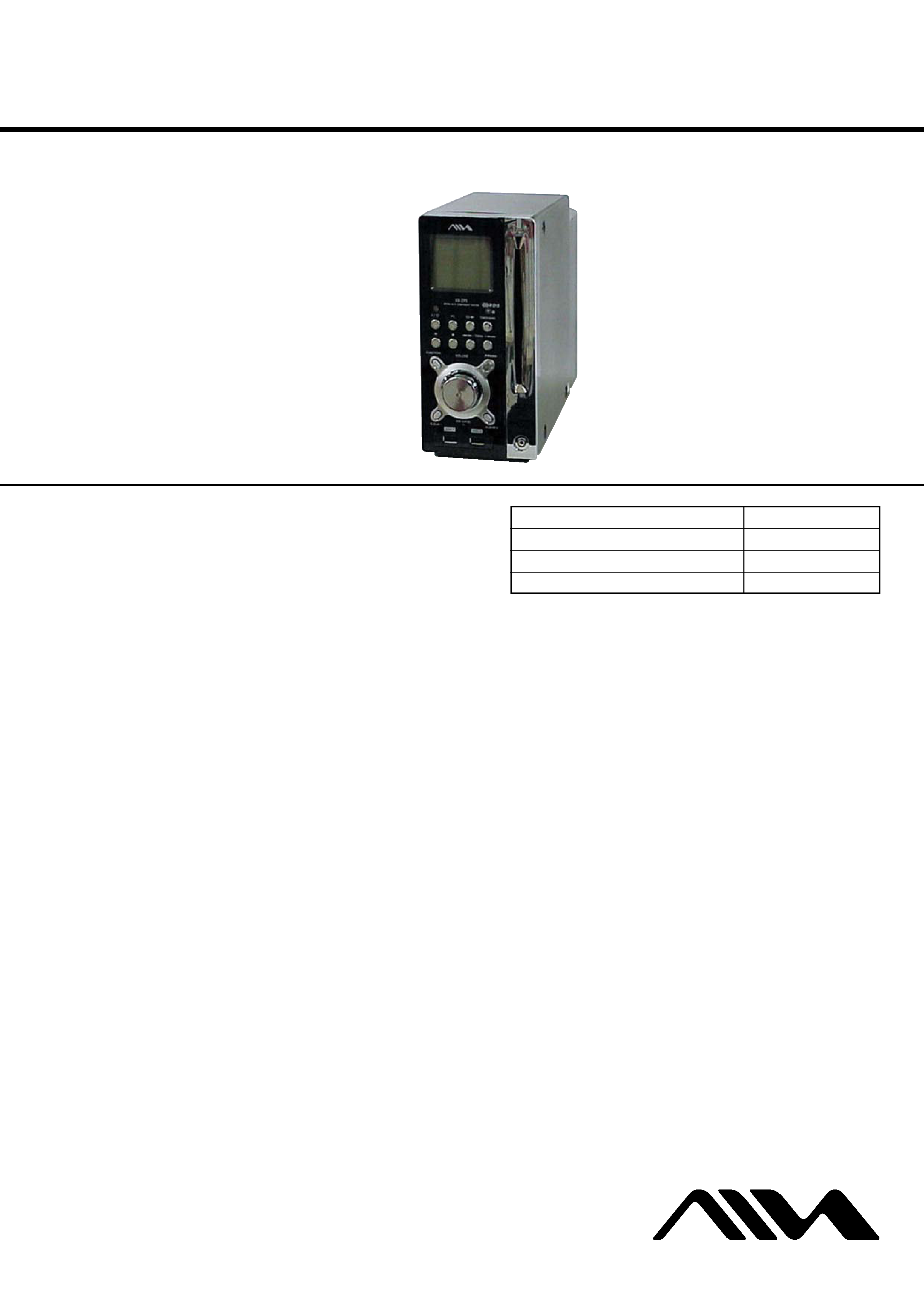
COMPACT DISC RECEIVER
· CX-LZP5 is compact disc receiver
in AWP-ZP5.
AUDIO POWER SPECIFICATIONS
(For the U.S. model)
POWER OUTPUT AND TOTAL HARMONIC
DISTORTION:
With 6-ohm loads, both channels driven, from
120 10,000 Hz: rated 20 watts per channel
minimum RMS power, with no more than 10%
total harmonic distortion from 250 milliwatts to
rated output.
Model Name Using Similar Mechanism
CX-LZP3
CD Mechanism Type
CDM80BV-F4BD81
Base Unit Name
BU-F4BD81B
Optical Pick-up Name
KSM-215CFP

2
CX-LZP5
CD player section
System
Compact disc and digital
audio system
Laser
Semiconductor laser
(
=780 nm)
Emission duration:
continuous
Frequency response
2 Hz 20 kHz
Tuner section
FM stereo, FM/AM superheterodyne tuner
FM tuner section
Tuning range
US, CND model:
87.5 108.0 MHz
(100-kHz step)
Other models:
87.5 108.0 MHz
(50-kHz step)
Antenna
FM lead antenna
Antenna terminals
75 ohms unbalanced
Intermediate frequency 10.7 MHz
AM tuner section
Tuning range
US, CND model:
530 1,710 kHz
(with the tuning interval
set at 10 kHz)
531 1,710 kHz
(with the tuning interval
set at 9 kHz)
AEP, UK model:
531 1,602 kHz
(with the tuning interval
set at 9 kHz)
E51, MY, SP, TW model: 530 1,710 kHz
(with the tuning interval
set at 10 kHz)
531 1,602 kHz
(with the tuning interval
set at 9 kHz)
Antenna
AM loop antenna, external
antenna terminal
Intermediate frequency 450 kHz
General
Power requirements
US, CND model:
120 V AC, 60 Hz
AEP, UK model:
230 V AC, 50/60 Hz
TW model:
120 V AC, 50/60 Hz
E51, MY, SP model:
110 120, 220 240 V
AC, 50/60 Hz
Adjustable with voltage
selector
Power consumption
AEP, UK model:
40 W
0.3 W (in Power Saving
mode)
US, CND model:
40 W
E51, MY, SP, TW model: 45 W
Dimensions (w/h/d) incl. projecting parts and controls
Amplifier/Tuner/CD section:
Approx. 108
× 224.8 ×
327.1 mm
Mass
Amplifier/Tuner/CD section
Approx. 4.4 kg
Design and specifications are subject to change
without notice.
Notes on Chip Component Replacement
· Never reuse a disconnected chip component.
· Notice that the minus side of a tantalum capacitor may be
damaged by heat.
Flexible Circuit Board Repairing
· Keep the temperature of soldering iron around 270°C during
repairing.
· Do not touch the soldering iron on the same conductor of the
circuit board (within 3 times).
· Be careful not to apply force on the conductor when soldering
or unsoldering.
UNLEADED SOLDER
Boards requiring use of unleaded solder are printed with the lead
free mark (LF) indicating the solder contains no lead.
(Caution: Some printed circuit boards may not come printed with
the lead free mark due to their particular size)
: LEAD FREE MARK
Unleaded solder has the following characteristics.
· Unleaded solder melts at a temperature about 40
°C higher than
ordinary solder.
Ordinary soldering irons can be used but the iron tip has to be
applied to the solder joint for a slightly longer time.
Soldering irons using a temperature regulator should be set to about
350
°C.
Caution: The printed pattern (copper foil) may peel away if the
heated tip is applied for too long, so be careful!
· Strong viscosity
Unleaded solder is more viscou-s (sticky, less prone to flow) than
ordinary solder so use caution not to let solder bridges occur such
as on IC pins, etc.
· Usable with ordinary solder
It is best to use only unleaded solder but unleaded solder may also
be added to ordinary solder.
·Abbreviation
CND
: Canadian model
E51
: Chilean and Peruvian model
MY
: Malaysia model
SP
: Sinpapore model
TW
: Taiwan model
SAFETY-RELATED COMPONENT WARNING!!
COMPONENTS IDENTIFIED BY MARK 0 OR DOTTED LINE
WITH MARK 0 ON THE SCHEMATIC DIAGRAMS AND IN
THE PARTS LIST ARE CRITICAL TO SAFE OPERATION.
REPLACE THESE COMPONENTS WITH SONY PARTS WHOSE
PART NUMBERS APPEAR AS SHOWN IN THIS MANUAL OR
IN SUPPLEMENTS PUBLISHED BY SONY.
ATTENTION AU COMPOSANT AYANT RAPPORT
À LA SÉCURITÉ!!
LES COMPOSANTS IDENTIFIÉS PAR UNE MARQUE 0 SUR LES
DIAGRAMMES SCHÉMATIQUES ET LA LISTE DES PIÈCES SONT
CRITIQUES POUR LA SÉCURITÉ DE FONCTIONNEMENT. NE
REMPLACER CES COMPOSANTS QUE PAR DES PIÈCES SONY
DONT LES NUMÉROS SONT DONNÉS DANS CE MANUEL OU
DANS LES SUPPLÉMENTS PUBLIÉS PAR SONY.
Ver 1.2
3
CAUTION
Use of controls or adjustments or performance of procedures
other than those specified herein may result in hazardous
radiation exposure.
CX-LZP5
NOTES ON HANDLING THE OPTICAL PICK-UP BLOCK
OR BASE UNIT
The laser diode in the optical pick-up block may suffer electrostatic
breakdown because of the potential difference generated by the
charged electrostatic load, etc. on clothing and the human body.
During repair, pay attention to electrostatic break-down and also
use the procedure in the printed matter which is included in the
repair parts.
The flexible board is easily damaged and should be handled with
care.
NOTES ON LASER DIODE EMISSION CHECK
The laser beam on this model is concentrated so as to be focused on
the disc reflective surface by the objective lens in the optical pick-
up block. Therefore, when checking the laser diode emission,
observe from more than 30 cm away from the objective lens.
Laser component in this product is capable
of emitting radiation exceeding the limit for
Class 1.
This appliance is
classified as a CLASS 1
LASER product. This
marking is located on the
rear exterior.
PLAYABLE DISCS
You can play back the following discs on this system. Other discs
cannot be played back.
List of playable discs
Format of discs
Disc logo
Audio CDs
CD-R/CD-RW
(audio data/MP3 files)

4
TABLE OF CONTENTS
CX-LZP5
1. SERVICE POSITIONS
1-1. CDM Service Position ........................................................ 5
2. GENERAL
Main Unit ................................................................................ 6
Remote Control ....................................................................... 7
3. DISASSEMBLY
3-1. Case (Top) ........................................................................... 9
3-2. Front Panel Section ............................................................. 9
3-3. Rear Panel Section, PT SW Board (E51, MY, SP model) .. 10
3-4. Main Board ....................................................................... 10
3-5. Mechanism Deck ............................................................... 11
3-6. Power Board ...................................................................... 11
3-7. USB (A) Board, USB (B) Board ....................................... 12
3-8. Chassis (Top) ..................................................................... 12
3-9. Lever (Loading R/L) ......................................................... 13
3-10. Disc Stop Lever, Disc Sensor Lever .................................. 14
3-11. Driver Board ...................................................................... 14
3-12. CD Board .......................................................................... 15
3-13. Optical Pick-up ................................................................. 15
3-14. Base Unit ........................................................................... 16
3-15. Lever (BU Lock) ............................................................... 16
3-16. Close Lever ....................................................................... 17
3-17. DIR Lever, Gear (IDL-B) .................................................. 17
3-18. Gear (IDL-C) ..................................................................... 18
4. TEST MODE ...................................................................... 19
5. ELECTRICAL ADJUSTMENT .................................... 20
6. DIAGRAMS
6-1. IC Pin Description ............................................................. 21
6-2. Block Diagram CD Section ........................................... 26
6-3. Block Diagram Main Section ........................................ 27
6-4. Block Diagram USB Section ........................................ 28
6-5. Note for Printed Wiring Boards and
Schematic Diagrams .......................................................... 29
6-6. Circuit Boards Location .................................................... 29
6-7. Waveforms ......................................................................... 29
6-8. Printed Wiring Board CD Section ................................. 30
6-9. Schematic Diagram CD Section .................................... 31
6-10. Schematic Diagram Main Section (1/2) ........................ 32
6-11. Schematic Diagram Main Section (2/2) ........................ 33
6-12. Printed Wiring Boards Main Section ............................ 34
6-13. Printed Wiring Board Driver Section ............................ 35
6-14. Schematic Diagram Driver Section ............................... 35
6-15. Printed Wiring Board USB Section ............................... 36
6-16. Schematic Diagram USB Section ................................. 37
6-17. Printed Wiring Board Front Section .............................. 38
6-18. Schematic Diagram Front Section ................................ 39
6-19. Printed Wiring Board Power Section ............................ 40
6-20. Schematic Diagram Power Section ............................... 41
6-21. IC Block Diagrams ............................................................ 42
7. EXPLODED VIEWS
7-1. Rear Panel Section ............................................................ 44
7-2. Front Panel Section ........................................................... 45
7-3. Main Board Section .......................................................... 46
7-4. CD Mechanism Deck (1) Section ..................................... 47
7-5. CD Mechanism Deck (2) Section ..................................... 48
7-6. CD Mechanism Deck (3) Section ..................................... 49
7-7. Base Unit Section .............................................................. 50
8. ELECTRICAL PARTS LIST ......................................... 51
Ver 1.2
5
CX-LZP5
SECTION 1
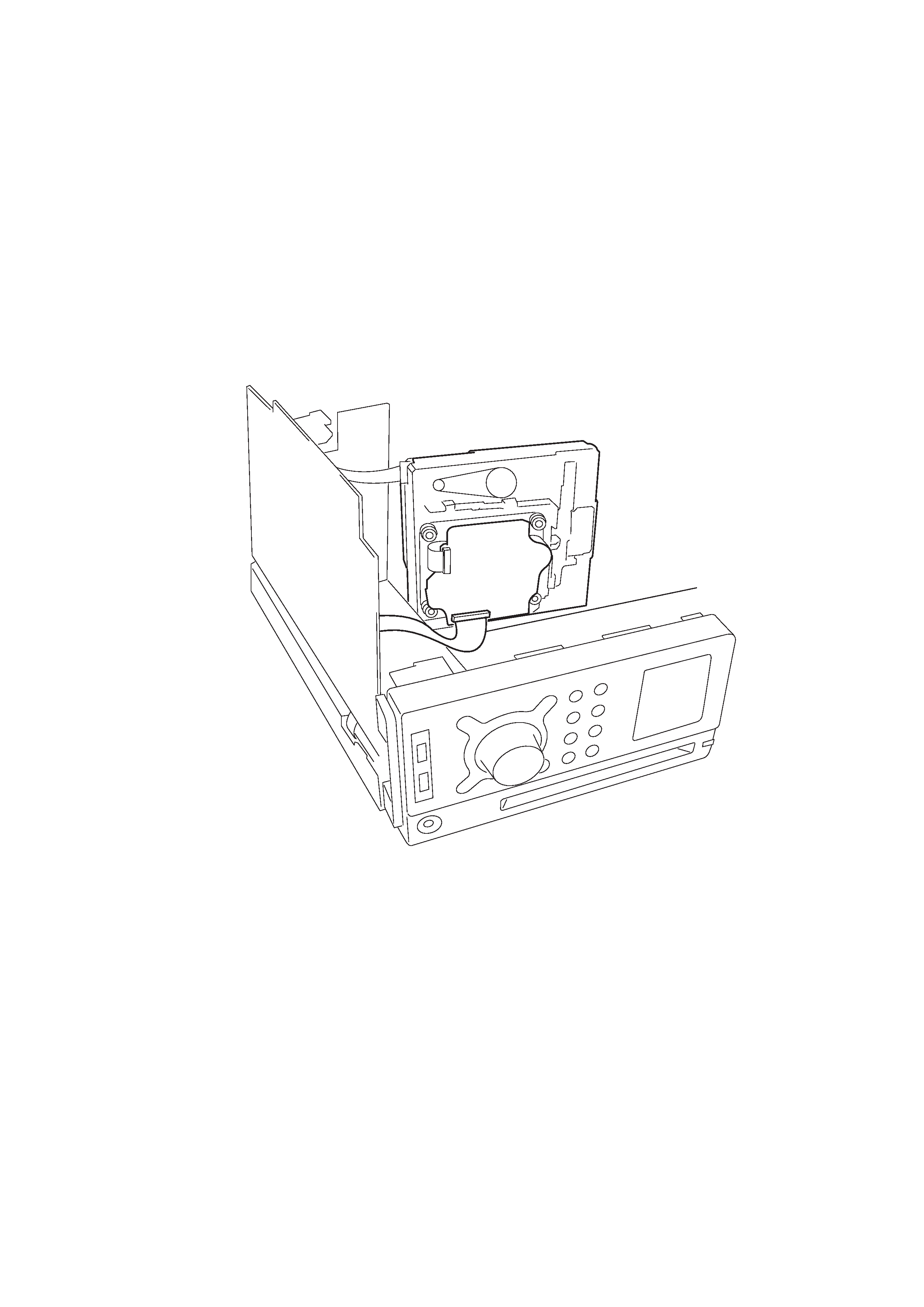
SERVICE POSITIONS
1-1. CDM SERVICE POSITION
·The CDM is specified in vertical position and this is the standard position.
Check signals such as RF waveform in this position.
· Extension of this flexible cable increases workability.
1mm pitch/27-pin/L300
Jig No.J-2501-214-A
J-2501-214-A
Ver 1.1