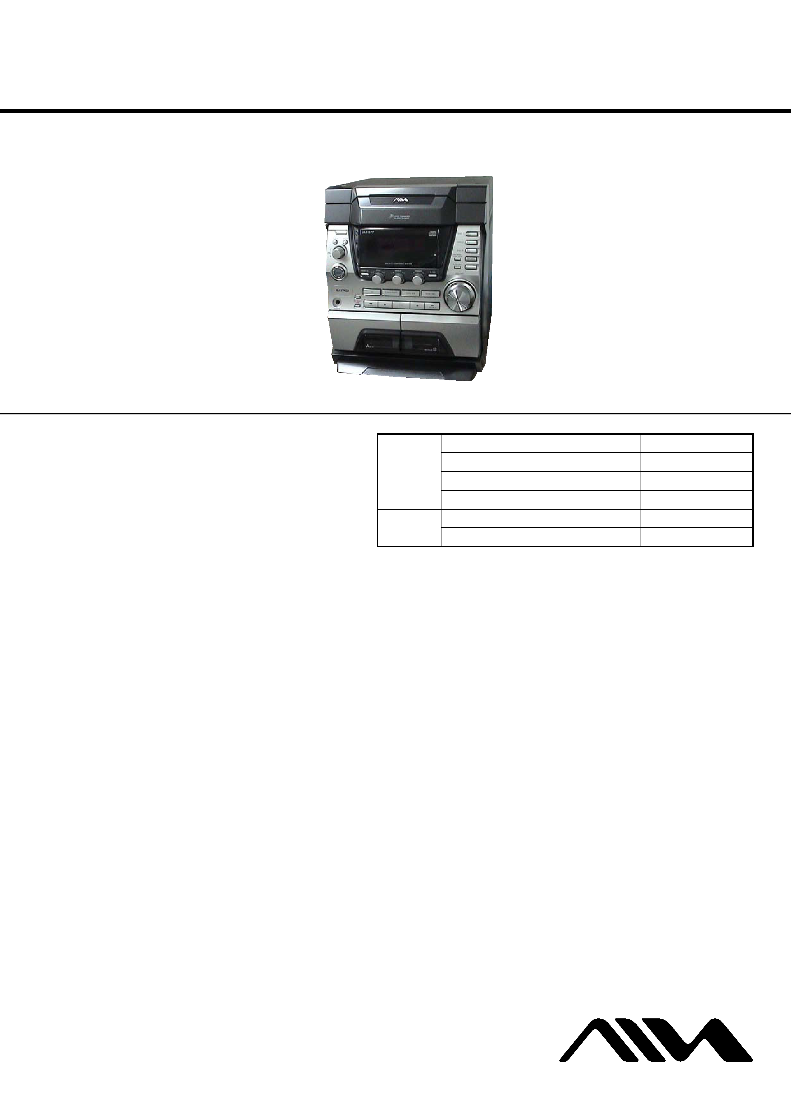
SERVICE MANUAL
COMPACT DISC DECK RECEIVER
US Model
Canadian Model
CX-JS77
Ver. 1.2 2005.05
9-877-747-03
Sony Corporation
2005E05-1
Personal Audio Group
© 2005.05
Published by Sony Engineering Corporation
SPECIFICATIONS
CX-JS77 is the amplifier, CD player, tape deck
and tuner section in JAX-S77.
Model Name Using Similar Mechanism
NEW
CD
CD Mechanism Type
CDM74-F1BD81
Section
Base Unit Name
BU-F1BD81A
Optical Pick-up Block Name
KSM-215DCP
Tape deck
Model Name Using Similar Mechanism
CX-JN5
Section
Tape Transport Mechanism Type
CWM43FF13
Amplifier section
AUDIO POWER SPECIFICATIONS
(USA models only)
POWER OUTPUT AND TOTAL HARMONIC
DISTORTION:
With 6 ohm loads, both channels driven, from
120 10,000 Hz: rated 180 watts per channel
minimum RMS power, with no more than 10%
total harmonic distortion from 250 milliwatts to
rated output.
Continuous RMS power output (reference):
180 + 180 watts (6 ohms at
1 kHz, 10% THD)
Total harmonic distortion less than 0.07% (6 ohms at
1kHz, 80 W)
Inputs
VIDEO/MD IN (phono jacks):
voltage 450/250 mV,
impedance 47 kilohms
Outputs
PHONES (stereo mini jack):
accepts headphones of
8 ohms or more
SPEAKER:
accepts impedance of 6 to
16 ohms
CD player section
System
Compact disc and digital
audio system
Laser
Semiconductor laser
(
=780 nm)
Emission duration:
continuous
Frequency response
2 Hz 20 kHz (
±0.5 dB)
Signal-to-noise ratio
More than 90 dB
Dynamic range
More than 90 dB
Tape deck section
Recording system
4-track 2-channel, stereo
Frequency response
50 13,000 Hz (
±3 dB),
using Sony TYPE I
cassettes
Tuner section
FM stereo, FM/AM superheterodyne tuner
FM tuner section
Tuning range
87.5 108.0 MHz
(100-kHz step)
Antenna
FM lead antenna
Antenna terminals
75 ohms unbalanced
Intermediate frequency
10.7 MHz
AM tuner section
Tuning range
530 1,710 kHz
(with the tuning interval
set at 10 kHz)
531 1,710 kHz
(with the tuning interval
set at 9 kHz)
Antenna
AM loop antenna
Antenna terminals
External antenna terminal
Intermediate frequency
450 kHz
General
Power requirements
120 V AC, 60 Hz
Power consumption
165 watts
Dimensions (w/h/d) incl. projecting parts and controls
Amplifier/Tuner/Tape/CD section:
Approx. 280
× 325 ×
425 mm
Mass
Approx. 9.9 kg
Design and specifications are subject to change
without notice.
CX-JS77
2
Notes on chip component replacement
· Never reuse a disconnected chip component.
· Notice that the minus side of a tantalum capacitor may be dam-
aged by heat.
Flexible Circuit Board Repairing
· Keep the temperature of the soldering iron around 270 °C dur-
ing repairing.
· Do not touch the soldering iron on the same conductor of the
circuit board (within 3 times).
· Be careful not to apply force on the conductor when soldering
or unsoldering.
CAUTION
Use of controls or adjustments or performance of procedures
other than those specified herein may result in hazardous ra-
diation exposure.
SAFETY-RELATED COMPONENT WARNING!!
COMPONENTS IDENTIFIED BY MARK 0 OR DOTTED
LINE WITH MARK 0 ON THE SCHEMATIC DIAGRAMS
AND IN THE PARTS LIST ARE CRITICAL TO SAFE
OPERATION. REPLACE THESE COMPONENTS WITH
SONY PARTS WHOSE PART NUMBERS APPEAR AS
SHOWN IN THIS MANUAL OR IN SUPPLEMENTS PUB-
LISHED BY SONY.
UNLEADED SOLDER
Boards requiring use of unleaded solder are printed with the lead-
free mark (LF) indicating the solder contains no lead.
(Caution: Some printed circuit boards may not come printed with
the lead free mark due to their particular size)
: LEAD FREE MARK
Unleaded solder has the following characteristics.
· Unleaded solder melts at a temperature about 40 °C higher than
ordinary solder.
Ordinary soldering irons can be used but the iron tip has to be
applied to the solder joint for a slightly longer time.
Soldering irons using a temperature regulator should be set to
about 350
°C.
Caution: The printed pattern (copper foil) may peel away if the
heated tip is applied for too long, so be careful!
· Strong viscosity
Unleaded solder is more viscou-s (sticky, less prone to flow)
than ordinary solder so use caution not to let solder bridges oc-
cur such as on IC pins, etc.
· Usable with ordinary solder
It is best to use only unleaded solder but unleaded solder may
also be added to ordinary solder.
SAFETY CHECK-OUT
After correcting the original service problem, perform the follow-
ing safety check before releasing the set to the customer:
Check the antenna terminals, metal trim, "metallized" knobs,
screws, and all other exposed metal parts for AC leakage.
Check leakage as described below.
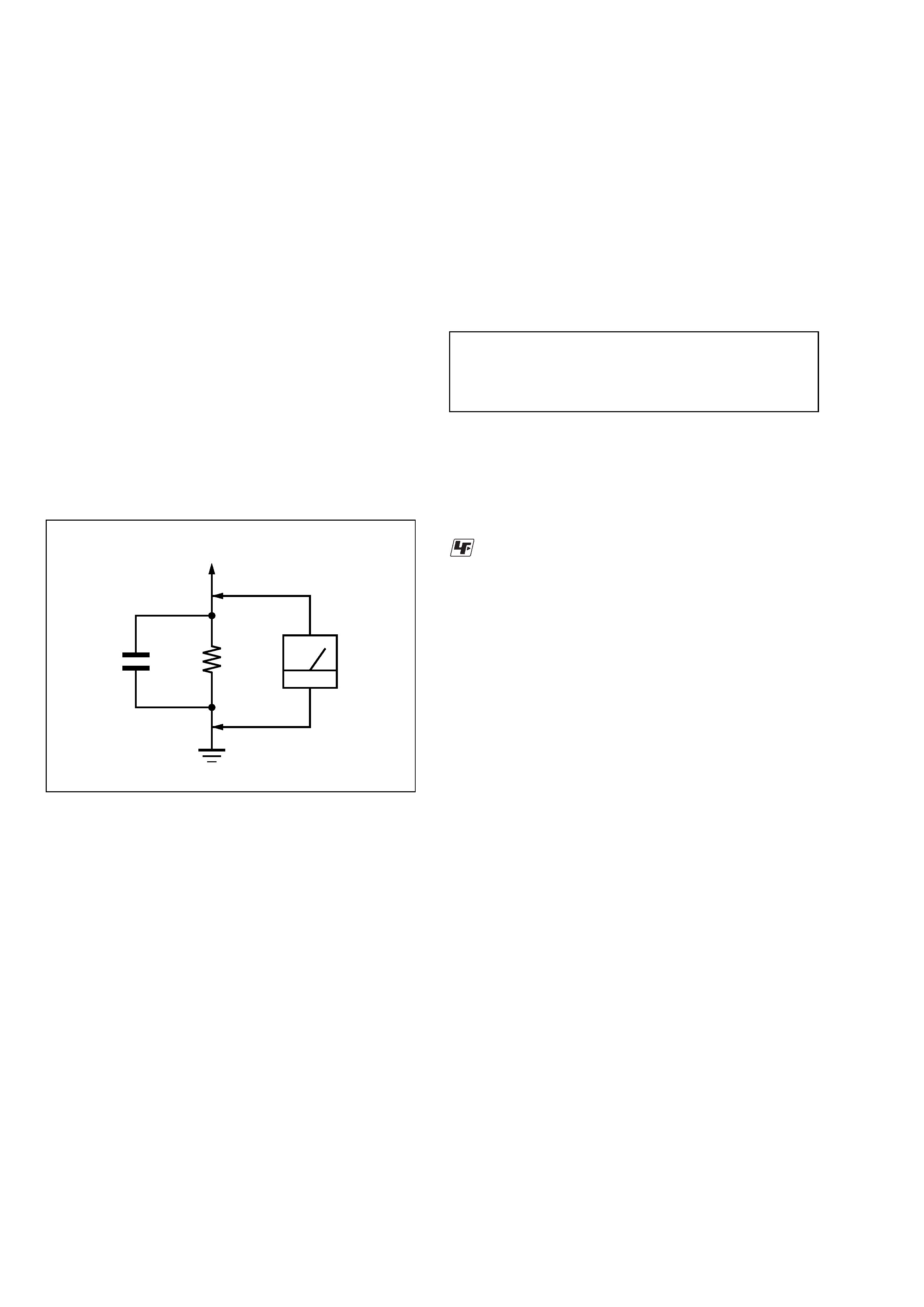
LEAKAGE TEST
The AC leakage from any exposed metal part to earth ground and
from all exposed metal parts to any exposed metal part having a
return to chassis, must not exceed 0.5 mA (500 microamperes.).
Leakage current can be measured by any one of three methods.
1. A commercial leakage tester, such as the Simpson 229 or RCA
WT-540A. Follow the manufacturers' instructions to use these
instruments.
2. A battery-operated AC milliammeter. The Data Precision 245
digital multimeter is suitable for this job.
3. Measuring the voltage drop across a resistor by means of a
VOM or battery-operated AC voltmeter. The "limit" indica-
tion is 0.75 V, so analog meters must have an accurate low-
voltage scale. The Simpson 250 and Sanwa SH-63Trd are ex-
amples of a passive VOM that is suitable. Nearly all battery
operated digital multimeters that have a 2 V AC range are suit-
able. (See Fig. A)
Fig. A.
Using an AC voltmeter to check AC leakage.
1.5 k
0.15
µF
AC
voltmeter
(0.75 V)
To Exposed Metal
Parts on Set
Earth Ground
ATTENTION AU COMPOSANT AYANT RAPPORT
À LA SÉCURITÉ!
LES COMPOSANTS IDENTIFIÉS PAR UNE MARQUE 0
SUR LES DIAGRAMMES SCHÉMATIQUES ET LA LISTE
DES PIÈCES SONT CRITIQUES POUR LA SÉCURITÉ
DE FONCTIONNEMENT. NE REMPLACER CES COM-
POSANTS QUE PAR DES PIÈCES SONY DONT LES
NUMÉROS SONT DONNÉS DANS CE MANUEL OU
DANS LES SUPPLÉMENTS PUBLIÉS PAR SONY.

CX-JS77
3
TABLE OF CONTENTS
1.
SERVICING NOTES ................................................ 4
2.
GENERAL
Location of Controls .......................................................
7
Setting the Clock .............................................................
8
3.
DISASSEMBLY
3-1. Disassembly Flow ...........................................................
9
3-2. Case (Side-L/R) ............................................................... 10
3-3. Case (Top) ....................................................................... 10
3-4. Tray Panel ........................................................................ 11
3-5. CD Mechanism Deck (CDM74-F1BD81) ...................... 11
3-6. Front Panel Block ............................................................ 12
3-7. Back Panel Section .......................................................... 12
3-8. MAIN Board ................................................................... 13
3-9. Tape Mechanism Deck (CWM43FF13) ......................... 13
3-10. Table Assy ....................................................................... 14
3-11. MOTOR (TB) Board ....................................................... 14
3-12. MOTOR (LD) Board ....................................................... 15
3-13. Base Unit (BU-F1BD81A) ............................................. 15
3-14. CD Board ......................................................................... 16
4.
TEST MODE .............................................................. 17
5.
ELECTRICAL ADJUSTMENTS
CD Section ...................................................................... 21
6.
DIAGRAMS
6-1. Block Diagram SERVO Section .............................. 22
6-2. Block Diagram MAIN Section ................................ 23
6-3. Block Diagram
PANEL/POWER SUPPLY Section .......................... 24
6-4. Note for Printed Wiring Boards and
Schematic Diagrams ....................................................... 25
6-5. Printed Wiring Board CD Board ............................. 26
6-6. Schematic Diagram CD Board ................................ 27
6-7. Printed Wiring Boards CHANGER Section ............ 28
6-8. Schematic Diagram CHANGER Section ................ 29
6-9. Printed Wiring Board
CDMP3 CONNECT Board ...................................... 30
6-10. Schematic Diagram
CDMP3 CONNECT Board ...................................... 31
6-11. Schematic Diagram MAIN Section (1/4) ................ 32
6-12. Schematic Diagram MAIN Section (2/4) ................ 33
6-13. Schematic Diagram MAIN Section (3/4) ................ 34
6-14. Schematic Diagram MAIN Section (4/4) ................ 35
6-15. Printed Wiring Boards MAIN Section .................... 36
6-16. Printed Wiring Board PANEL Section .................... 37
6-17. Schematic Diagram PANEL Section (1/2) .............. 38
6-18. Schematic Diagram PANEL Section (2/2) .............. 39
6-19. Printed Wiring Board POWER AMP Section ......... 40
6-20. Schematic Diagram POWER AMP Section ............ 41
6-21. Printed Wiring Boards TRANS Section .................. 42
6-22. Schematic Diagram TRANS Section ...................... 43
7.
EXPLODED VIEWS
7-1. Case Section .................................................................... 54
7-2. Tape Mechanism Deck Section (CWM43FF13) ............ 55
7-3. Cassette Box Section ...................................................... 56
7-4. Front Panel Section ......................................................... 57
7-5. Back Panel Section .......................................................... 58
7-6. Chassis Section ............................................................... 59
7-7. CD Mechanism Deck Section-1 (CDM74-F1BD81) ..... 60
7-8. CD Mechanism Deck Section-2 (CDM74-F1BD81) ..... 61
7-9. CD Mechanism Deck Section-3 (CDM74-F1BD81) ..... 62
7-10. Base Unit Section (BU-F1BD81A) ................................ 63
8.
ELECTRICAL PARTS LIST ............................... 64

4
CX-JS77
SECTION 1
SERVICING NOTES
NOTES ON HANDLING THE OPTICAL PICK-UP
BLOCK OR BASE UNIT
The laser diode in the optical pick-up block may suffer electro-
static break-down because of the potential difference generated
by the charged electrostatic load, etc. on clothing and the human
body.
During repair, pay attention to electrostatic break-down and also
use the procedure in the printed matter which is included in the
repair parts.
The flexible board is easily damaged and should be handled with
care.
NOTES ON LASER DIODE EMISSION CHECK
The laser beam on this model is concentrated so as to be focused
on the disc reflective surface by the objective lens in the optical
pick-up block. Therefore, when checking the laser diode emis-
sion, observe from more than 30 cm away from the objective lens.
LASER DIODE AND FOCUS SEARCH OPERATION
CHECK
Carry out the "S curve check" in "CD section adjustment" and
check that the S curve waveforms is output three times.
5
CX-JS77
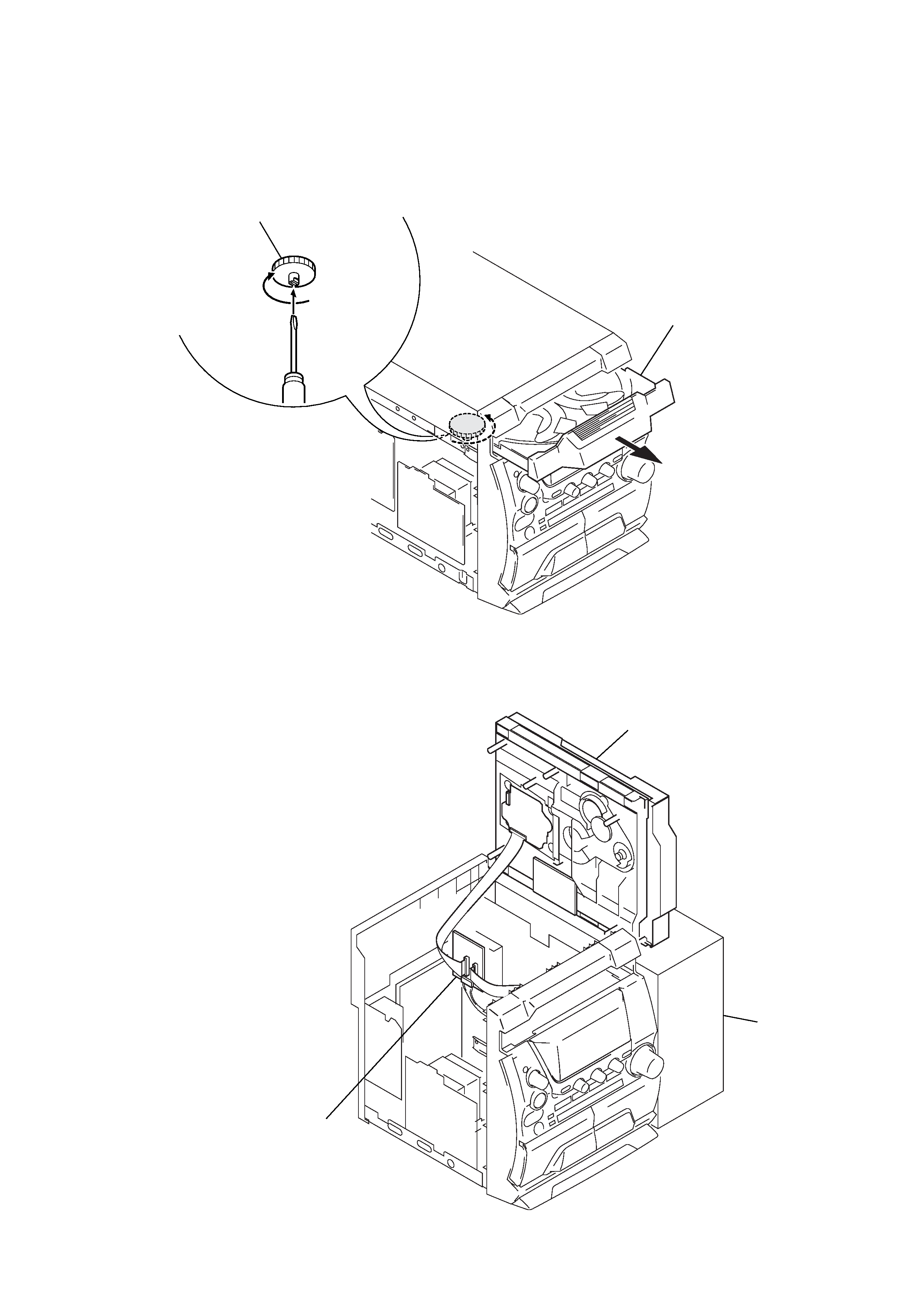
SERVICE POSITION
CD MECHANISM DECK
HOW TO OPEN THE DISC TRAY WHEN POWER SWITCH TURNS OFF.
1
Remove the case (side-L).
2
Turn the loading gear in the direction
of arrow A.
A
3
Pull-out the disc tray.
CD mechanism deck
stand
CDMP3 CONNECT board