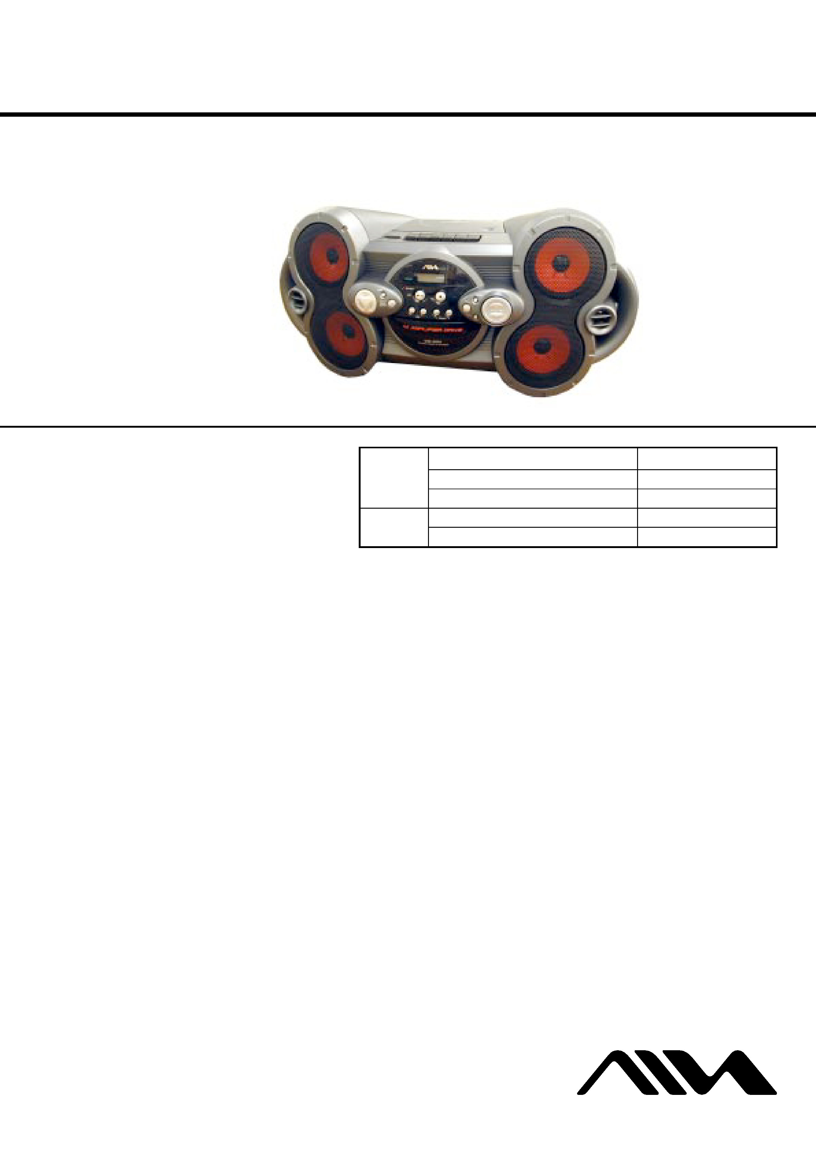
CSD-XD51
US Model
SERVICE MANUAL
CD STEREO RADIO CASSETTE RECORDER
Sony Corporation
Personal Audio Company
Published by Sony Engineering Corporation
9-877-952-01
2004F0279-1
© 2004.06
SPECIFICATIONS
Ver 1.0 2004. 06
Continued on next page
CD
Model Name Using Similar Mechanism
CSD-XD55
Section
CD Mechanism Type
KSM-213RDP
Optical Pick-up Name
KSS-213R
TC
Model Name Using Similar Mechanism
CSD-XD55
Section
Tape Transport Mechanism Type
MF-XD55
AUDIO POWER SPECIFICATIONS
POWER OUTPUT AND TOTAL
HARMONIC DISTORTION
With 3.2-ohm loads, both channels driven from 150 - 6,300 Hz;
rated 3.0 W per channel-minimum RMS power, with no more than
10 % total harmonic distortion in AC operation.
Other specifications
CD player section
System
Compact disc digital audio system
Laser diode properties
Material: GaAlAs
Wave length: 780 nm
Emission duration: Continuous
Laser output: Less than 44.6
µW
(This output is the value measured at a distance of about
200 mm from the objective lens surface on the optical
pick-up block with 7 mm aperture.)
Spindle speed
200 r/min (rpm) to 500 r/min (rpm)
(CLV)
Number of channels
2
Frequency response
20 - 20 000 Hz +1/2 dB
Wow and flutter
Below measurable limit
Radio section
Frequency range
FM
87.5 - 108 MHz
AM
530 - 1 710 kHz
Antennas
FM: Telescopic antenna
AM: Built-in ferrite bar antenna
Cassette recorder section
Recording system
4-track 2 channel stereo
Fast winding time
Approx. 120 s (sec.) with Sony cassette C-60
Frequency response
TYPE I (normal): 80 - 10 000 Hz
General
Speaker
Full range: 10 cm dia., 3.2 ohms, cone type (4)
Tweeter: 2.0 cm (2)
Outputs
Headphones jack (stereo minijack)
For 16 - 68 ohms impedance headphones
2
CSD-XD51
Power output
4.5 W + 4.5 W (at 3.2 ohms, 10% harmonic distortion
(DC))
Power requirements
For CD stereo radio cassette recorder:
120V AC, 60 Hz
9 V DC, 6 size D (R20) batteries
Power consumption
AC 17 W
Battery life
For CD stereo radio cassette recorder:
FM recording
Sony R20P: approx. 12 h
Sony alkaline LR20: approx. 34 h
Tape playback
Sony R20P: approx. 5.5 Ah
Sony alkaline LR20: approx. 15.5 h
CD playback
Sony R20P: approx. 2.5 h
Sony alkaline LR20: approx. 12 h
Dimensions
Approx. 552 x 271 x 318 mm (w/h/d)
(21 3/
4 x 10
5/
8 x12
1/
2 inches) (incl. projecting parts)
Mass
Approx. 5.4 kg (11 lb. 14 oz) (incl. batteries)
Supplied accessory
AC power cord (1)
Design and specifications are subject to changewithout notice.
CAUTION
Use of controls or adjustments or performance of procedures
other than those specified herein may result in hazardous
radiation exposure.
Flexible Circuit Board Repairing
· Keep the temperature of soldering iron around 270°C
during repairing.
· Do not touch the soldering iron on the same conductor of the
circuit board (within 3 times).
· Be careful not to apply force on the conductor when soldering
or unsoldering.
Notes on chip component replacement
· Never reuse a disconnected chip component.
· Notice that the minus side of a tantalum capacitor may be
damaged by heat.
NOTES ON HANDLING THE OPTICAL PICK-UP BLOCK
OR BASE UNIT
The laser diode in the optical pick-up block may suffer electrostatic
break-down because of the potential difference generated by the
charged electrostatic load, etc. on clothing and the human body.
During repair, pay attention to electrostatic break-down and also
use the procedure in the printed matter which is included in the
repair parts.
The flexible board is easily damaged and should be handled with
care.
NOTES ON LASER DIODE EMISSION CHECK
The laser beam on this model is concentrated so as to be focused on
the disc reflective surface by the objective lens in the optical pick-
up block. Therefore, when checking the laser diode emission,
observe from more than 30 cm away from the objective lens.
After correcting the original service problem, perform the following
safety checks before releasing the set to the customer:
Check the antenna terminals, metal trim, "metallized" knobs, screws,
and all other exposed metal parts for AC leakage. Check leakage as
described below.
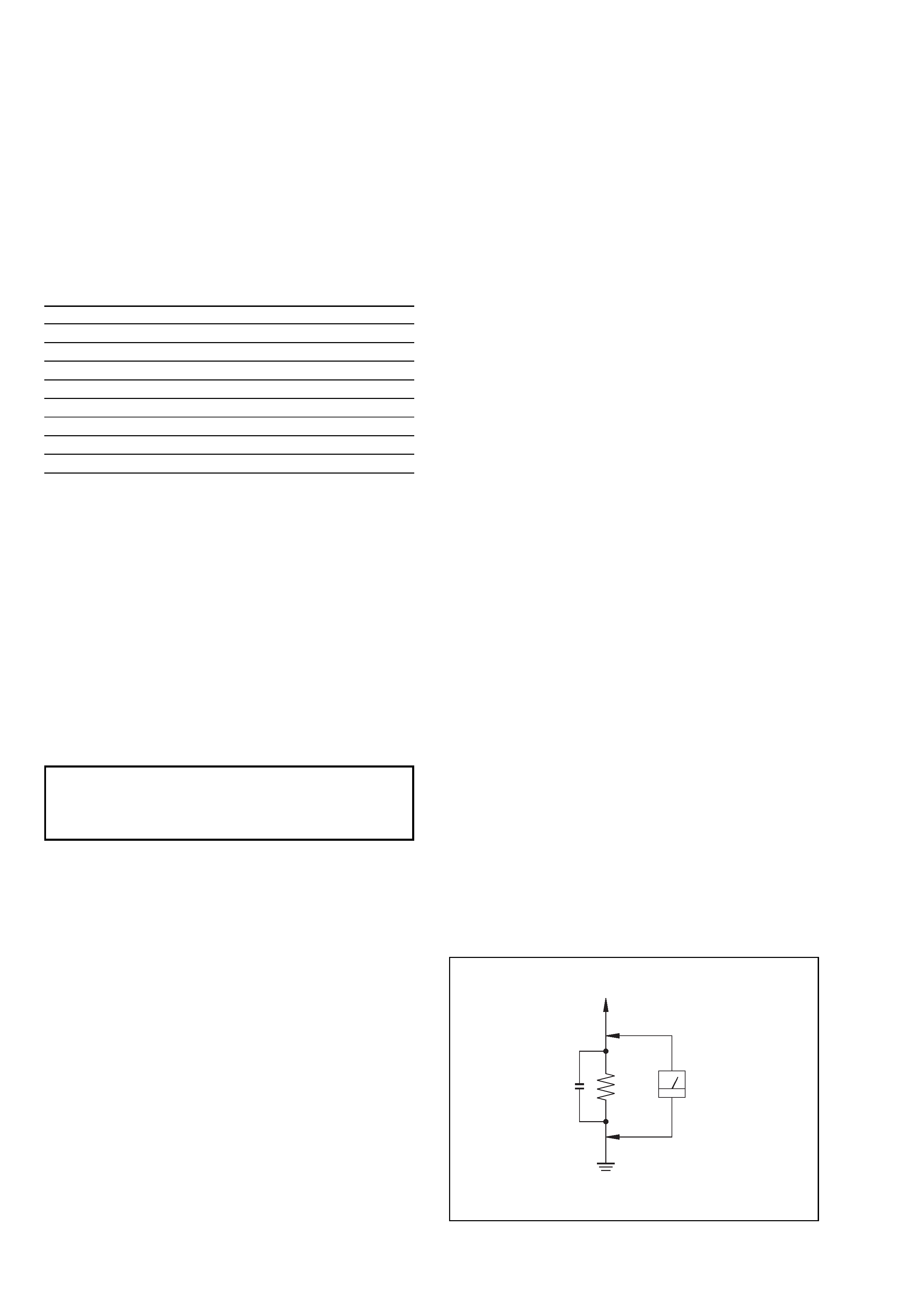
LEAKAGE
The AC leakage from any exposed metal part to earth ground and
from all exposed metal parts to any exposed metal part having a
return to chassis, must not exceed 0.5 mA (500 microamperes).
Leakage current can be measured by any one of three methods.
1. A commercial leakage tester, such as the Simpson 229 or RCA
WT-540A. Follow the manufacturers' instructions to use these
instruments.
2. A battery-operated AC milliammeter. The Data Precision 245
digital multimeter is suitable for this job.
3. Measuring the voltage drop across a resistor by means of a
VOM or battery-operated AC voltmeter. The "limit" indication
is 0.75 V, so analog meters must have an accurate low-voltage
scale. The Simpson 250 and Sanwa SH-63Trd are examples
of a passive VOM that is suitable. Nearly all battery operated
digital multimeters that have a 2V AC range are suitable. (See
Fig. A)
SAFETY CHECK-OUT
To Exposed Metal
Parts on Set
0.15 µF
1.5 k
AC
Voltmeter
(0.75 V)
Earth Ground
Fig. A. Using an AC voltmeter to check AC leakage.

3
CSD-XD51
Unleaded solder
Boards requiring use of unleaded solder are printed with the lead-
free mark (LF) indicating the solder contains no lead.
(Caution: Some printed circuit boards may not come printed with
the lead free mark due to their particular size.)
: LEAD FREE MARK
Unleaded solder has the following characteristics.
·Unleaded solder melts at a temperature about 40
°C higher than
ordinary solder.
Ordinary soldering irons can be used but the iron tip has to be
applied to the solder joint for a slightly longer time.
Soldering irons using a temperature regulator should be set to
about 350
°C.
Caution: The printed pattern (copper foil) may peel away if
the heated tip is applied for too long, so be careful!
· Strong viscosity
Unleaded solder is more viscous (sticky, less prone to flow)
than ordinary solder so use caution not to let solder bridges
occur such as on IC pins, etc.
· Usable with ordinary solder
It is best to use only unleaded solder but unleaded solder may
also be added to ordinary solder.
Note on chip component replacement
· Never reuse a disconnected chip component.
· Notice that the minus side of a tantalum capacitor may be
damaged by heat.
SAFETY-RELATED COMPONENT WARNING!!
COMPONENTS IDENTIFIED BY MARK 0 OR DOTTED LINE WITH
MARK 0 ON THE SCHEMATIC DIAGRAMS AND IN THE PARTS
LIST ARE CRITICAL TO SAFE OPERATION. REPLACE THESE
COMPONENTS WITH SONY PARTS WHOSE PART NUMBERS
APPEAR AS SHOWN IN THIS MANUAL OR IN SUPPLEMENTS
PUBLISHED BY SONY.
TABLE OF CONTENTS
1.
SERVICING NOTES ................................................ 4
2.
GENERAL ................................................................... 5
3.
DISASSEMBLY
3-1.
Disassembly Flow ........................................................... 6
3-2.
Cabinet (Top) Assy .......................................................... 6
3-3.
Cabinet (Front Assy), Cabinet (Bottom) Assy ................. 7
3-4.
Wires ................................................................................ 8
3-5.
MD Block ........................................................................ 9
3-6.
Cassette Holder ................................................................ 9
3-7.
Main Board ...................................................................... 10
3-8.
Tuner Board ..................................................................... 10
3-9.
Power Board .................................................................... 11
3-10. CD Lid ............................................................................. 11
3-11. CD Block Assy ................................................................ 12
3-12. Optical Pick-up ................................................................ 12
3-13. R/P Head (HRP301), TC Board ...................................... 13
3-14. Main Belt, RF Belt, Motor Assy (M301) ........................ 13
4.
MECHANICAL ADJUSTMENTS ......................... 14
5.
ELECTRICAL ADJUSTMENTS .......................... 14
6.
DIAGRAMS
6-1.
IC Pin Description ........................................................... 17
6-2.
Circuit Boards Location .................................................. 17
6-3.
Block Diagram CD Section ....................................... 18
6-4.
Block Diagram Main Section .................................... 19
6-5.
Printed Wiring Board CD Section ............................. 20
6-6.
Schematic Diagram CD Section ................................ 21
6-7.
Printed Wiring Board Tuner Section ......................... 22
6-8.
Schematic Diagram Tuner Section ............................ 23
6-9.
Printed Wiring Board Main Section .......................... 24
6-10. Schematic Diagram Main Section (1/2) .................... 25
6-11. Schematic Diagram Main Section (2/2) .................... 26
6-12. Printed Wiring Board TC Section .............................. 27
6-13. Schematic Diagram TC Section ................................ 28
6-14. Printed Wiring Board Control Section ...................... 29
6-15. Schematic Diagram Control Section ......................... 30
6-16. Printed Wiring Board Power Supply Section ............ 31
6-17. Schematic Diagram Power Supply Section ............... 32
6-18. IC Block Diagrams .......................................................... 33
7.
EXPLODED VIEWS
7-1.
Cabinet Section ................................................................ 36
7-2.
Cabinet (Front) Section-1 ................................................ 37
7-3.
Cabinet (Front) Section-2 ................................................ 38
7-4.
Cabinet (Top) Section ...................................................... 39
7-5.
Cabinet (Bottom) Section ................................................ 40
7-6.
Tape Mechanism Section (MF-XD55) ............................ 41
7-7.
CD Mechanism Section (KSM-213RDP) ....................... 42
8.
ELECTRICAL PARTS LIST .................................. 43
4
CSD-XD51
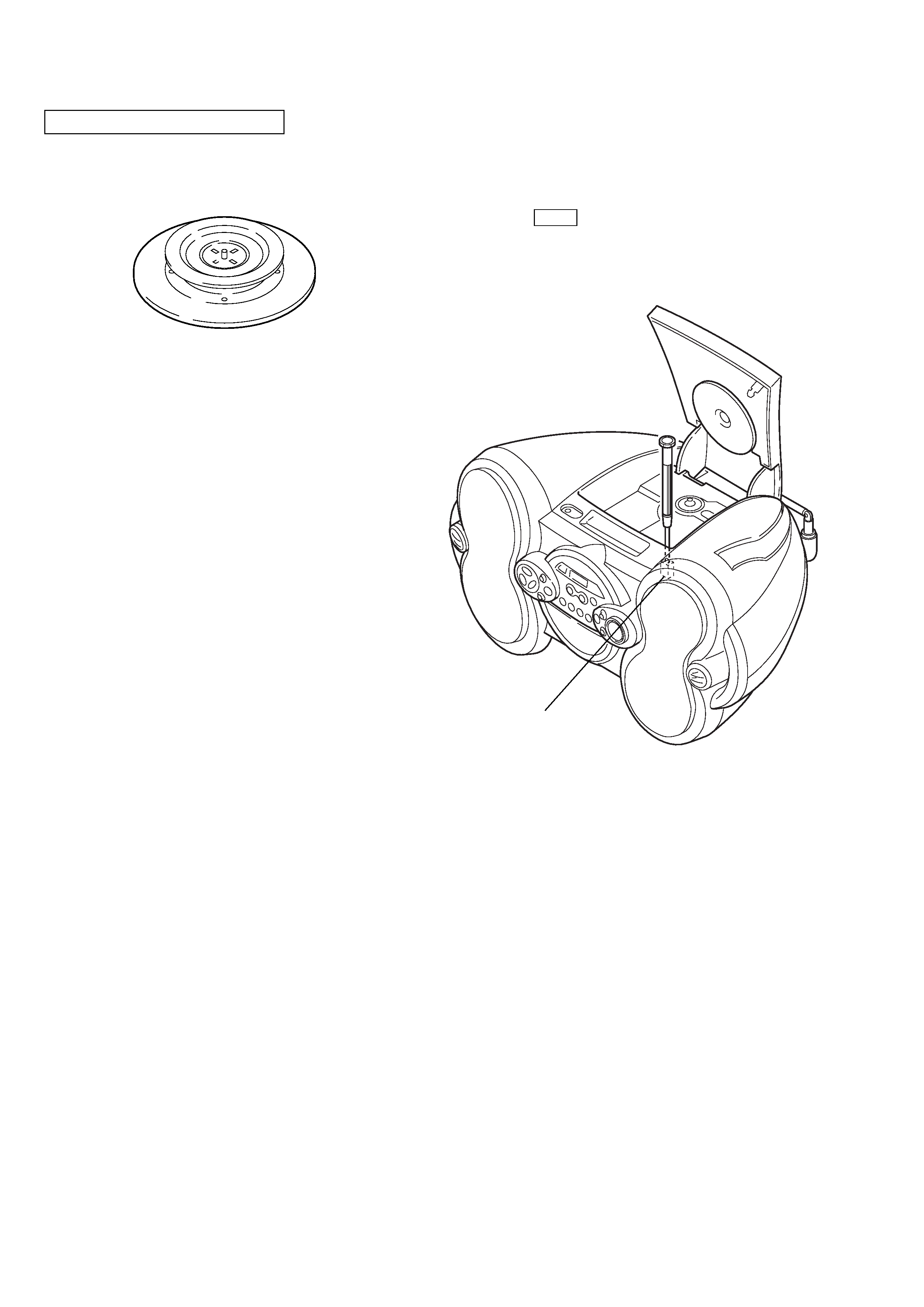
CHUCK PLATE JIG ON REPAIRING
SECTION 1
SERVICING NOTES
LASER DIODE AND FOCUS SEARCH OPERATION
CHECK
1.
Turn ON the[OPERATE]button and press[CD] button to CD
position.
2.
Open the CD lid.
3.
Turn on S801 with screwdriver, etc. as following figure.
4.
Press the N X (CD) button.
5.
Confirm the laser diode emission while observing the objecting
lens. When there is no emission, Auto Power Control circuit
or Optical Pick-up is broken.
Objective lens moves up and down three times for focus search.
S801
On repairing CD section, playing a disc without the lid (CD), use
Chuck Plate Jig.
· Code number of Chuck Plate Jig: X-4918-255-1
5
CSD-XD51
SECTION 2
GENERAL
This section is extracted
from instruction manual.
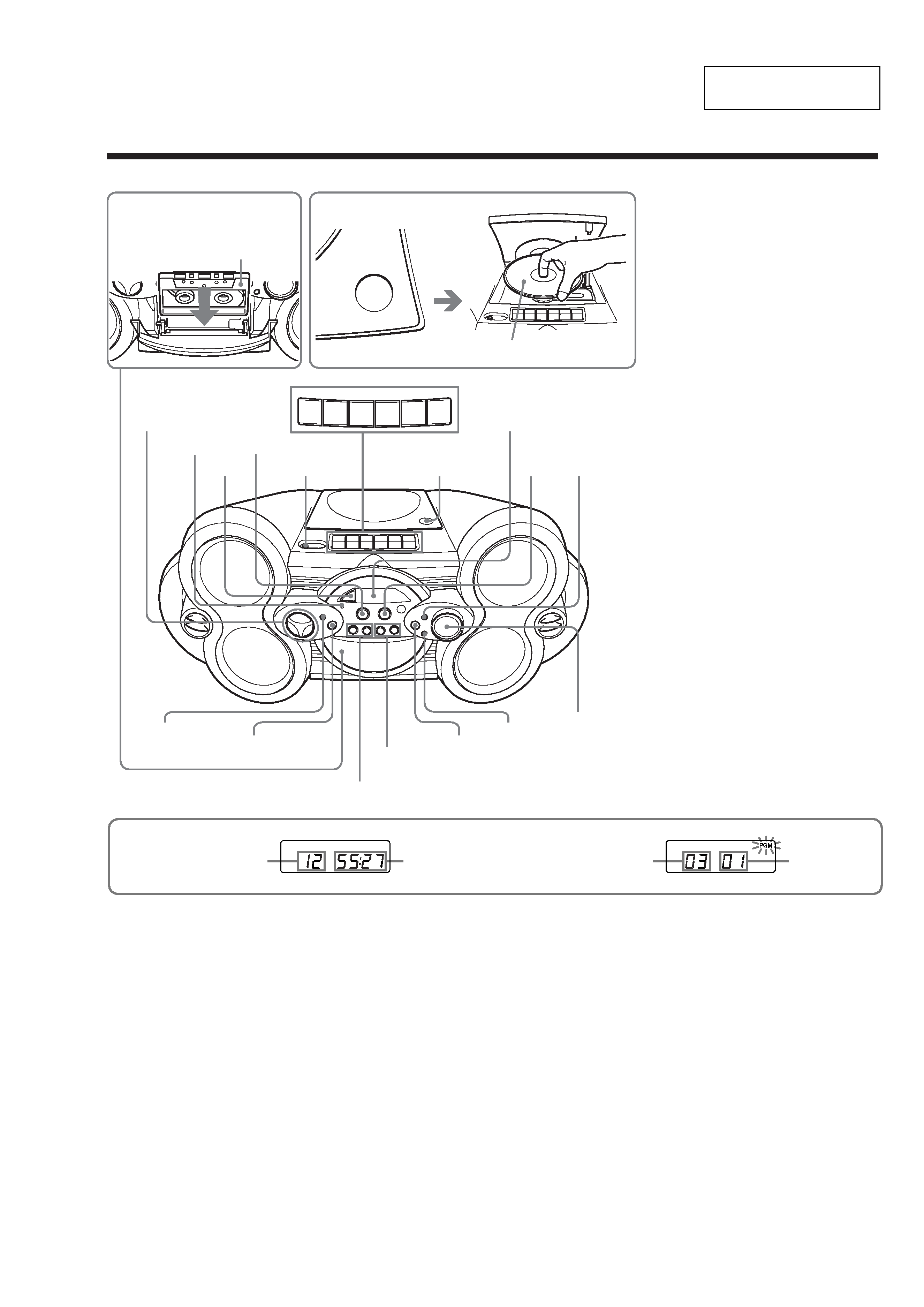
LOCATING THE CONTROLS
Location of controls
ZPUSH
OPEN/CLOSE
PAUSE STOP/EJECT
FF
REW
PLAY
REC
TUNE ,+
VOLUME ,+*
ZPUSH OPEN/CLOSE
SURROUND
S-BASS
SLEEP
u
POWER
HEADPHONES
OPR/BATT
MODE
DISPLAY/ENTER/MEMORY
.,>
PRESET ,+
CD, RADIO BAND/
AUTO PRESET, TAPE
x
Loading a CD
With the labeled side up
Inserting a cassette
With the side you want
to play facing you
Total track number
Programmed track
Playing order
EF
Total playing time
Display
*The button has a tactile dot.
Display