1
Ver 1.1 2001. 02
Model Name Using Similar Mechanism
CDX-CA650
CD Drive Mechanism Type
MG-393X-121//Q
Optical Pick-up Name
KSS-720A
SERVICE MANUAL
AEP Model
UK Model
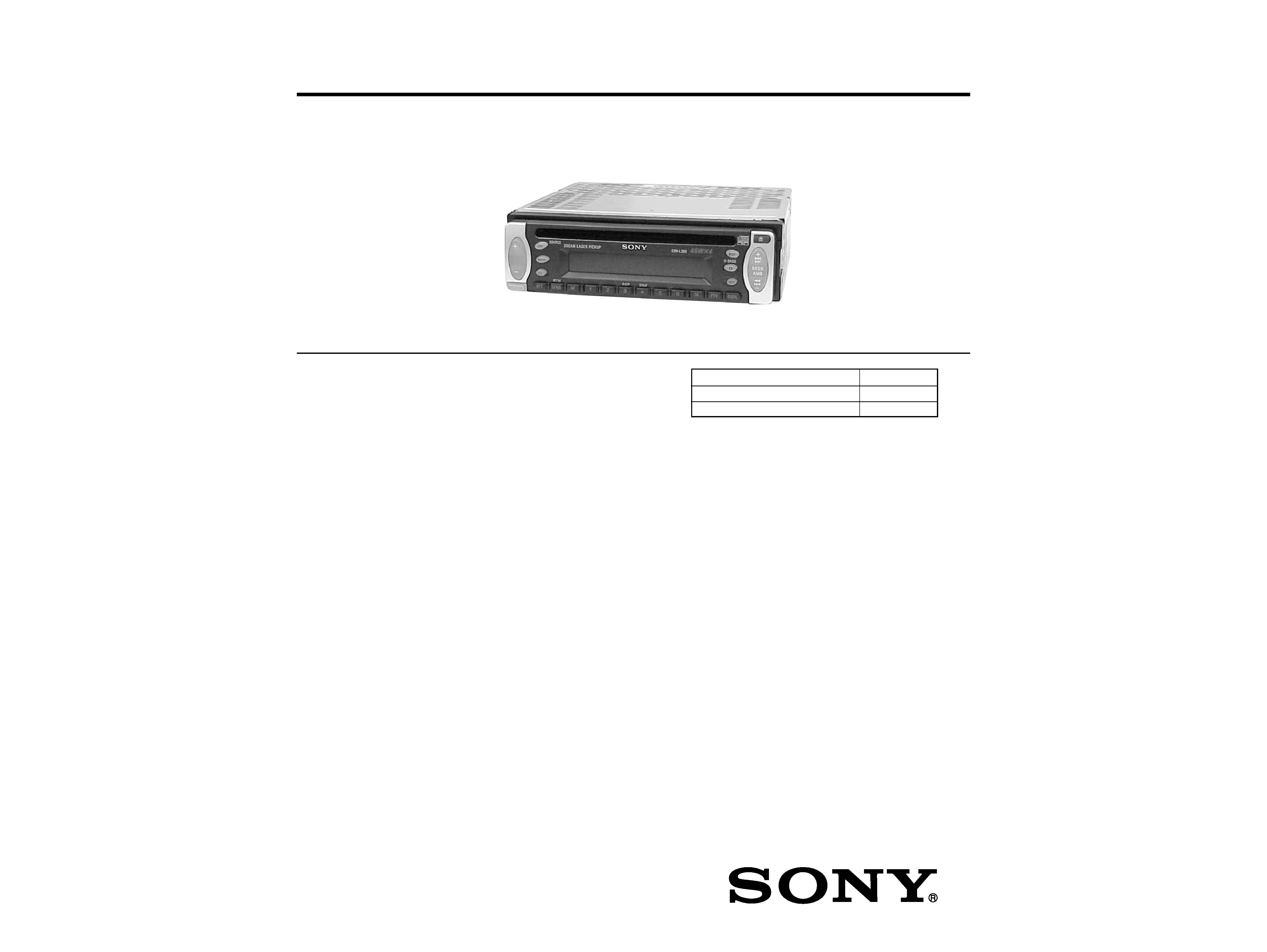
CDX-L350/L360
E Model
CDX-L350
CDX-L350/L360
FM/MW/LW COMPACT DISC PLAYER
CD player section
Signal-to-noise ratio
90 dB
Frequency response
10 20,000 Hz
Wow and flutter
Below measurable limit
Tuner section
FM
Tuning range
87.5 108.0 MHz
Aerial terminal
External aerial connector
Intermediate frequency 10.7 MHz/450 kHz
Usable sensitivity
8 dBf
Selectivity
75 dB at 400 kHz
Signal-to-noise ratio
66 dB (stereo),
72 dB (mono)
Harmonic distortion at 1 kHz
0.6% (stereo),
0.3% (mono)
Separation
35 dB at 1 kHz
Frequency response
30 15,000 Hz
MW/LW
Tuning range
MW: 531 1,602 kHz
LW: 153 279 kHz
Aerial terminal
External aerial connector
Intermediate frequency 10.7 MHz/450 kHz
Sensitivity
MW: 30 µV
LW: 40 µV
Power amplifier section
Outputs
Speaker outputs
(sure seal connectors)
Speaker impedance
4 8 ohms
Maximum power output 45 W
× 4 (at 4 ohms)
SPECIFICATIONS
General
Outputs
Power aerial relay control
lead
Inputs
Telephone ATT control lead
Tone controls
Bass ±9 dB at 100 Hz
Treble ±9 dB at 10 kHz
Power requirements
12 V DC car battery
(negative ground)
Dimensions
Approx. 178
× 50 × 177 mm
(w/h/d)
Mounting dimension
Approx. 182
× 53 × 162 mm
(w/h/d)
Mass
Approx. 1.2 kg
Supplied accessories
Parts for installation and
connections (1 set)
Front panel case (1)
Design and specifications are subject to change without
notice.
Photo: CDX-L350
· The tuner and CD sections have no adjustments.
Sony Corporation
Audio Entertainment Group
General Engineering Dept.
9-870-278-12
2001B0400-1
© 2001. 2
2
TABLE OF CONTENTS
1. GENERAL
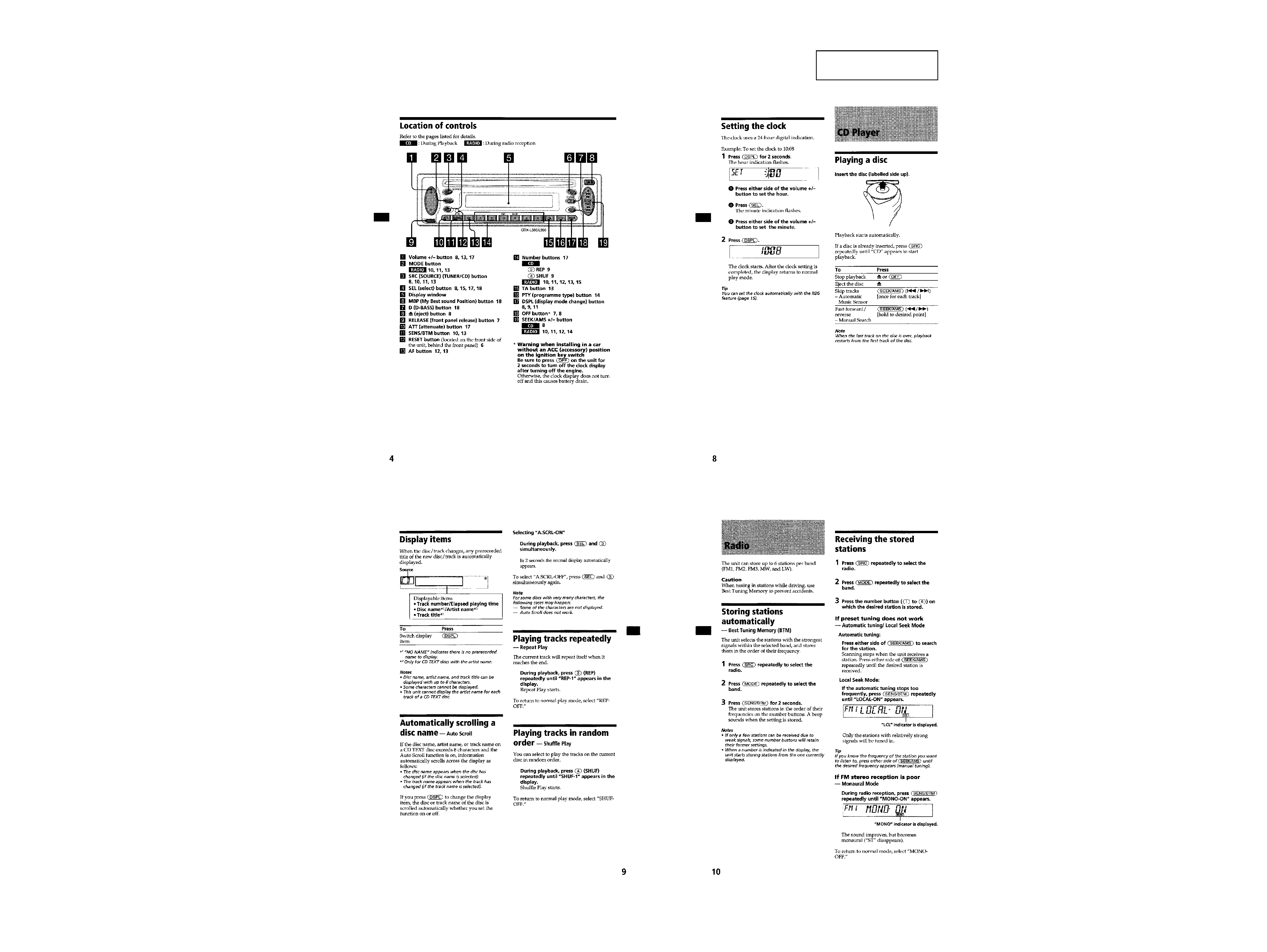
Location of Controls ................................................................ 3
Setting the Clock ..................................................................... 3
CD Player ................................................................................ 3
Radio ....................................................................................... 3
RDS ......................................................................................... 4
Other Functions ....................................................................... 5
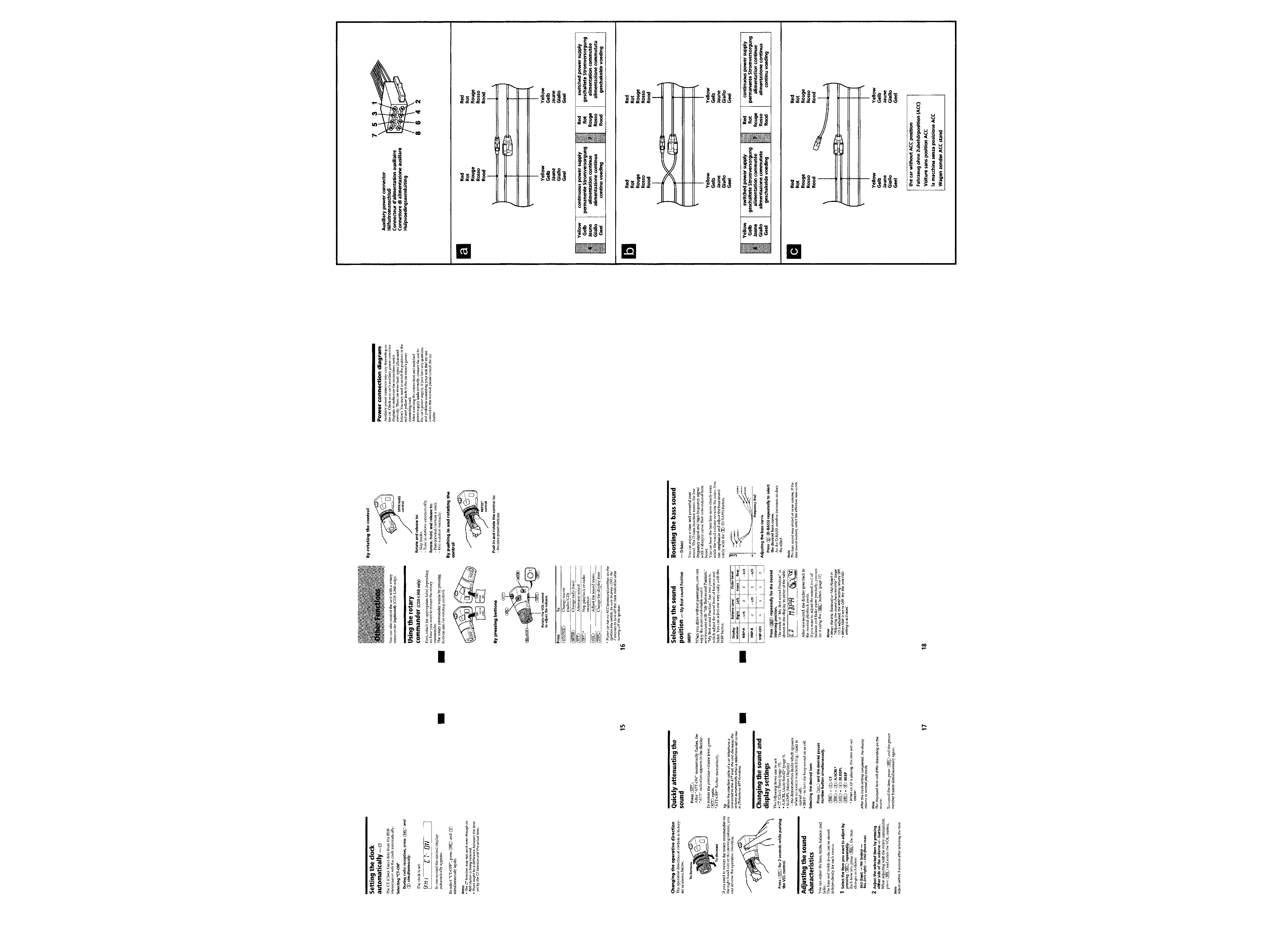
Connections ............................................................................. 5
2. DISASSEMBLY
2-1. Sub Panel Assy .................................................................... 7
2-2. CD Mechanism Block ......................................................... 8
2-3. Main Board ......................................................................... 8
2-4. Heat Sink ............................................................................. 9
2-5. Chassis (T.U) Assy .............................................................. 9
2-6. Disc In Board .................................................................... 10
2-7. Servo Board ....................................................................... 10
2-8. Arm Roller Assy ................................................................ 11
2-9. Chassis (OP) Assy ............................................................. 11
2-10. Optical Pick-up Block ....................................................... 12
3. DIAGRAMS
3-1. IC Pin Description ............................................................. 13
3-2. Block Diagram CD Section ........................................... 15
3-3. Block Diagram Tuner Section ....................................... 16
3-4. Block Diagram Display Section .................................... 17
3-5. Circuit Boards Location .................................................... 17
3-6. Printed Wiring Boards CD Mechanism Section ............ 18
3-7. Schematic Diagram CD Mechanism Section ................ 20
3-8. Printed Wiring Board Main Section .............................. 21
3-9. Schematic Diagram Main Section (1/2) ........................ 22
3-10. Schematic Diagram Main Section (2/2) ........................ 23
3-11. Printed Wiring Board Key Section ................................ 24
3-12. Schematic Diagram Key Section .................................. 25
4. EXPLODED VIEWS
4-1. Chassis Section ................................................................. 28
4-2. Front Panel Section ........................................................... 29
4-3. CD Mechanism Section (1) ............................................... 30
4-4. CD Mechanism Section (2) ............................................... 31
4-5. CD Mechanism Section (3) ............................................... 32
5. ELECTRICAL PARTS LIST ........................................ 33
SAFETY-RELATED COMPONENT WARNING!!
COMPONENTS IDENTIFIED BY MARK 0 OR DOTTED LINE
WITH MARK 0 ON THE SCHEMATIC DIAGRAMS AND IN
THE PARTS LIST ARE CRITICAL TO SAFE OPERATION.
REPLACE THESE COMPONENTS WITH SONY PARTS WHOSE
PART NUMBERS APPEAR AS SHOWN IN THIS MANUAL OR
IN SUPPLEMENTS PUBLISHED BY SONY.
NOTES ON HANDLING THE OPTICAL PICK-UP BLOCK
OR BASE UNIT
The laser diode in the optical pick-up block may suffer electrostatic
breakdown because of the potential difference generated by the
charged electrostatic load, etc. on clothing and the human body.
During repair, pay attention to electrostatic breakdown and also use
the procedure in the printed matter which is included in the repair
parts.
The flexible board is easily damaged and should be handled with
care.
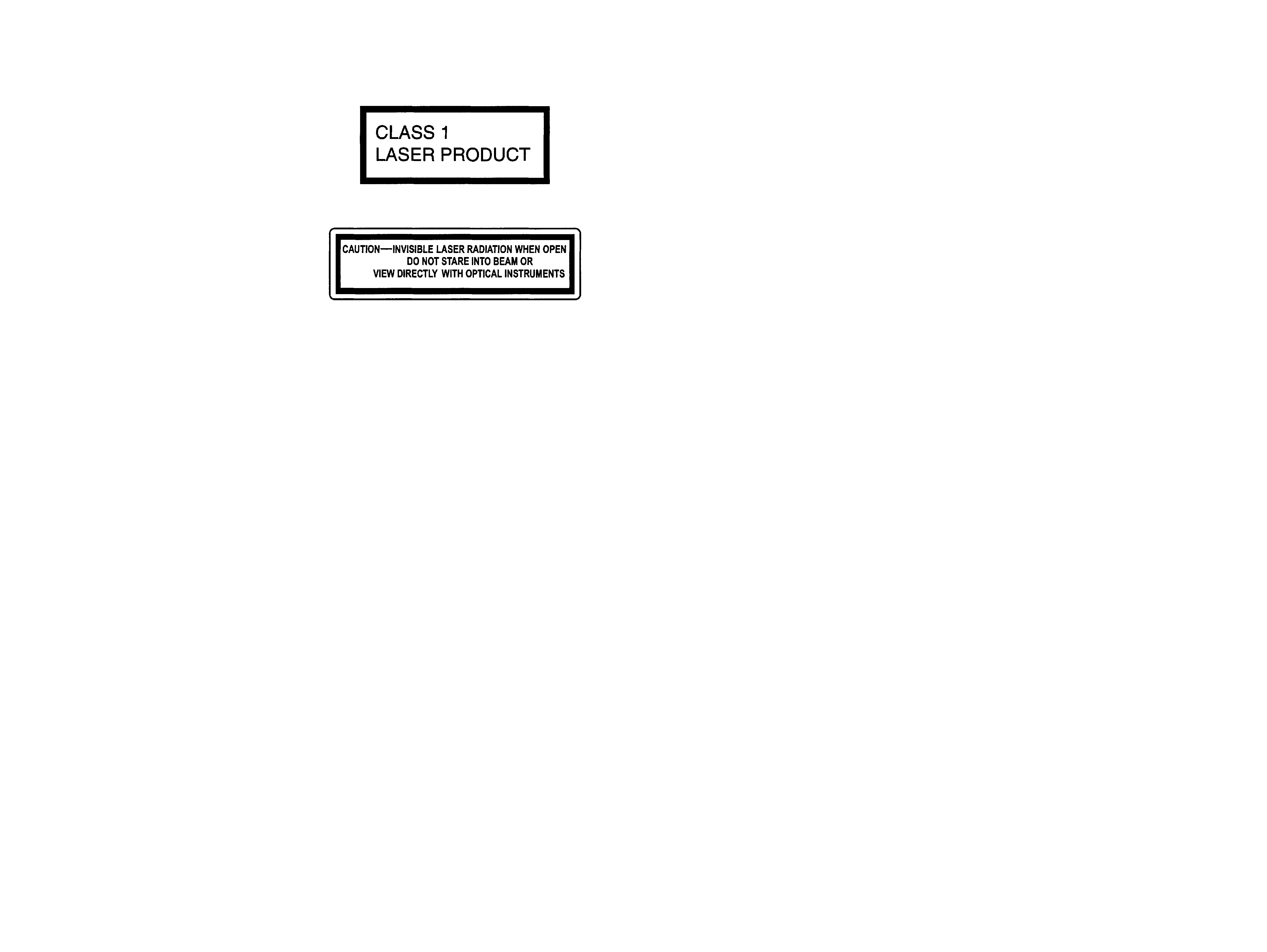
NOTES ON LASER DIODE EMISSION CHECK
The laser beam on this model is concentrated so as to be focused on
the disc reflective surface by the objective lens in the optical pick-
up block. Therefore, when checking the laser diode emission, ob-
serve from more than 30 cm away from the objective lens.
Notes on Chip Component Replacement
· Never reuse a disconnected chip component.
· Notice that the minus side of a tantalum capacitor may be dam-
aged by heat.
SERVICE NOTES
This label is located on the bottom of the chassis.
This label is located on the drive unit's internal
chassis.
When replacing the chassis (T.U) of mechanism deck which have
the "CAUTION LABEL" attached, please be sure to put a new
CAUTION LABEL (3-223-913-11) to the chassis (T.U).
CDX-L350/L360
3
CDX-L350/L360
SECTION 1
GENERAL
This section is extracted
from instruction manual.
4
CDX-L350/L360
55
CDX-L350/L360