SERVICE MANUAL
US Model
AEP Model
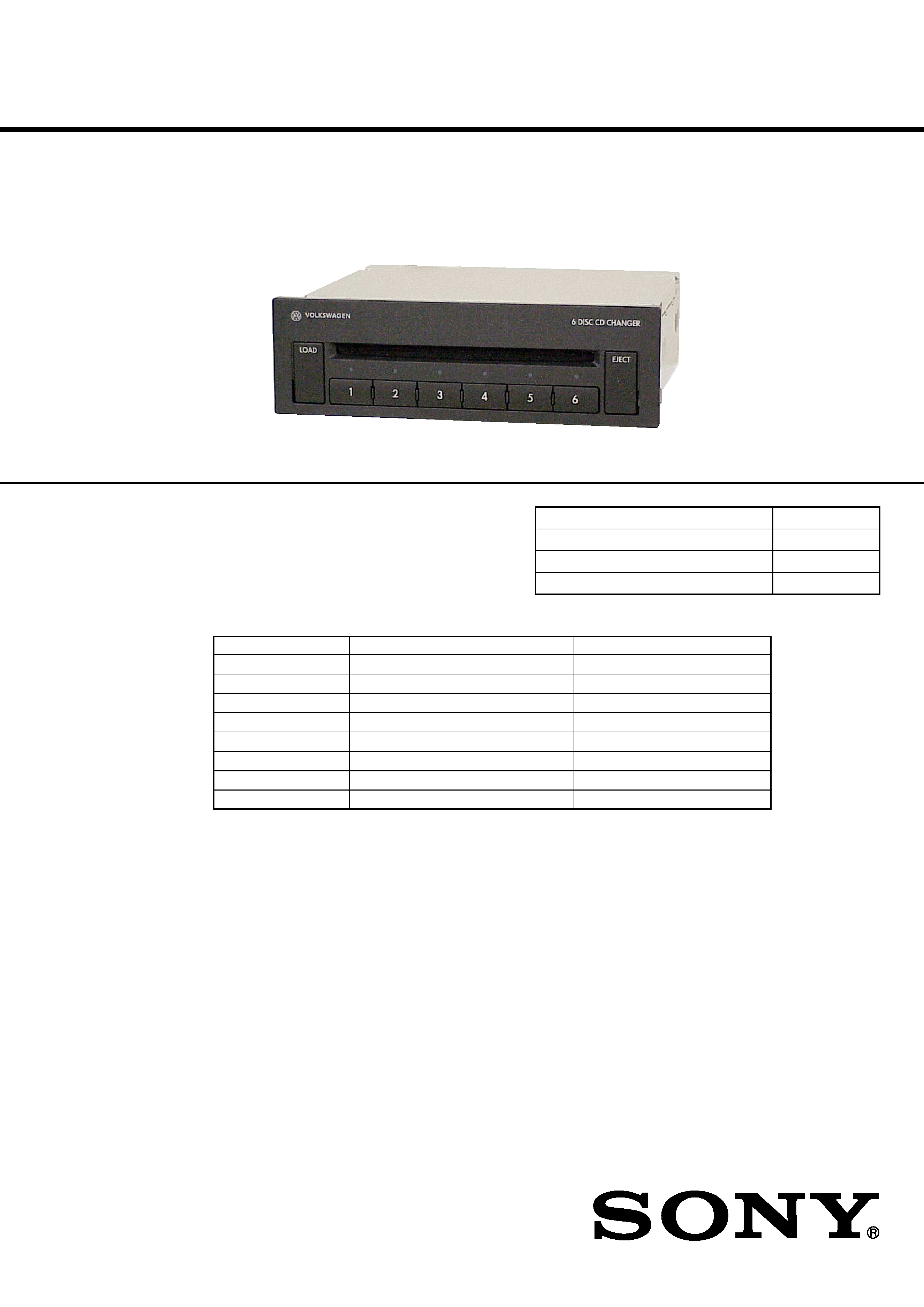
CDX-5V662
(VW No.: 1J0 035 110)
Ver 1.1 2002.09
9-874-019-02
Sony Corporation
2002I0500-1
e Vehicle Company
C
2002.09
Published by Sony Engineering Corporation
6 DISC IN-DASH CD CHANGER
Connectable head units
Manufacture
Model name
VW No.
SONY
Gamma
1J0 035 186D
Clarion
Premium
1J0 035 180D
Philips
Beta
1J0 035 152B
Blaupunkt
Gamma
1J0 035 186B
Blaupunkt
Beta
6X0 035 152
Grundig
Beta
1J0 035 152 E
Blaupunkt
Radio Navigation (Color LED)
3B0 035 191 A
Blaupunkt
Radio Navigation
1J0 035 191
Model Name Using Similar Mechanism
NEW
Main Block Assy
MG-160V-154
CD Drive Mechanism Type
MG-161V-178
Optical Pick-up Name
KSS-660C
2
CDX-5V662
TABLE OF CONTENTS
1.
SERVICING NOTES ................................................ 3
2.
DISASSEMBLY
2-1. Disassembly Flow ...........................................................
4
2-2. Cover (Up) .......................................................................
5
2-3. Front Panel Section .........................................................
5
2-4. Mechanism Deck (MG-161V-178) .................................
6
2-5. MAIN-VW Board ...........................................................
7
2-6. Slide Variable Resistor
(Elevator Height Sensor) (RV1) .....................................
8
2-7. ASSIST Board .................................................................
8
2-8. L Motor Assy (Loading) (M103) ....................................
9
2-9. Chassis (TR.V) Main Assy .............................................
9
2-10. Bracket (DE) Main Assy ................................................. 10
2-11. Slider (TOP) Assy ........................................................... 10
2-12. Bracket (UD) Assy .......................................................... 11
2-13. Guide (Chuck) ................................................................. 11
2-14. Setting The OP Block Assy In The Highest Position ..... 12
2-15. Address Detection Flexible Board .................................. 13
2-16. Torsion Spring (OP) ........................................................ 13
2-17. OP Block Assy ................................................................ 14
3.
ELECTRICAL ADJUSTMENTS ......................... 15
4.
DIAGRAMS
4-1. Block Diagram MAIN Section ................................. 38
4-2. Block Diagram
DISPLAY/POWER SUPPLY Section ..................... 39
4-3. Note for Printed Wiring Boards and
Schematic Diagrams ....................................................... 40
4-4. Schematic Diagram MAIN Section (1/3) ................. 41
4-5. Schematic Diagram MAIN Section (2/3) ................. 42
4-6. Schematic Diagram MAIN Section (3/3) ................. 43
4-7. Printed Wiring Boards
MAIN Section (Component Side) ............................ 44
4-8. Printed Wiring Board
MAIN Section (Conductor Side) .............................. 45
4-9. Printed Wiring Board KEY Board ............................ 46
4-10. Schematic Diagram KEY Board .............................. 47
4-11. Printed Wiring Board F2 Board ................................ 48
4-12. Schematic Diagram F2 Board ................................... 49
4-13. Printed Wiring Board F1 Board ................................ 50
4-14. Schematic Diagram F1 Board ................................... 50
4-15. IC Pin Function Description ........................................... 55
5.
EXPLODED VIEWS
5-1. General ............................................................................ 61
5-2. Front Panel Section ......................................................... 62
5-3. Main Block Assy (V) Section-1 (MG-160V-154) .......... 63
5-4. Main Block Assy (V) Section-2 (MG-160V-154) .......... 64
5-5. Mechanism Deck Section-1 (MG-161V-178) ................ 65
5-6. Mechanism Deck Section-2 (MG-161V-178) ................ 66
6.
ELECTRICAL PARTS LIST ............................... 67
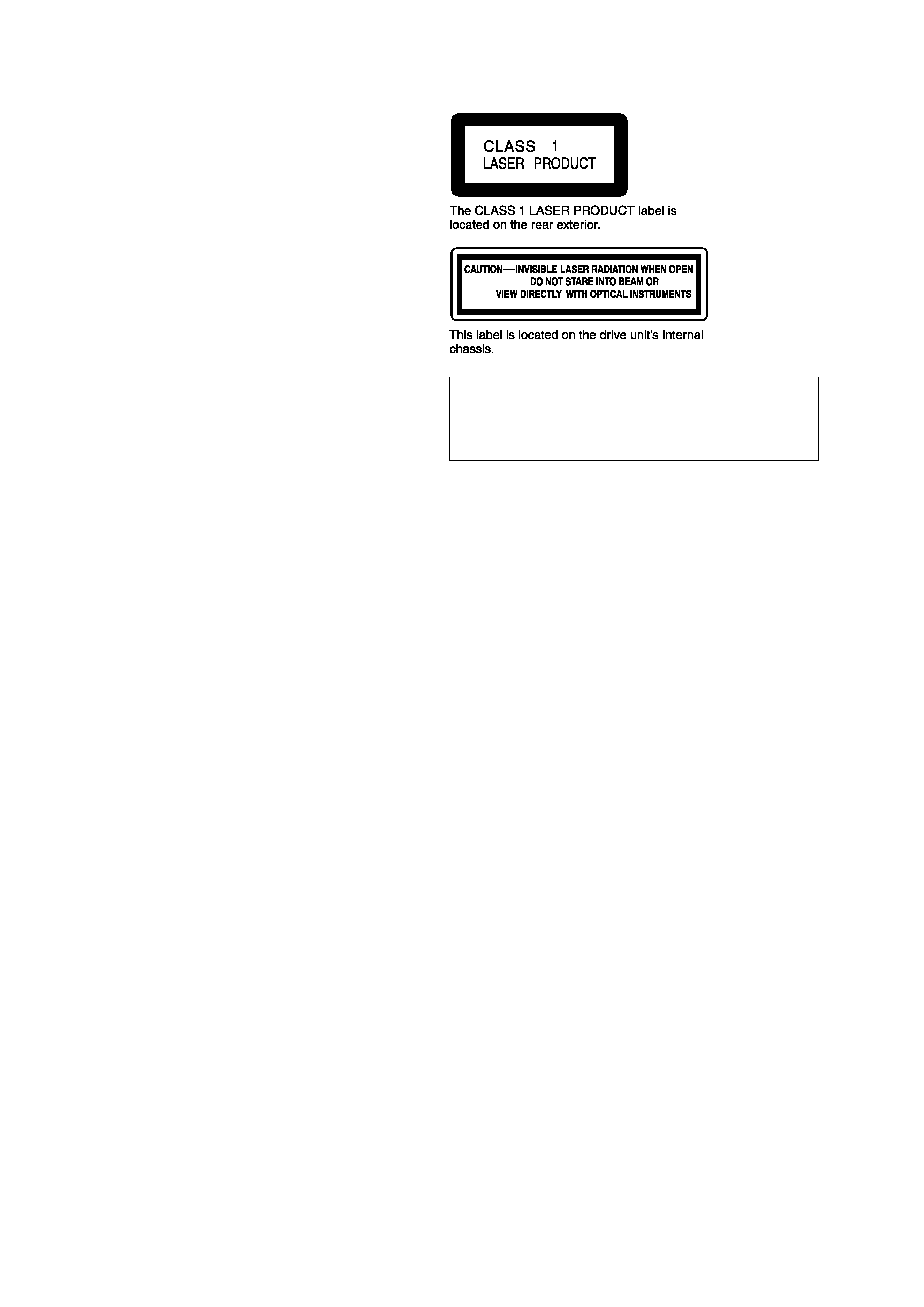
SAFETY-RELATED COMPONENT WARNING!!
COMPONENTS IDENTIFIED BY MARK 0 OR DOTTED
LINE WITH MARK 0 ON THE SCHEMATIC DIAGRAMS
AND IN THE PARTS LIST ARE CRITICAL TO SAFE
OPERATION. REPLACE THESE COMPONENTS WITH
SONY PARTS WHOSE PART NUMBERS APPEAR AS
SHOWN IN THIS MANUAL OR IN SUPPLEMENTS PUB-
LISHED BY SONY.
Notes on chip component replacement
·Never reuse a disconnected chip component.
· Notice that the minus side of a tantalum capacitor may be dam-
aged by heat.
Flexible Circuit Board Repairing
·Keep the temperature of the soldering iron around 270 °C dur-
ing repairing.
· Do not touch the soldering iron on the same conductor of the
circuit board (within 3 times).
· Be careful not to apply force on the conductor when soldering
or unsoldering.
CAUTION
Use of controls or adjustments or performance of procedures
other than those specified herein may result in hazardous ra-
diation exposure.

3
CDX-5V662
SECTION 1
SERVICING NOTES
The laser diode in the optical pick-up block may suffer electro-
static break-down because of the potential difference generated
by the charged electrostatic load, etc. on clothing and the human
body.
During repair, pay attention to electrostatic break-down and also
use the procedure in the printed matter which is included in the
repair parts.
The flexible board is easily damaged and should be handled with
care.
Laser Diode Properties
· Material: GaAlAs
·Wavelength: 780 nm
· Emission Duration: continuous
· Laser Output Power: less than 44.6
µW*
*This output is the value measured at a distance of 200 mm
from the objective lens surface on the Optical Pick-up Block.
NOTES ON LASER DIODE EMISSION CHECK
The laser beam on this model is concentrated so as to be focused
on the disc reflective surface by the objective lens in the optical
pick-up block. Therefore, when checking the laser diode emis-
sion, observe from more than 30 cm away from the objective lens.
· HOW TO EJECT THE DISC MANUALLY
When an electric current can be applied, eject the disc forcibly by
moving each motor manually.
(See "3. Electrical Adjustment 3. Mechanism check mode" on
page 26).
NOTES ON HANDLING THE OPTICAL PICK-UP
BLOCK OR BASE UNIT
CDX-5V662
4
SECTION 2
DISASSEMBLY
· This set can be disassembled in the order shown below.
2-1.
DISASSEMBLY FLOW
2-3. FRONT PANEL SECTION
(Page 5)
2-2. COVER (UP)
(Page 5)
2-4. MECHANISM DECK (MG-161V-178)
(Page 6)
2-5. MAIN-VW BOARD
(Page 7)
2-7. ASSIST BOARD
(Page 8)
2-8. L MOTOR ASSY
(LOADING) (M103)
(Page 9)
2-9. CHASSIS (TR.V) MAIN ASSY
(Page 9)
2-10. BRACKET (DE) MAIN ASSY
(Page 10)
2-11. SLIDER (TOP) ASSY
(Page 10)
2-12. BRACKET (UD) ASSY
(Page 11)
2-13. GUIDE (CHUCK)
(Page 11)
2-14. SETTING THE OP BLOCK ASSY IN THE HIGHEST POSITION
(Page 12)
2-15. ADDRESS DETECTION FLEXIBLE BOARD
(Page 13)
2-16. TORSION SPRING (OP)
(Page 13)
2-17. OP BLOCK ASSY
(Page 14)
2-6. SLIDE VARIABLE RESISTOR
(ELEVATOR HEIGHT SENSOR) (RV1)
(Page 8)
SET
CDX-5V662
5
Note: Follow the disassembly procedure in the numerical order given.
Note: Screws and washers cannot be re-used.
Please replace to brand-new ones once screws and washers are removed.
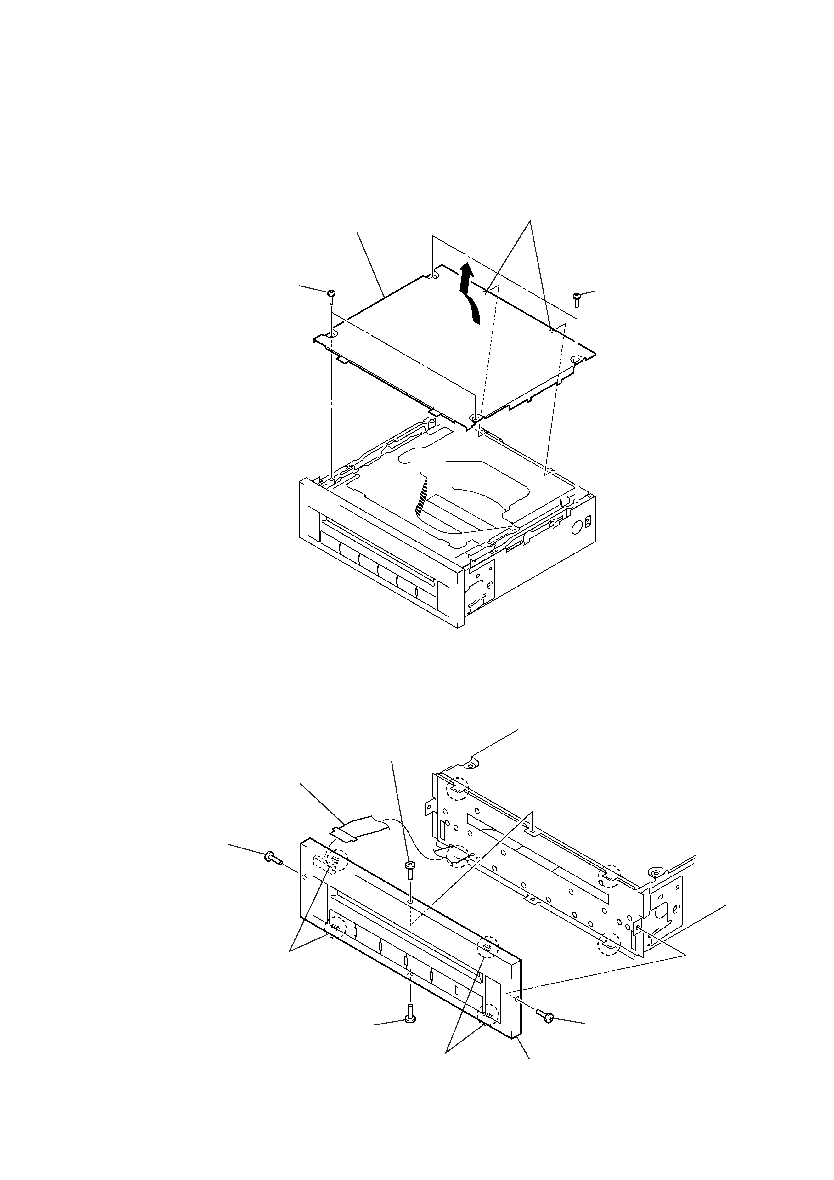
2-2.
COVER (UP)
2-3.
FRONT PANEL SECTION
1
two screws
(PTT2.6
× 6)
1
two screws
(PTT2.6
× 6)
3
Remove the cover (up)
in the direction of the arrow.
2
two bosses
1
screw
(2
× 4.5)
1
screw
(2
× 4.5)
1
screw
(2
× 4.5)
1
screw
(2
× 4.5)
4
front panel section
2
two claws
2
two claws
3
key flexible board
(CN1)