HCD-J300
AEP Model
UK Model
E Model
SERVICE MANUAL
MICRO HI-FI COMPONENT SYSTEM
-- Continued on next page --
SPECIFICATIONS
HCD-J300 is the Amplifier, MD deck, CD
player, Tape player and Tuner section in
CMT-DC500MD.
Model Name Using Similar Mechanism
HCD-CP500K/CP500MD
CD Mechanism Type
CDM55F-K4BD43
Base Unit Type
BU-K4BD43
Optical Pick-up Type
KSM-213DHAP
Model Name Using Similar Mechanism
HCD-CP500K/CP500MD
MD Mechanism Type
MDM-7B
Optical Pick-up Type
KMS-260B
Model Name Using Similar Mechanism
HCD-CP500K/CP500MD
Tape Transport Mechanism Type
Mech deck
CD
Section
MD
Section
Tape deck
Section
Sony Corporation
Home Audio Company
Published by Sony Engineering Corporation
9-873-173-02
2001J1600-1
© 2001.10
Ver 1.1 2001. 10
Amplifier section
European model:
DIN power output (rated): 30 + 30 W
(6 ohms at 1 kHz, DIN)
Continuous RMS power output (reference):
35 + 35 W
(6 ohms at 1 kHz, 10%
THD)
Music power output (reference):
85 + 85 W
Other models:
The following measured at 230 V AC, 60 Hz
DIN power output (rated): 30 + 30 W
(6 ohms at 1 kHz, DIN)
Continuous RMS power output (reference):
35 + 35 W
(6 ohms at 1 kHz, 10%
THD)
The following measured at 220 V AC, 60 Hz
DIN power output (rated): 24 + 24 W
(6 ohms at 1 kHz, DIN)
Continuous RMS power output (reference):
27 + 27 W
(6 ohms at 1 kHz, 10%
THD)
Inputs
ANALOG IN (phono jacks):
Sensitivity 250 mV,
impedance 47 kilohms
DIGITAL OPTICAL IN (Supported sampling
frequencies: 32 kHz, 44.1 kHz and 48 kHz)
Outputs
PHONES (stereo minijack):
Accepts headphones with
an impedance of 8 ohms
or more
SPEAKER:
Accepts impedance of 6 to
16 ohms

2
HCD-J300
CD player section
System
Compact disc and digital
audio system
Laser
Semiconductor laser
(
= 780 nm)
Emission
duration: continuous
Wavelength
780 790 nm
Frequency response
2 Hz 20 kHz (
±0.5 dB)
Tape player section
Recording system
4-track 2-channel stereo
Frequency response
50 13,000 Hz (
±3 dB),
using a Sony TYPE I
cassette
Wow and flutter
±0.15% W. Peak (IEC)
0.1% W. RMS (NAB)
±0.2% W. Peak (DIN)
MD deck section
System
MiniDisc digital audio
system
Laser
Semiconductor laser
(
=780 nm)
Emission duration:
continuous
Sampling frequency
44.1 kHz
Frequency response
5 Hz 20 kHz
Tuner section
FM stereo, FM/AM superheterodyne tuner
FM tuner section
Tuning range
87.5 108.0 MHz
(50-kHz step)
Antenna
FM wire antenna
Antenna terminals
75 ohm unbalanced
Intermediate frequency
10.7 MHz
AM tuner section
Tuning range
European model:
531 1,602 kHz
(with the tuning interval
set at 9 kHz)
Other models:
530 1,710 kHz
(with the tuning interval
set at 10 kHz)
531 1,602 kHz
(with the tuning interval
set at 9 kHz)
Antenna
AM loop antenna, external
antenna terminal
Intermediate frequency
450 kHz
General
Power requirements
European model:
230 V AC, 50/60 Hz
Hong Kong model:
220 240 V AC,
50/60 Hz
Other models:
110 120 V or 220
240 V AC , 50/60 Hz
Adjustable with voltage
selector
Power consumption
European model:
See the nameplate
0.5 W (in the standby
mode)
Other models:
See the nameplate
Dimensions (w/h/d)
Approx. 190
× 253 ×
345 mm incl. projecting
parts and controls
Mass
Approx. 7.0 kg
Design and specifications are subject to change
without notice.
3
HCD-J300
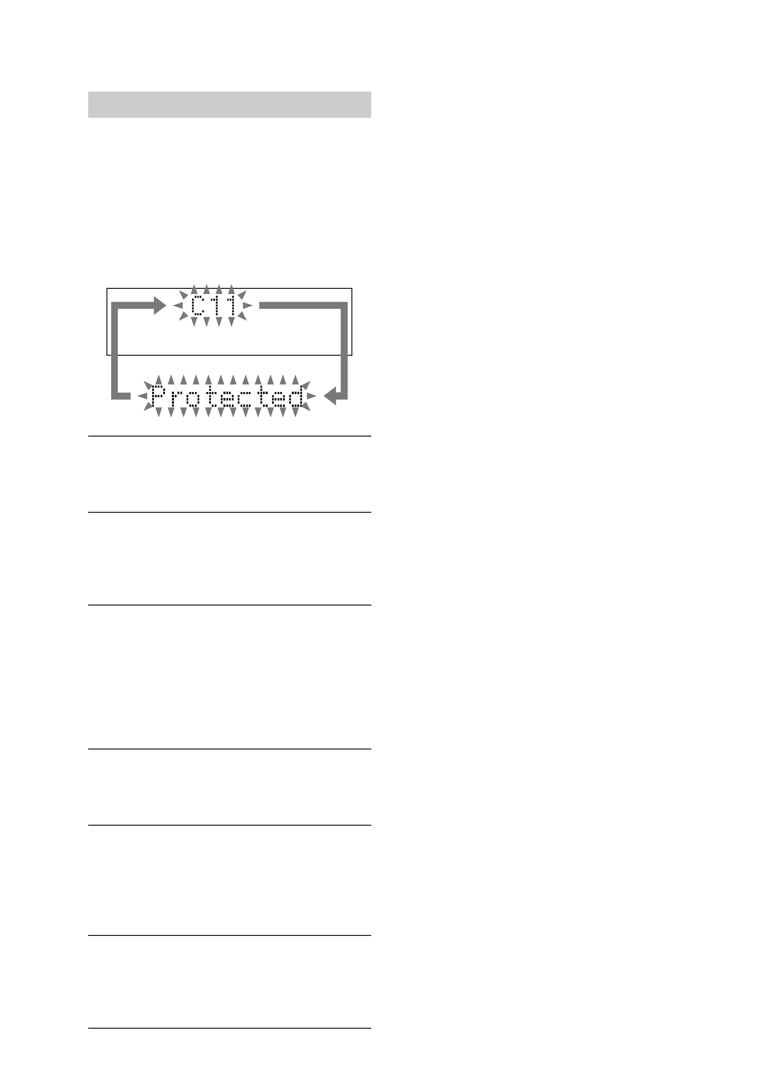
Self-diagnosis display
This system has a Self-diagnosis display
function to let you know if there is a system
malfunction. The display shows a code made
up of three letters and a message alternately to
show you the problem. To solve the problem
refer to the following list. If any problem
persists, consult your nearest Sony dealer.
C11/Protected
The MD is protected against erasure.
Remove the MD and slide the tab to close the
slot (see page 16).
C12/Cannot Copy
You tried to record a CD or MD with a format that
the system does not support, such as a CD-ROM.
p Remove the disc and turn off the system once,
then turn it on again.
C13/REC Error
Recording could not be performed properly.
p Move the system to a stable place, and start
recording over from the beginning.
The MD is dirty or scratched, or the MD does not
meet the standards.
p Replace the MD and start recording over from
the beginning.
C13/Read Error
The MD deck cannot read the disc information
properly.
p Remove the MD once, then load it again.
C14/Toc Error
The MD deck cannot read the disc information
properly.
p Replace the MD.
p Erase all the recorded contents of the MD using
All Erase Function (see page 27).
C41/Cannot Copy
The sound source is a copy of commercially
available music software.
p The Serial Copy Management System prevents
making a digital copy (see page 47).
1. SERVICING NOTES ······················································ 4
2. GENERAL ·········································································· 9
3. DISASSEMBLY ······························································ 11
4. TEST MODE ··································································· 21
5. MECHANICAL ADJUSTMENTS ···························· 27
6. ELECTRICAL ADJUSTMENTS ······························ 27
7. DIAGRAMS
7-1. CIRCUIT BOARDS LOCATION ····································· 40
7-2. BLOCK DIAGRAM CD SECTION ··························· 42
BLOCK DIAGRAM MAIN SECTION ······················ 43
BLOCK DIAGRAM MD SECTION ·························· 44
BLOCK DIAGRAM PANEL SECTION ···················· 45
7-3. PRINTED WIRING BOARD CD BOARD ················ 46
7-4. SCHEMATIC DIAGRAM CD BOARD ····················· 47
7-5. PRINTED WIRING BOARD BD BOARD ················ 48
7-6. SCHEMATIC DIAGRAM BD BOARD (1/2) ············ 49
7-7. SCHEMATIC DIAGRAM BD BOARD (2/2) ············ 50
7-8. PRINTED WIRING BOARDS AUDIO SECTION ···· 51
7-9. SCHEMATIC DIAGRAM AUDIO SECTION (1/2) ··· 52
7-10. SCHEMATIC DIAGRAM AUDIO SECTION (2/2) ··· 53
7-11. PRINTED WIRING BOARD TC BOARD ················· 54
7-12. SCHEMATIC DIAGRAM TC BOARD ······················ 55
7-13. PRINTED WIRING BOARD DIGITAL BOARD ······ 56
7-14 SCHEMATIC DIAGRAM DIGITAL BOARD ··········· 57
7-15. PRINTED WIRING BOARDS CONTROL SECTION ··· 58
7-16 SCHEMATIC DIAGRAM CONTROL BOARD ········ 59
7-17. PRINTED WIRING BOARD POWER BOARD ········ 60
7-18. SCHEMATIC DIAGRAM POWER BOARD ············· 60
7-19. IC BLOCK DIAGRAMS ·················································· 61
7-20. IC Pin Function Description ·············································· 63
8. EXPLODED VIEWS ····················································· 71
9. ELECTRICAL PARTS LIST ····································· 80
TABLE OF CONTENTS
4
HCD-J300
SECTION 1
SERVICING NOTE
This appliance is classified as a CLASS 1 LASER product. The
CLASS 1 LASER PRODUCT MARKING is located on the rear
exterior.
Laser component in this product is capable
of emitting radiation exceeding the limit for
Class 1.
CAUTION
Use of controls or adjustments or performance of procedures
other than those specified herein may result in hazardous radiation
exposure.
Notes on chip component replacement
· Never reuse a disconnected chip component.
· Notice that the minus side of a tantalum capacitor may be
damaged by heat.
Flexible Circuit Board Repairing
· Keep the temperature of soldering iron around 270°C
during repairing.
· Do not touch the soldering iron on the same conductor of the
circuit board (within 3 times).
· Be careful not to apply force on the conductor when soldering
or unsoldering.
NOTES ON HANDLING THE OPTICAL PICK-UP
BLOCK OR BASE UNIT
The laser diode in the optical pick-up block may suffer electrostatic
break-down because of the potential difference generated by the
charged electrostatic load, etc. on clothing and the human body.
During repair, pay attention to electrostatic break-down and also
use the procedure in the printed matter which is included in the
repair parts.
The flexible board is easily damaged and should be handled with
care.
FOR CD
NOTES ON LASER DIODE EMISSION CHECK
The laser beam on this model is concentrated so as to be focused on
the disc reflective surface by the objective lens in the optical pick-
up block. Therefore, when checking the laser diode emission,
observe from more than 30 cm away from the objective lens.
FOR MD
NOTES ON LASER DIODE EMISSION CHECK
Never look into the laser diode emission from right above when
checking it for adjustment. It is feared that you will lose your sight.
This caution
label is
located inside
the unit.
SAFETY-RELATED COMPONENT WARNING!!
COMPONENTS IDENTIFIED BY MARK 0 OR DOTTED LINE WITH
MARK 0 ON THE SCHEMATIC DIAGRAMS AND IN THE PARTS
LIST ARE CRITICAL TO SAFE OPERATION. REPLACE THESE
COMPONENTS WITH SONY PARTS WHOSE PART NUMBERS
APPEAR AS SHOWN IN THIS MANUAL OR IN SUPPLEMENTS
PUBLISHED BY SONY.
5
HCD-J300
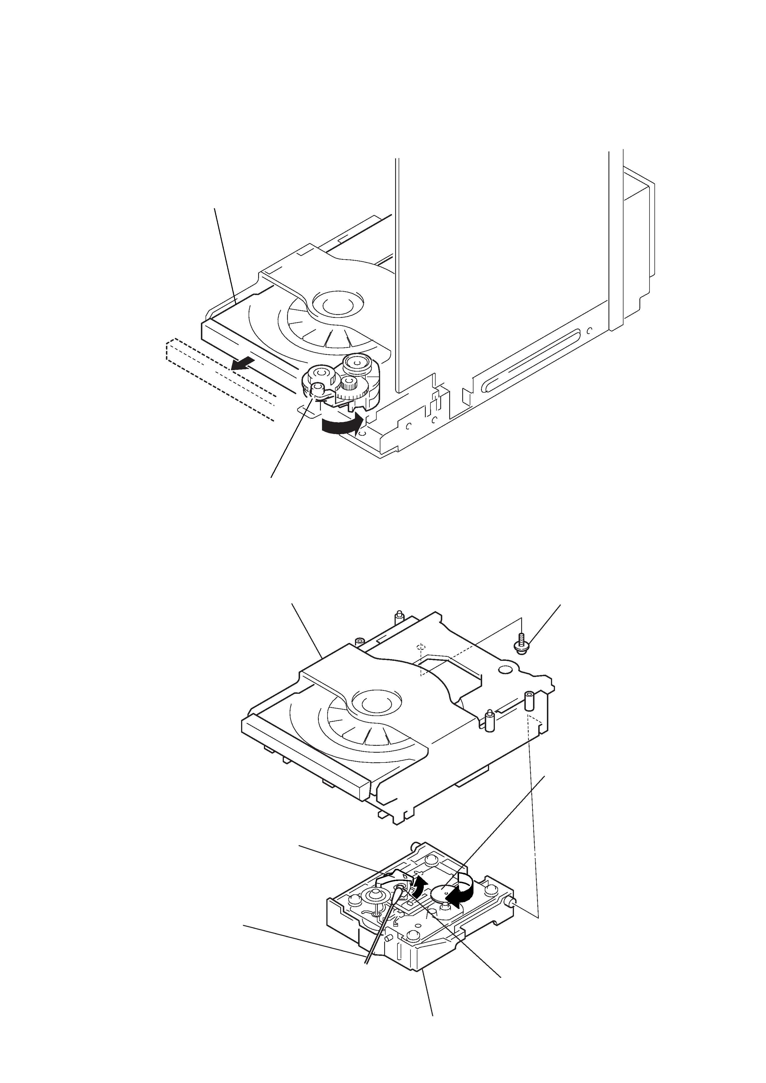
DRAWING OUT THE TRAY DURING POWER OUT
CLEANING THE OPTICAL PICK-UP (CD PLAYER)
Tray
Move the cam block in the direction of the arrow by fingers.
1
Floating screw
3
BU-K4BD43
2
CD mechanism deck
4
Rotate it in the
direction of the arrow A.
A
B
5
Move it in the
direction of the arrow B.
6
Clean the lens block
by cotton swab
Optical pick-up