1
Ver 1.0 2004. 01
Model Name Using Similar Mechanism
CDX-R3000/R3000T
CD Drive Mechanism Type
MG-611XC-186//Q
Optical Pick-up Name
KSS1000E
SERVICE MANUAL
US Model
Canadian Model
CDC-X104/X144
AEP Model
UK Model
CDC-R104/X104
CDC-R104/X104/X144
AUDIO POWER SPECIFICATIONS (US MODEL)
POWER OUTPUT AND TOTAL HARMONIC DISTORTION
22 watts per channel minimum continuous average power into
4 ohms, 4 channels driven from 20 Hz to 20 kHz with no more
than 5% total harmonic distortion.
Tuner section
FM
Tuning range
US, Canadian Model:
87.5 107.9 MHz
AEP, UK Model:
87.5 108 MHz
Antenna terminal
External antenna connector
Intermediate frequency 10.7 MHz/450 kHz
Usable sensitivity
9 dBf
Selectivity
75 dB at 400 kHz
Signal-to-noise ratio
67 dB (stereo),
69 dB (mono)
Harmonic distortion at 1 kHz
0.5% (stereo),
0.3% (mono)
Separation
35 dB at 1 kHz
Frequency response
30 15,000 Hz
AM (US, Canadian Model)
Tuning range
530 1,710 kHz
Antenna terminal
External antenna connector
Intermediate frequency 10.7 MHz/450 kHz
Sensitivity
30 µV
MW/LW (AEP, UK Model)
Tuning range
MW: 531 1,602 kHz
LW: 153 279 kHz
Antenna terminal
External antenna connector
Intermediate frequency 10.7 MHz/450 kHz
Sensitivity
MW: 30 µV
LW: 40 µV
CD player section
Signal-to-noise ratio
US, Canadian Model: 110 dB
AEP, UK Model: 120 dB
Frequency response
10 20,000 Hz
Wow and flutter
Below measurable limit
SPECIFICATIONS
Power amplifier section
Outputs
Speaker outputs
(sure seal connectors)
Speaker impedance
4 8 ohms
Maximum power output 45 W
× 4 (at 4 ohms)
General
Outputs
Audio outputs terminal (rear/sub switchable)
Power antenna relay control terminal
Power amplifier control terminal
Inputs
Telephone ATT control terminal (AEP, UK Model)
Antenna input terminal
Tone controls
Low: ±10 dB at 60 Hz (HIP-HOP)
Mid: ±10 dB at 1 kHz (HIP-HOP)
High: ±10 dB at 10 kHz (HIP-HOP)
Power requirements
12 V DC car battery (negative ground)
Dimensions
Approx. 178
× 50 × 176 mm
(7 1/8
× 2 × 7 in.) (w/h/d)
Mounting dimensions
Approx. 182
× 53 × 161 mm
(7 1/4
× 2 1/8 × 6 3/8 in.) (w/h/d)
Mass
Approx. 1.2 kg (2 lb. 10 oz.)
Supplied accessories
Parts for installation and connections (1 set)
Front panel case (1)
Design and specifications are subject to change without
notice.
· The tuner and CD sections have no adjustments.
Sony Corporation
e Vehicle Company
Published by Sony Engineering Corporation
9-877-520-01
2004A04-1
© 2004. 01
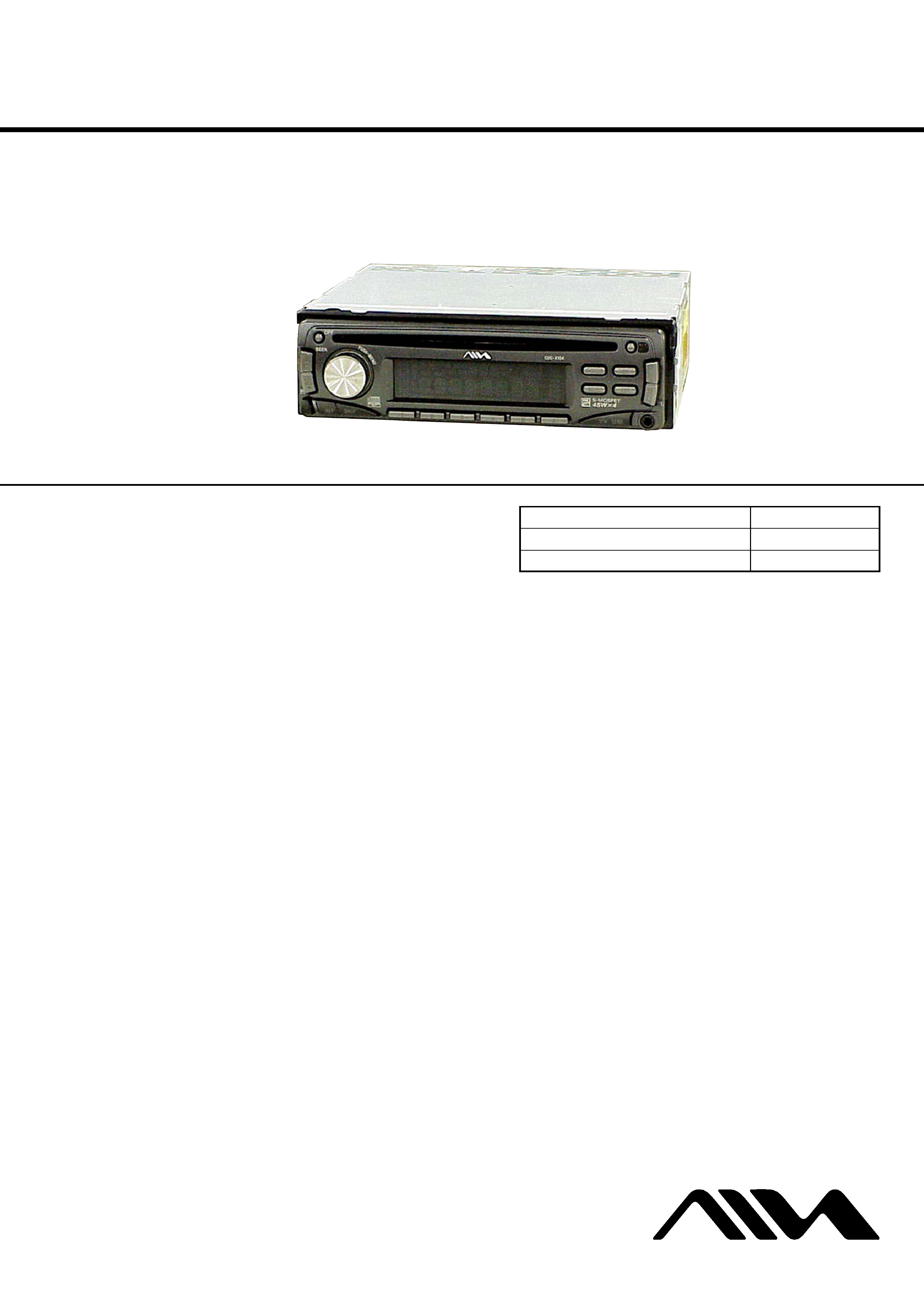
Photo: CDC-X104
FM/AM COMPACT DISC PLAYER
US, Canadian model
FM/MW/LW COMPACT DISC PLAYER
AEP, UK model
2
CDC-R104/X104/X144
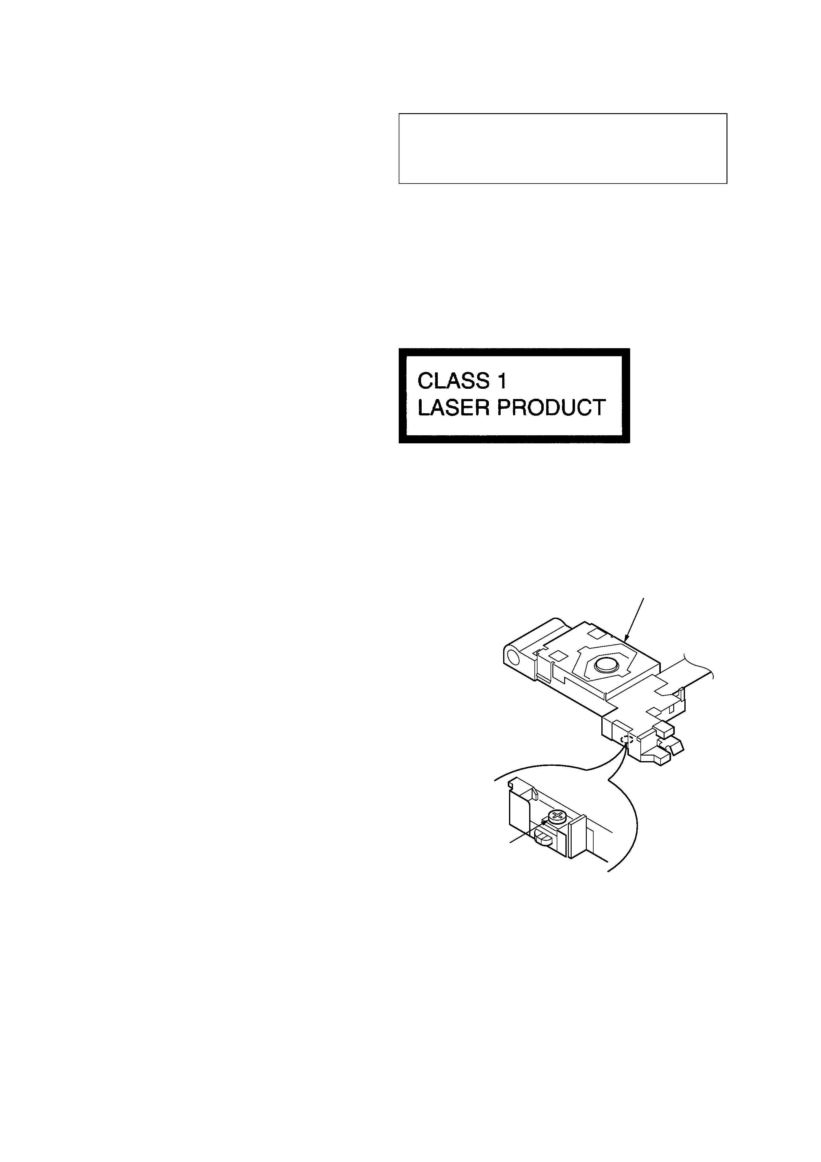
If the optical pick-up block is defective, please replace the whole
optical pick-up block.
Never turn the semi-fixed resistor located at the side of optical
pick-up block.
CAUTION
Use of controls or adjustments or performance of procedures
other than those specified herein may result in hazardous
radiation exposure.
SAFETY-RELATED COMPONENT WARNING!!
COMPONENTS IDENTIFIED BY MARK 0 OR DOTTED LINE
WITH MARK 0 ON THE SCHEMATIC DIAGRAMS AND IN
THE PARTS LIST ARE CRITICAL TO SAFE OPERATION.
REPLACE THESE COMPONENTS WITH SONY PARTS WHOSE
PART NUMBERS APPEAR AS SHOWN IN THIS MANUAL OR
IN SUPPLEMENTS PUBLISHED BY SONY.
ATTENTION AU COMPOSANT AYANT RAPPORT
À LA SÉCURITÉ!!
LES COMPOSANTS IDENTIFIÉS PAR UNE MARQUE 0 SUR LES
DIAGRAMMES SCHÉMATIQUES ET LA LISTE DES PIÈCES
SONT CRITIQUES POUR LA SÉCURITÉ DE FONCTIONNEMENT.
NE REMPLACER CES COMPOSANTS QUE PAR DES PIÈCES
SONY DONT LES NUMÉROS SONT DONNÉS DANS CE MANUEL
OU DANS LES SUPPLÉMENTS PUBLIÉS PAR SONY.
NOTES ON HANDLING THE OPTICAL PICK-UP BLOCK
OR BASE UNIT
The laser diode in the optical pick-up block may suffer electrostatic
breakdown because of the potential difference generated by the
charged electrostatic load, etc. on clothing and the human body.
During repair, pay attention to electrostatic breakdown and also use
the procedure in the printed matter which is included in the repair
parts.
The flexible board is easily damaged and should be handled with
care.
NOTES ON LASER DIODE EMISSION CHECK
The laser beam on this model is concentrated so as to be focused on
the disc reflective surface by the objective lens in the optical pick-
up block. Therefore, when checking the laser diode emission, ob-
serve from more than 30 cm away from the objective lens.
Notes on Chip Component Replacement
· Never reuse a disconnected chip component.
· Notice that the minus side of a tantalum capacitor may be dam-
aged by heat.
TEST DISCS
This set can playback CD-R and CD-ROM discs. The following
test discs should be used to check the capability:
CD-R test disc TCD-R082LMT (Part No. J-2502-063-1)
CD-RW test disc TCD-W082L (Part No. J-2502-063-2)
SERVICE NOTES
optical pick-up
semi-fixed resistor
· US, Canadian model
· AEP, UK model
CAUTION
Use of controls or adjustments or performance of procedures other
than those specified herein may result in hazardous radiation
exposure.
This compact disc player is classified as a CLASS 1 LASER
product. The CLASS 1 LASER PRODUCT label is located on the
exterior.
This label is located on the bottom of the chassis.
3
CDC-R104/X104/X144
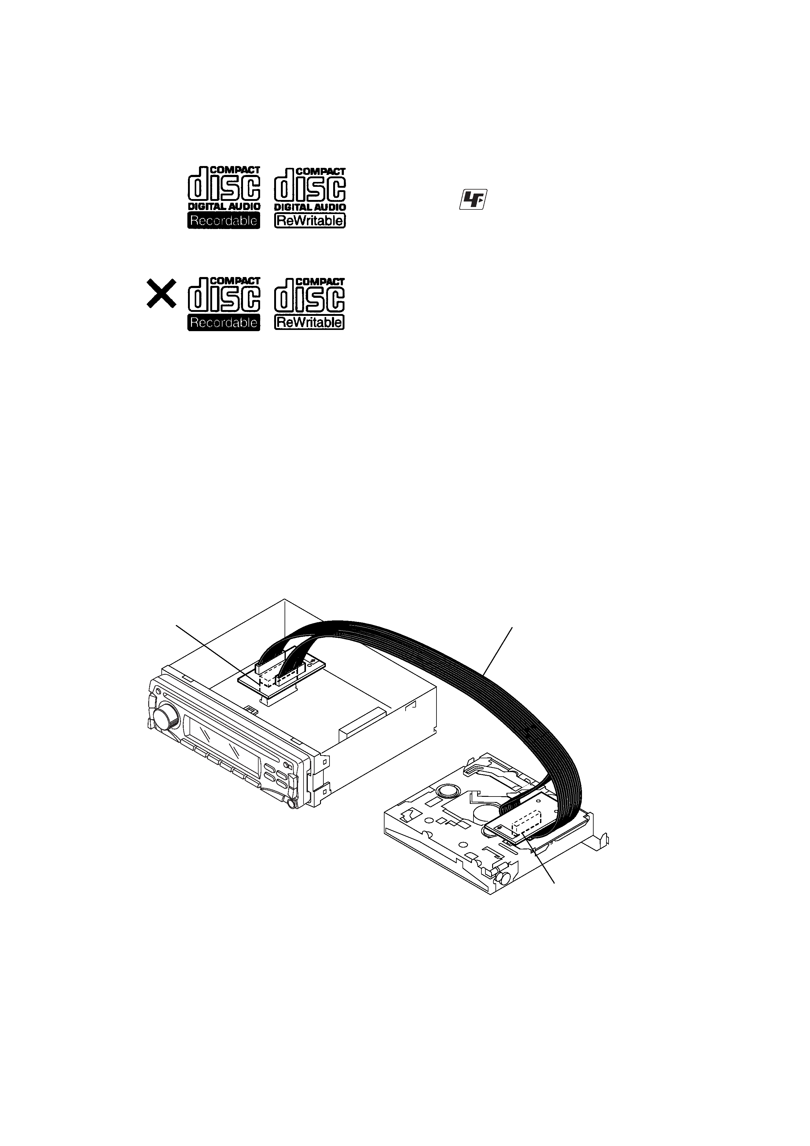
Notes on CD-R/CD-RW discs
· You can play CD-Rs (recordable CDs)/CD-RWs (rewritable CDs)
designed for audio use on this unit.
Look for these marks to distinguish CD-Rs/CD-RWs for audio
use.
These marks denote that a disc is not for audio use.
· Some CD-Rs/CD-RWs (depending on the equipment used for
its recording or the condition of the disc) may not play on this
unit.
· You cannot play a CD-R/CD-RW that is not finalized.
A process necessary for a recorded CD-R/CD-RW disc to be
played on the audio CD player.
EXTENSION CABLE AND SERVICE POSITION
When repairing or servicing this set, connect the jig (extension cable)
as shown below.
· Connect the MAIN board (CN301) and the SERVO board (CN1)
with the extension cable (Part No. J-2502-076-1).
z
UNLEADED SOLDER
Boards requiring use of unleaded solder are printed with the lead
free mark (LF) indicating the solder contains no lead.
(Caution: Some printed circuit boards may not come printed with
the lead free mark due to their particular size.)
: LEAD FREE MARK
Unleaded solder has the following characteristics.
· Unleaded solder melts at a temperature about 40°C higher than
ordinary solder.
Ordinary soldering irons can be used but the iron tip has to be
applied to the solder joint for a slightly longer time.
Soldering irons using a temperature regulator should be set to
about 350°C.
Caution: The printed pattern (copper foil) may peel away if the
heated tip is applied for too long, so be careful!
· Strong viscosity
Unleaded solder is more viscous (sticky, less prone to flow)
than ordinary solder so use caution not to let solder bridges
occur such as on IC pins, etc.
· Usable with ordinary solder
It is best to use only unleaded solder but unleaded solder may
also be added to ordinary solder.
SERVO BOARD
CN1
J-2502-076-1
MAIN BOARD
CN301

4
CDC-R104/X104/X144
TABLE OF CONTENTS
1. GENERAL
Location of Controls ................................................................ 5
Connections (US, Canadian Model) ........................................ 6
Connections (AEP, UK Model) ............................................... 7
2. DISASSEMBLY
2-1. Sub Panel Assy .................................................................... 9
2-2. CD Mechanism Block ......................................................... 9
2-3. Main Board ....................................................................... 10
2-4. Chassis (T) Sub Assy ........................................................ 10
2-5. Roller Arm Assy ................................................................ 11
2-6. Chassis (OP) Assy ............................................................. 11
2-7. Optical Pick-up ................................................................. 12
2-8. SL Motor Assy (M902) ..................................................... 12
2-9. LE Motor Assy (M903) ..................................................... 13
2-10. Servo Board ....................................................................... 13
3. DIAGRAMS
3-1. IC Pin Descriptions ........................................................... 14
3-2. Block Diagram CD Section ........................................... 18
3-3. Block Diagram Main Section ........................................ 19
3-4. Block Diagram Display Section .................................... 20
3-5. Circuit Boards Location .................................................... 20
3-6. Note for Printed Wiring Boards and
Schematic Diagrams .......................................................... 21
3-7. Waveforms ......................................................................... 21
3-8. Printed Wiring Boards CD Mechanism Section ............ 22
3-9. Schematic Diagram CD Mechanism Section ................ 23
3-10. Schematic Diagram Main Section (1/2) ........................ 24
3-11. Schematic Diagram Main Section (2/2) ........................ 25
3-12. Printed Wiring Board Main Section .............................. 26
3-13. Printed Wiring Boards Display Section ........................ 27
3-14. Schematic Diagram Display Section ............................. 28
3-15. IC Block Diagrams ............................................................ 29
4. EXPLODED VIEWS
4-1. Main Section ..................................................................... 32
4-2. Front Panel Section ........................................................... 33
4-3. CD Mechanism Section (1) ............................................... 34
4-4. CD Mechanism Section (2) ............................................... 35
4-5. CD Mechanism Section (3) ............................................... 36
4-6. CD Mechanism Section (4) ............................................... 37
5. ELECTRICAL PARTS LIST ........................................ 38
5
CDC-R104/X104/X144
SECTION 1
GENERAL
This section is extracted
from instruction manual.
LOCATION OF CONTROLS