SERVICE MANUAL
Digital Camera
VPC-S4
VPC-S4U
(Product Code : 126 678 00)
(Europe)
(PAL General)
(Product Code : 126 678 01)
(U.S.A.)
(Canada)
(Korea)
(Taiwan)
Contents
1. OUTLINE OF CIRCUIT DESCRIPTION .................... 2
2. DISASSEMBLY ........................................................ 10
3. ELECTRICAL ADJUSTMENT .................................. 12
4. USB STORAGE INFORMATION
REGISTRATION ...................................................... 17
5. TROUBLESHOOTING GUIDE ................................. 18
6. PARTS LIST ............................................................. 19
ACCESSORIES ....................................................... 19
PACKING MATERIALS ............................................ 19
CABINET & CHASSIS PARTS 1 ............................. 20
CABINET & CHASSIS PARTS 2 ............................. 21
ELECTRICAL PARTS .............................................. 22
CIRCUIT DIAGRAMS &
PRINTED WIRING BOARDS ...................................... C1
The components designated by a symbol ( ! ) in this schematic diagram designates components whose value are of
special significance to product safety. Should any component designated by a symbol need to be replaced, use only the part
designated in the Parts List. Do not deviate from the resistance, wattage, and voltage ratings shown.
CAUTION : Danger of explosion if battery is incorrectly replaced.
Replace only with the same or equivalent type recommended by the manufacturer.
Discard used batteries according to the manufacturer's instructions.
NOTE : 1. Parts order must contain model number, part number, and description.
2. Substitute parts may be supplied as the service parts.
3. N. S. P. : Not available as service parts.
Design and specification are subject to change without notice.
SX716/EX, U
REFERENCE No. SM5310586
FILE NO.
PRODUCT SAFETY NOTICE
2
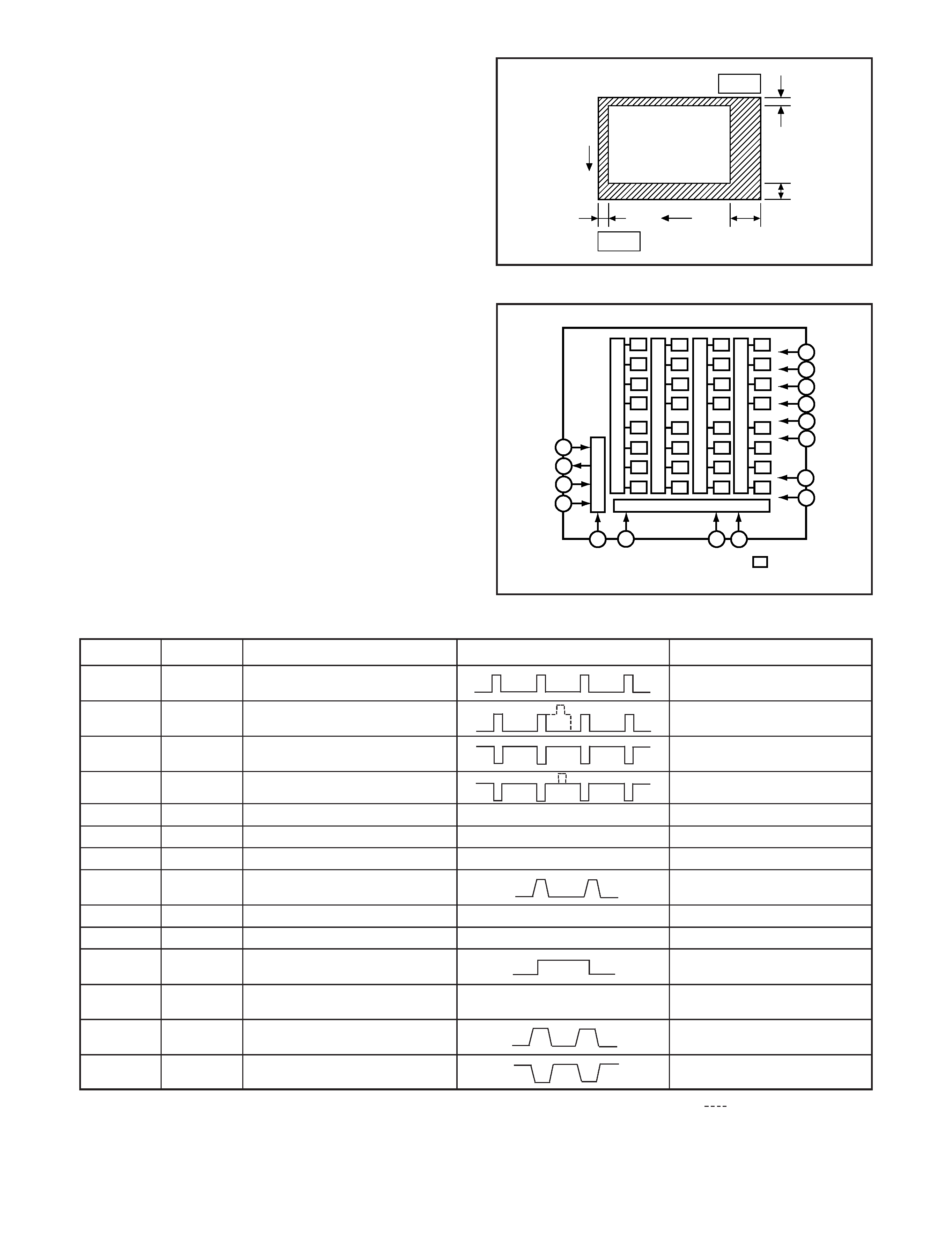
Fig. 1-1.Optical Black Location (Top View)
Pin No.
Symbol
Pin Description
Waveform
Voltage
Table 1-1. CCD Pin Description
When sensor read-out
Fig. 1-2. CCD Block Diagram
1. OUTLINE OF CIRCUIT DESCRIPTION
1-1. CP1 CIRCUIT DESCRIPTION
1. IC Configuration
IC903 (MN39483PJJ)
CCD imager
IC901 (AN20101A)
V driver
IC906 (AD9948KCPZ)
CDS, AGC, A/D converter
2. IC903 (CCD)
[Structure]
Interline type CCD image sensor
Optical size
1/2.5 type format
Effective pixels
2336 (H) X 1744 (V)
Pixels in total
2408 (H) X 1758 (V)
Optical black
Horizontal (H) direction: Front 16 pixels, Rear 56 pixels
Vertical (V) direction:
Front 11 pixels, Rear 3 pixels
Dummy bit number
Horizontal : 28 Vertical :1
1
4, 7
5, 6
7
9
V3A, V3B
OG
V2, V4
Vertical register transfer clock
Vertical register transfer clock
Signal output
-8.0 V, 0 V, 12 V
Aprox. 12 V
Vertical register transfer clock
DC
VO
V6
Output gate
1.4 V
-8.0 V, 0 V
-8.0 V, 0 V
PW
Reset gate clock
GND
Circuit power
DC
15 V
GND
0 V
12.5 V, 16 V
ØR
10
11
12
OD
DC
Protection transister bias
-8.0 V
PT
DC
HL, H1
Horizontal register transfer clock
Substrate clock
DC
SUB
0 V, 3.5 V
13
15
16, 17
H2
Horizontal register transfer clock
0 V, 3.5 V
18
2, 3, 8
V5A, V5B, V1
Vertical register transfer clock
Substrate control
SUBC
14
0, 3.3 V (When importing all
picture element: 3.3 V)
-8.0 V, 0 V, 12 V
Aprox. 6 V
(Different from every CCD)
Pin 9
3
11
56
16
H
V
Pin 1
7
8
2
6
ø
RG
OG
ø
H2
ø
H1
: Photo diode
Output
part
5
LG
(internal
bias)
4
VO
1
OD
3
PW
9 PT
16 SUB
15
14
13
12
11
10 øV5
Vertical
shift
register
Horizontal shift register
(internal
bias)
øV6
øV1
øV2
øV3
øV4
3
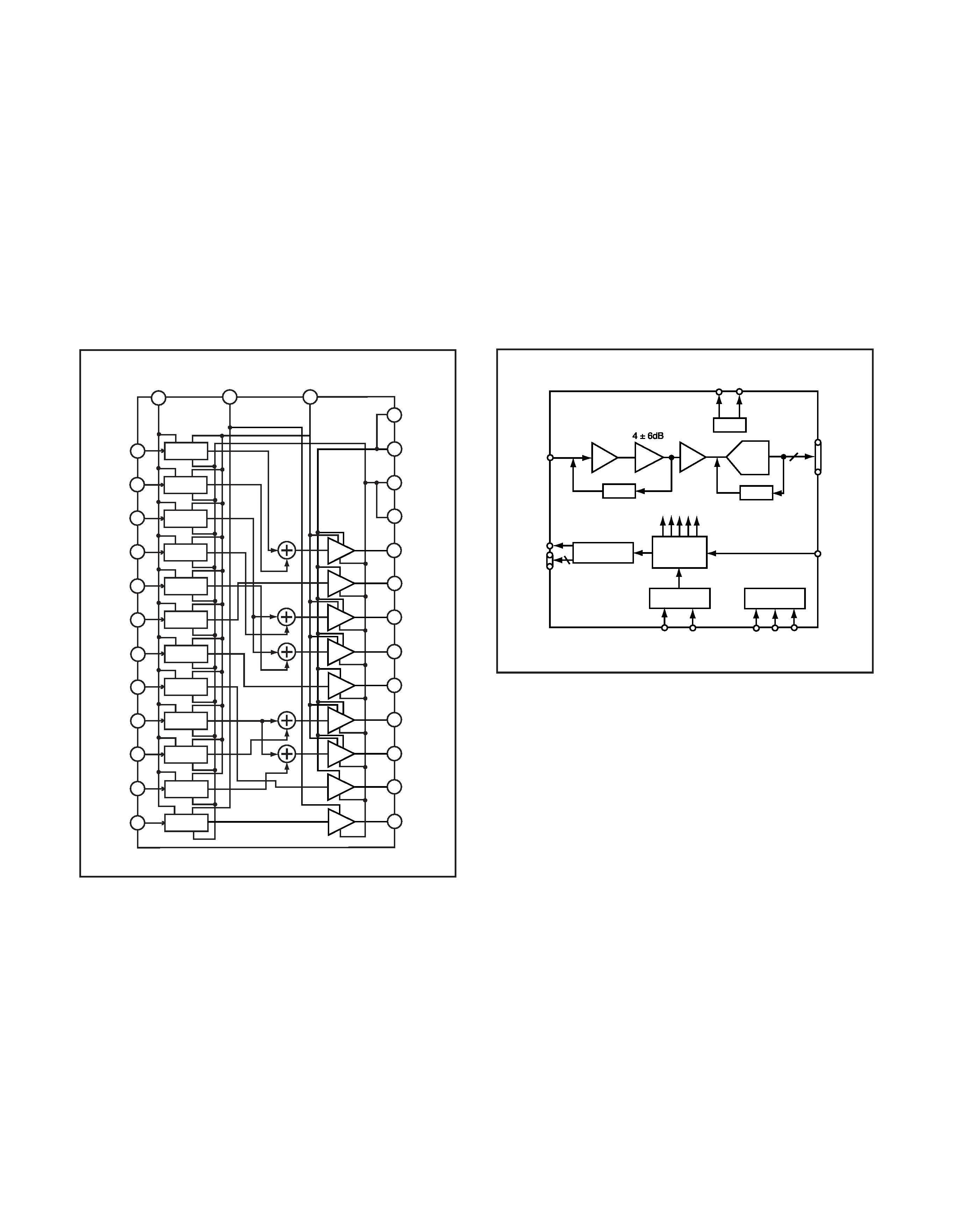
3. Part of IC906 (H Driver) and IC901 (V Driver)
An H driver (part of IC906) and V driver (IC901) are neces-
sary in order to generate the clocks (vertical transfer clock,
horizontal transfer clock and electronic shutter clock) which
driver the CCD.
IC906 has the generation of horizontal transfer clock and the
function of H driver, and is an inverter IC which drives the
horizontal CCDs (H1 and H2). In addition the XV1-XV4 sig-
nals which are output from IC101 are the vertical transfer
clocks, and the XSG signal which is output from IC101 is su-
perimposed onto XV1 and XV3 at IC901 in order to generate
a ternary pulse. In addition, the XSUB signal which is output
from IC101 is used as the sweep pulse for the electronic shut-
ter, and the RG signal which is output from IC906 is the reset
gate clock.
Fig. 1-4. IC906 Block Diagram
4. IC906 (H Driver, CDS, AGC and A/D converter)
IC906 contains the functions of H driver, CDS, AGC and A/D
converter. As horizontal clock driver for CCD image sensor,
HØ1 (A and B) and HØ2 (A and B) are generated inside, and
output to CCD.
The video signal which is output from the CCD is input to pins
(27) of IC906. There are sampling hold blocks generated from
the SHP and SHD pulses, and it is here that CDS (correlated
double sampling) is carried out.
After passing through the CDS circuit, the signal passes
through the AGC amplifier (VGA: Variable Gain Amplifier). It
is A/D converted internally into a 10-bit signal, and is then
input to ASIC (IC101). The gain of the VGA amplifier is con-
trolled by pin (31)-(33) serial signal which is output from ASIC
(IC101).
CCDIN
RG
H1-H4
VD
HD
SDATA
SCK
SL
CLI
DOUT
VRB
VRT
PRECISION
TIMING
CORE
SYNC
GENERATOR
PxGA
VGA
ADC
10
2~36 dB
VREF
CLAMP
INTERNAL
REGISTERS
INTERNAL
CLOCKS
CDS
CLAMP
HORIZONTAL
DRIVERS
4
Fig. 1-3. IC901 Block Diagram
20
21
22
23
24
25
27
28
1
2
3
9
10
11
12
13
14
15
16
6
18
17
7
IV1
CH1
IV3
CH2
CH3
IV2
IV6
IV5
CH4
CH5
ISUB
OV6
OV8
OV7
OV4
OV5
OV3
OV2
OV1
VL
VL
VM
VM
Level
conversion
26
IV4
8 OSUB
19
VDC
VDC
VL
VHH
Level
conversion
Level
conversion
Level
conversion
VL
VL
VH
VL
VH
VDC
VDC
VL
VH
VDC
Level
conversion
VL
VH
VDC
Level
conversion
VL
VH
VDC
Level
conversion
VL
VH
VDC
Level
conversion
VL
VH
VDC
Level
conversion
VL
VH
VDC
Level
conversion
VL
VH
VDC
Level
conversion
VL
VH
VDC
Level
conversion
VH
VDC
VHH
VL
2-level
VL
VM
VH
VL
VM
VH
VL
VM
VL
VM
VH
VL
VM
VH
VL
VM
VL
VM
VH
VL
VM
2-level
3-level
3-level
2-level
3-level
3-level
2-level
4
VH
5
VHH
VL
3-level
5. Lens drive block
5-1. Shutter drive
The shutter drive signal (SIN1 and SIN2) which is output from
the ASIC expansion port (IC106) is drived the shutter constant
level driver (IC951), and then shutter plunger is opened and
closed.
5-2. Iris drive
The iris stepping motor drive signals (IIN1 and IIN2) which are
output from the ASIC (IC101) are used to drive by the motor
driver (IC951).
5-3. Focus drive
The focus stepping motor drive signals (FIN1, FIN2, FIN3 and
FIN4) which are output from the ASIC (IC101) are used to
drive by the motor driver (IC951). Detection of the standard
focusing positions is carried out by means of the
photointerruptor (FPI-E) inside the lens block.
5-4. Zoom drive
The zoom DC motor drive signals (ZIN1 and ZIN2) which are
output from the ASIC (IC101) are used to drive by the motor
driver (IC951). Detection of the zoom positions is carried out
by means of photoreflector (ZPI-E) inside the lens block.

4
6. Circuit description
6-1. Digital clamp
The optical black section of the CCD extracts averaged val-
ues from the subsequent data to make the black level of the
CCD output data uniform for each line. The optical black sec-
tion of the CCD averaged value for each line is taken as the
sum of the value for the previous line multiplied by the coeffi-
cient k and the value for the current line multiplied by the
coefficient (k-1).
6-2. Signal processor
1.
correction circuit
This circuit performs (gamma) correction in order to maintain
a linear relationship between the light input to the camera
and the light output from the picture screen.
2. Color generation circuit
This circuit converts the CCD data into RGB signals.
3. Matrix circuit
This circuit generates the Y signals, R-Y signals and B-Y sig-
nals from the RGB signals.
4. Horizontal and vertical aperture circuit
This circuit is used gemerate the aperture signal.
6-3. AE/AWB and AF computing circuit
The AE/AWB carries out computation based on a 256-seg-
ment screen, and the AF carries out computations based on
a 11-segment screen.
6-4. SDRAM controller
This circuit outputs address, RAS, CAS and AS data for con-
trolling the SDRAM. It also refreshes the SDRAM.
6-5. Communication control
1. SIO
This is the interface for the 8-bit microprocessor.
2. PIO/PWM/SIO for LCD
8-bit parallel input and output makes it possible to switch be-
tween individual input/output and PWM input/output. It is pre-
pared for 16-bit parallel output.
6-6. TG/SG
Timing generated for 4 million pixel CCD control.
6-7. Digital encorder
It generates chroma signal from color difference signal.
6-8. JPEG encorder and decorder
It is compressed and elongated the data by JPEG system.
7. Outline of Operation
When the shutter opens, the reset signals and the serial sig-
nals ("take a picture" commands) from the 8-bit microproces-
sor are input to ASIC (IC101) and operation starts. When the
TG/SG drives the CCD, picture data passes through the A/D
and CDS, and is then input to the ASIC as 12-bit data. The
AF, AE, AWB, shutter, and AGC value are computed from this
data, and three exposures are made to obtain the optimum
picture. The data which has already been stored in the SDRAM
is read by the CPU and color generation is carried out. Each
pixel is interpolated from the surrounding data as being ei-
ther R, G and B primary color data to produce R, G and B
data. At this time, correction of the lens distortion which is a
characteristic of wide-angle lenses is carried out. After AWB
and
processing are carried out, a matrix is generated and
aperture correction is carried out for the Y signal, and the
data is then compressed by the JPEG method by (JPEG) and
is then written to card memory (SD card).
When the data is to be output to an external device, it is taken
data from the memory and output via the USB. When played
back on the LCD and monitor, data is transferred from memery
to the SDRAM, and the data elongated by JPEG decorder is
displayed over the SDRAM display area.
8. LCD Block
LCD block is in the CP1 board, and it is constructed by VCOM
generation circuit etc.
The video signal from the ASIC are 6-bit digital signal, and
input to LCD directly. It is converted into RGB signals at driver
circuit in the LCD.
The VCOM (common polar voltage: AC) and the R, G and B
signals becomes greater, the display becomes darker; if the
difference in potential is smaller, the element opens and the
LCD become brighter. And also the timing pulse except the
video signal is input to LCD directly from ASIC.

5
1-2. CP1 POWER CIRCUIT DESCRIPTION
1. Outline
This is the main power circuit, and is comprised of the follow-
ing blocks.
Switching controller (IC501)
Analog system power output (T5001, Q5001, IC502)
Digital 3.25 V power output (L5004)
Digital 1.7 V power output (L5005)
5 V system power output (L5003, Q5009)
LCD 15 V system power output (L5001, Q5002)
Backlight power output (L5002)
Motor system power output (IC955, L9551, Q9551)
2. Switching Controller (IC501)
This is the basic circuit which is necessary for controlling the
power supply for a PWM-type switching regulator, and is pro-
vided with seven built-in channels, only CH2 (digital 3.25 V),
CH3 (digital 1.7 V), CH4 (digital system), CH5 (analog sys-
tem), CH6 (LCD system) and CH7 (backlight sysetm) are used.
Feedback from 3.25 V (D) (CH2), 1.7 V (D) (CH3), digital sys-
tem (CH4), analog system (CH5), LCD system (CH6) and
backlight system (CH7) power supply outputs are received,
and the PWM duty is varied so that each one is maintained at
the correct voltage setting level.
Feedback for the backlight power (CH7) is provided to the
both ends voltage of registance so that regular current can
be controlled to be current that was setting.
2-1. Short-circuit Protection Circuit
If output is short-circuited for the length of time setting inside
(Pin (42) of IC501), all output is turned off. The control signal
(P ON) are recontrolled to restore output.
3. Analog System Power Output
+12 V (A), +3.45 V (A) and -8.0 V (A) are output. Feedback for
the 13 V (+12 V (A)) is provided to the switching controller
(Pin (53) of IC501) so that PWM control can be carried out.
+3.45 V (A) is output which dropped 3.4 V by 5V system power
output at regulator IC502.
4. Digital 3.25 V Power Output
+3.25 V (D) is output. Feedback for the +3.25 V (D) is pro-
vided to the switching controller (Pins (32) of IC501) so that
PWM control can be carried out.
5. Digital 1.7 V Power Output
+1.7 V (D) is output. Feedback for the +1.7 V (D) is provided
to the swiching controller (Pin (31) of IC501) so that PWM
control can be carried out.
6. 5 V System Power Output
+5 V is output. Feedback for the +5 V is provided to the
swiching controller (Pin (52) of IC501) so that PWM control
can be carried out.
7. LCD System Power Output
+15 V (L) and 5 V (L) are output. Feedback for the +15 V (L) is
provided to the swiching controller (Pin (56) of IC501) so that
PWM control can be carried out.
8. Backlight Power Output
Regular current is being transmitted to LED for LCD back-
light. Feedback for the both ends voltage of registance that is
being positioned to in series LED are provided to the switch-
ing controller (Pin (48) of IC501) so that PWM control to be
carried out.
9. Motor System Power Output
3.7 V is output. Feedback for the 3.7 V is provided to (Pin (1)
of IC955) so that PWM control can be carried out.