ORDER NO.
PIONEER CORPORATION 4-1, Meguro 1-chome, Meguro-ku, Tokyo 153-8654, Japan
PIONEER ELECTRONICS (USA) INC. P.O. Box 1760, Long Beach, CA 90801-1760, U.S.A.
PIONEER EUROPE NV Haven 1087, Keetberglaan 1, 9120 Melsele, Belgium
PIONEER ELECTRONICS ASIACENTRE PTE. LTD. 253 Alexandra Road, #04-01, Singapore 159936
PIONEER CORPORATION 2007
RRV3576
T ZZK APR. 2007 Printed in Japan
DVD/CD RECEIVER
XV-DV88
THIS MANUAL IS APPLICABLE TO THE FOLLOWING MODEL(S) AND TYPE(S).
Model No.
Order No.
Remarks
XV-HTD540/KUCXJ
RRV2908
¶ This service manual should be used together with the following manual(s):
¶ For SPECIFICATIONS and PANEL FACILITIES, refer to the operating instructions.
Model
Type
Power Requirement
Region No.
The voltage can be converted by
the following method.
XV-DV88
DDRXJ
AC 110 V to 127 V/220 V to 230 V/240 V
4
With the voltage selector
XV-DV88
DDXJ/RB
AC 110 V to 127 V/220 V to 230 V/240 V
2
With the voltage selector
XV-DV88
DDXJ/RA
AC 110 V to 127 V/220 V to 230 V/240 V
1
With the voltage selector
XV-DV88
DPWXJ
AC 110 V to 127 V/220 V to 230 V/240 V
4
With the voltage selector
2
1
23
4
12
3
4
C
D
F
A
B
E
XV-DV88
This service manual is intended for qualified service technicians ; it is not meant for the casual do-
it-yourselfer. Qualified technicians have the necessary test equipment and tools, and have been
trained to properly and safely repair complex products such as those covered by this
manual.Improperly performed repairs can adversely affect the safety and reliability of the product
and may void the warranty. If you are not qualified to perform the repair of this product properly and
safely, you should not risk trying to do so and refer the repair to a qualified service technician.
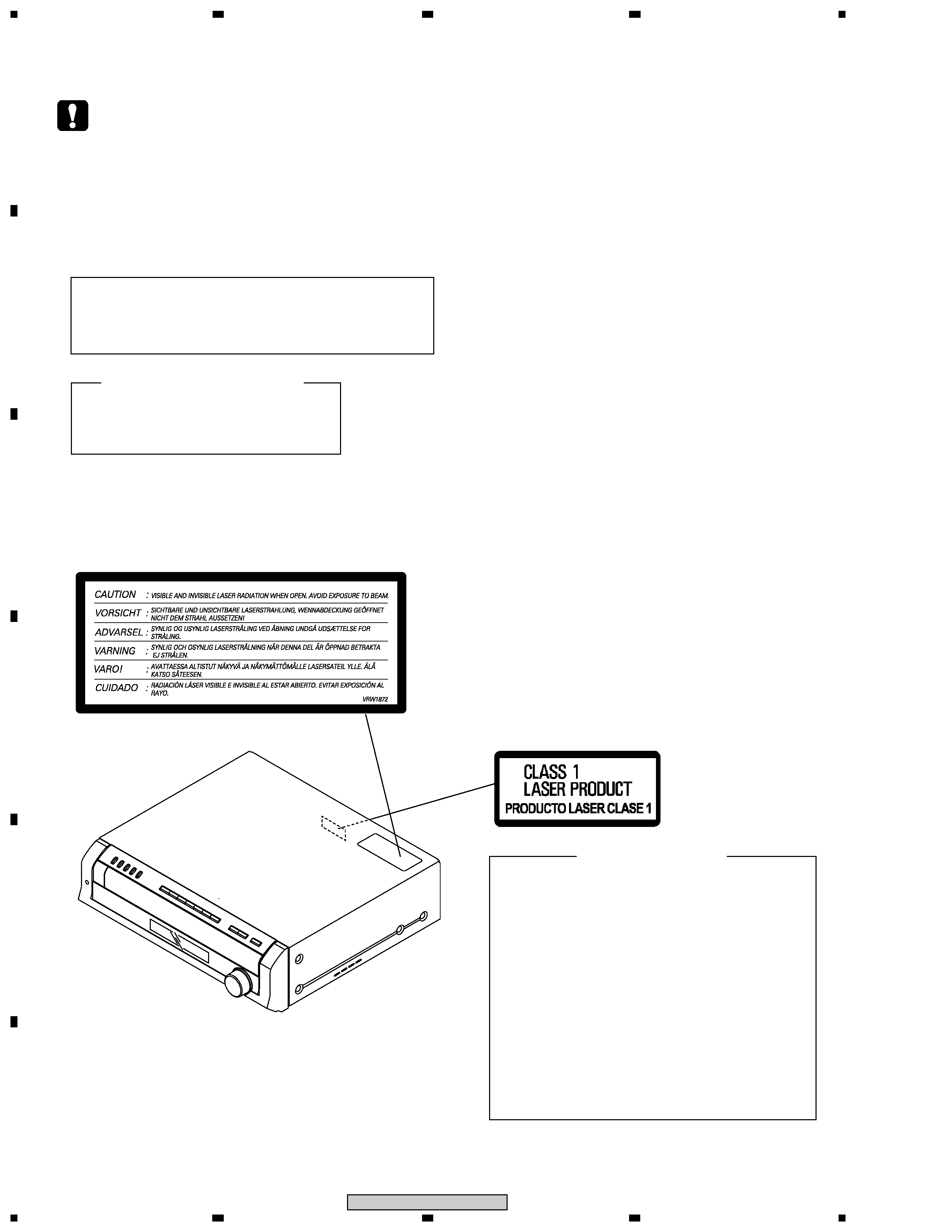
LABEL CHECK
: Refer to page 87 on the service manual RRV2908.
LASER DIODE CHARACTERISTICS
FOR DVD : MAXIMUM OUTPUT POWER : 5 mW
WAVELENGTH : 655 nm
FOR CD : MAXIMUM OUTPUT POWER : 5mW
WAVELENGTH : 785 nm
Additional Laser Caution
1. Inside detection switch (the SSIB assy) and clamp-status
detection switch (S11 on the TRSB assy) are detected by
the microprocessor (IC601 in the DVDM assy).
· To permit the laser diode to oscillate, it is required to set the
inside detection switch for the inside position (ON) and to
set the loading-status detection switch for the clamp position
(the center terminal of S11 is shorted to +5V). The 655 nm
laser diode for DVD oscillation will continue if pin 89 of IC301
is shorted to +5V (fault condition) in the DVDM assy.
The 785 nm laser diode for CD oscillates if pin 90 of IC301 is
shorted to +5V in the DVDM assy.
In the test mode
, the laser diode oscillates when micro-
processor detects a PLAY signal, or when the PLAY key is
pressed (S5857 ON in the FUNC KEY assy), with the above
requirements satisfied.
2. When the cover is open, close viewing through the objective
lens with the naked eye will cause exposure to the laser beam.
Printed on the Rear Panel
VRW1872
WARNING!
The laser component is capable of emitting radiation exceeding
the limit for CLASS 1. A specially instructed person should do
servicing operation of the apparatus.
SAFETY INFORMATION
3
1
23
4
1
2
3
4
C
D
F
A
B
E
XV-DV88
Ref.
Part No.
No.
Mark
Symbol and Description
XV-DV8
XV-DV88
XV-DV88
XV-DV88
XV-DV88
Remarks
/DDXJ/RA
/DDRXJ
/DDXJ/RB
/DDXJ/RA
/DPWXJ
< PCB ASSEMBLIES >
NSP
MAIN ASSY
XWM3232
XWM3232
XWM3266
XWM3232
XWM3232
P9- 7
AF ASSY
XWZ3836
XWZ3836
XWZ3897
XWZ3836
XWZ3836
< PACKING SECTION >
P7- 1
AC Power Cord
ADG1154
ADG1158
ADG1158
ADG1154
ADG7099
AC Power Cord
Not used
XDG3009
Not used
Not used
Not used
P7- 5
NSP
Dry Cell Battery (R6P/AA)
VEM1031
XEX3002
XEX3002
XEX3002
XEX3002
P7- 8
Operating instructions (English)
XRB3045
XRB3077
XRB3040
XRB3077
XRB3077
P7- 9
Operating instructions (Spanish)
Not used
XRC3124
Not used
Not used
Not used
P7- 9
Operating instructions (Arabic)
Not used
Not used
XRC3126
Not used
Not used
P7-10
NSP
Warranty Card
ARY7025
Not used
Not used
ARY7025
ARY7047
P7-15
Packing Case
XHD3452
XHD3755
XHD3755
XHD3757
XHD3756
P7-16
Power Plug Adapter
XKM3001
XKM3002
Not used
XKM3001
Not used
Caution Sheet AR
Not used
XRH3002
Not used
Not used
Not used
< EXTERIOR SECTION >
P9-22
Rear Panel
XNC3273
XNC3533
XNC3534
XNC3536
XNC3535
P9-39
NSP
Tray Cap Assy
XXG3174
XXG3173
XXG3173
XXG3173
XXG3173
P9-41
Tray Cap
XAK3449
XAK3459
XAK3459
XAK3459
XAK3459
P9-42
Bonnet HTM
XZN3166
XZN3195
XZN3195
XZN3195
XZN3195
P9-44
NSP
Energy Star Label
Not used
Not used
Not used
Not used
AAX8022
NSP
Pop Label
XAX3431
Not used
Not used
Not used
Not used
NSP
Region Label
Not used
Not used
XAX3649
Not used
Not used
NSP
DF Label
AAX7960
Not used
Not used
AAX7960
Not used
< FRONT PANEL SECTION >
P11- 5
NSP
Front Panel Assy
XXG3177
XXG3301
XXG3301
XXG3301
XXG3301
P11- 6
Top Panel Assy
XZN3147
XZN3146
XZN3146
XZN3146
XZN3146
P11- 7
Display Window
XAK3447
XAK3570
XAK3570
XAK3570
XAK3570
P11- 8
Power Cap
XAK3445
XAK3460
XAK3460
XAK3460
XAK3460
P11- 9
Front Panel
XMB3156
XMB3150
XMB3150
XMB3150
XMB3150
P11-10
FL Filter HTM
AAK8100
AAK8390
AAK8390
AAK8390
AAK8390
P11-19
MIC Knob
XAA3024
XAA3029
XAA3029
XAA3029
XAA3029
CONTRAST TABLE
XV-DV88/DDRXJ, /DDXJ/RB, /DDXJ/RA, /DPWXJ and XV-DV8/DDXJ/RA are constructed the same except for the following :
1. CONTRAST OF MISCELLANEOUS PARTS
jp
f
y
For the applying amount of lubricants or glue, follow the instructions in this manual.
(In the case of no amount instructions, apply as you think it appropriate.)
Parts marked by "NSP" are generally unavailable because they are not in our Master Spare Parts List.
The
mark found on some component parts indicates the importance of the safety factor of the part.
Therefore, when replacing, be sure to use parts of identical designation.
Screws adjacent to
mark on product are used for disassembly.
Reference Nos. indicate the pages and Nos. in the service manual for the base model.
NOTES:
·When ordering resistors, first convert resistance values into code form as shown in the following examples.
Ex.1 When there are 2 effective digits (any digit apart from 0), such as 560 ohm and 47k ohm (tolerance is shown by J=5%,
and K=10%).
560
56
× 101
561 ........................................................ RD1/4PU 5 6 1 J
47k
47
× 103
473 ........................................................ RD1/4PU 4 7 3 J
0.5
R50 ..................................................................................... RN2H R 5 0 K
1
1R0 ..................................................................................... RS1P 1 R 0 K
Ex.2 When there are 3 effective digits (such as in high precision metal film resistors).
5.62k
562
× 101
5621 ...................................................... RN1/4PC 5 6 2 1 F
Notes : For PCB ASSEMBLIES, Refer to "
CONTRAST OF PCB ASSEMBLIES" .
4
1
23
4
12
3
4
C
D
F
A
B
E
XV-DV88
CONTRAST OF PCB ASSEMBLIES
Mark
Symbol and Description
Part No.
Remarks
XWZ3836
XWZ3897
R5532
RS1/16S473J
RS1/16S393J
R5539
RS1/16S473J
RS1/16S683J
F
D AF ASSY
XWZ3897 and XWZ3836 are constructed the same except for the following :