ORDER NO.
PIONEER CORPORATION 4-1, Meguro 1-chome, Meguro-ku, Tokyo 153-8654, Japan
PIONEER ELECTRONICS SERVICE, INC. P.O. Box 1760, Long Beach, CA 90801-1760, U.S.A.
PIONEER EUROPE NV Haven 1087, Keetberglaan 1, 9120 Melsele, Belgium
PIONEER ELECTRONICS ASIACENTRE PTE. LTD. 253 Alexandra Road, #04-01, Singapore 159936
PIONEER CORPORATION 2001
c
XR-MT3V
RRV2436
T ZZK MAR. 2001 Printed in Japan
STEREO CD/VCD RECEIVER
1. SAFETY INFORMATION ....................................... 2
2. EXPLODED VIEWS AND PARTS LIST ................. 3
3. BLOCK DIAGRAM AND SCHEMATIC DIAGRAM ..... 8
4. PCB CONNECTION DIAGRAM ........................... 22
5. PCB PARTS LIST ................................................ 32
6. ADJUSTMENT ..................................................... 35
CONTENTS
7. GENERAL INFORMATION ................................ 36
7.1 DIAGNOSIS .................................................. 36
7.1.1 TROUBLE SHOOTING ........................ 36
7.1.2 SEQUENCE AFTER THE POWER
IS TURNED ON ................................... 39
7.1.3 DISASSEMBLY/ASSEMBLY ................ 40
7.2 PARTS .......................................................... 48
7.2.1 IC .......................................................... 48
7.2.2 DISPLAY ............................................... 51
7.3 REMOTE CONTROL UNIT .......................... 52
8. PANEL FACILITIES AND SPECIFICATIONS .... 54
Type
Model
Power Requirement
The voltage can be converted by
XR-MT3V
the following method.
DDXCN
AC110-127V/220-230V/240V
With the voltage selector
ULXCN/NC
AC230-240V
THIS MANUAL IS APPLICABLE TO THE FOLLOWING MODEL(S) AND TYPE(S).
Component
Model
Service manual
Remarks
STEREO Video CD RECEIVER SYSTEM
X-MT4000
RRV2369
DDXCN type
ULXCN/NC type
STEREO CD/VCD RECEIVER
XR-MT3V
XR-MT3V
RRV2436
This manual
SPEAKER SYSTEM
S-MT3V
S-MT3V-N
RRV2437
¶ System Component Table
XR-MT3V
2
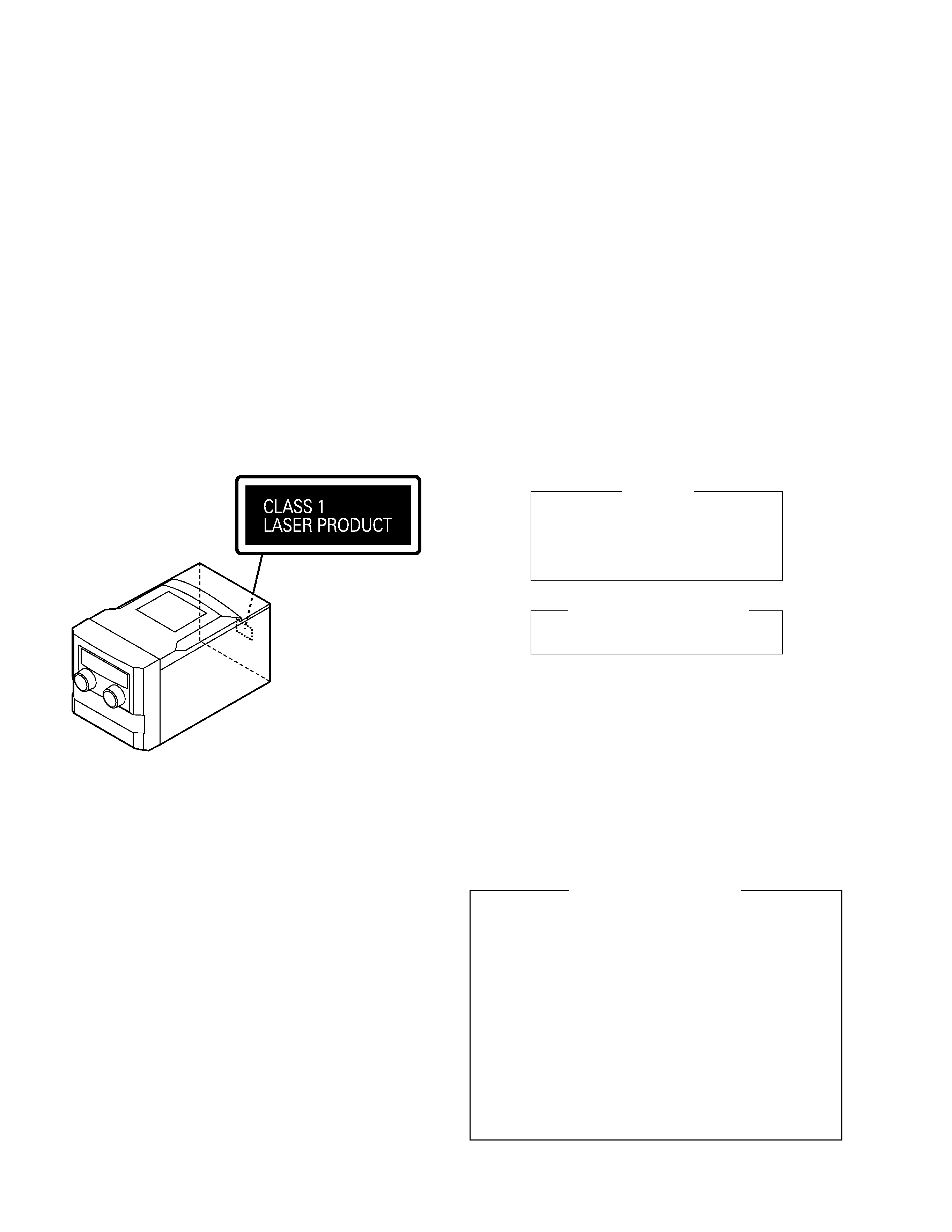
Additional Laser Caution
1. Laser Interlock Mechanism
The position of the switch for detecting loading state is
detected by the system microprocessor, and the design
prevents laser diode oscillation when the switch is pressed
physically.
Thus, the interlock will no longer function if the switch is released
physically and deliberatery.
Laser diode oscillation will continue, if pin 46 of TA2065F (IC2)
on the CD SERVO PCB ASSY is connected to GND, or else
the terminals of Q1 are shorted to each other (fault condition).
2. When the cover is opened, close viewing of the objective
lens with the naked eye will cause exposure to a Class 1
laser beam.
LASER DIODE CHARACTERISTICS
MAXIMUM OUTPUT POWER: 5 mW
WAVELENGTH: 760 - 800 nm
IMPORTANT
THIS PIONEER APPARATUS CONTAINS
LASER OF CLASS 1.
SERVICING OPERATION OF THE APPARATUS
SHOULD BE DONE BY A SPECIALLY
INSTRUCTED PERSON.
LABEL CHECK (For ULXCN/NC Type)
1. SAFETY INFORMATION
This service manual is intended for qualified service technicians ; it is not meant for the casual do-it-
yourselfer. Qualified technicians have the necessary test equipment and tools, and have been trained
to properly and safely repair complex products such as those covered by this manual.
Improperly performed repairs can adversely affect the safety and reliability of the product and may
void the warranty. If you are not qualified to perform the repair of this product properly and safely, you
should not risk trying to do so and refer the repair to a qualified service technician.
3
XR-MT3V
97
98
G
F
E
B
J
D
C
D
C
A
I
H
G
E
F
K
K
H
A
B
I
J
L
8
34
87
54
5
27
7
2
7
15
64
32
20
8
44
28
31
8
56
15
51
59
9
1
8
2
2
8
14
49
8
3
53
2
8
18(2/2)
6
15
50
62
62
3
15
6
2
4
8
3
48
35
37
8
47
12
8
58
77
9
8
75
74
46
13
8
76
19
3
9
73
80
45
79
81
82
17
60
8
41
10
40
85
52
Refer to section
"2.2 CD MECHA.
SECTION".
6
6
39
18(1/2)
26,61
29
8
8
3
36
70
89
100
65
65
84
5 16
44
93
22
2
99
4
4
55
91
92
94
6
96
21
67
24
42
43
23
L
M
95
8
78
90
25
38
88
63
E
A
G
11
H
F
B
E
C
D
33
N
M
N
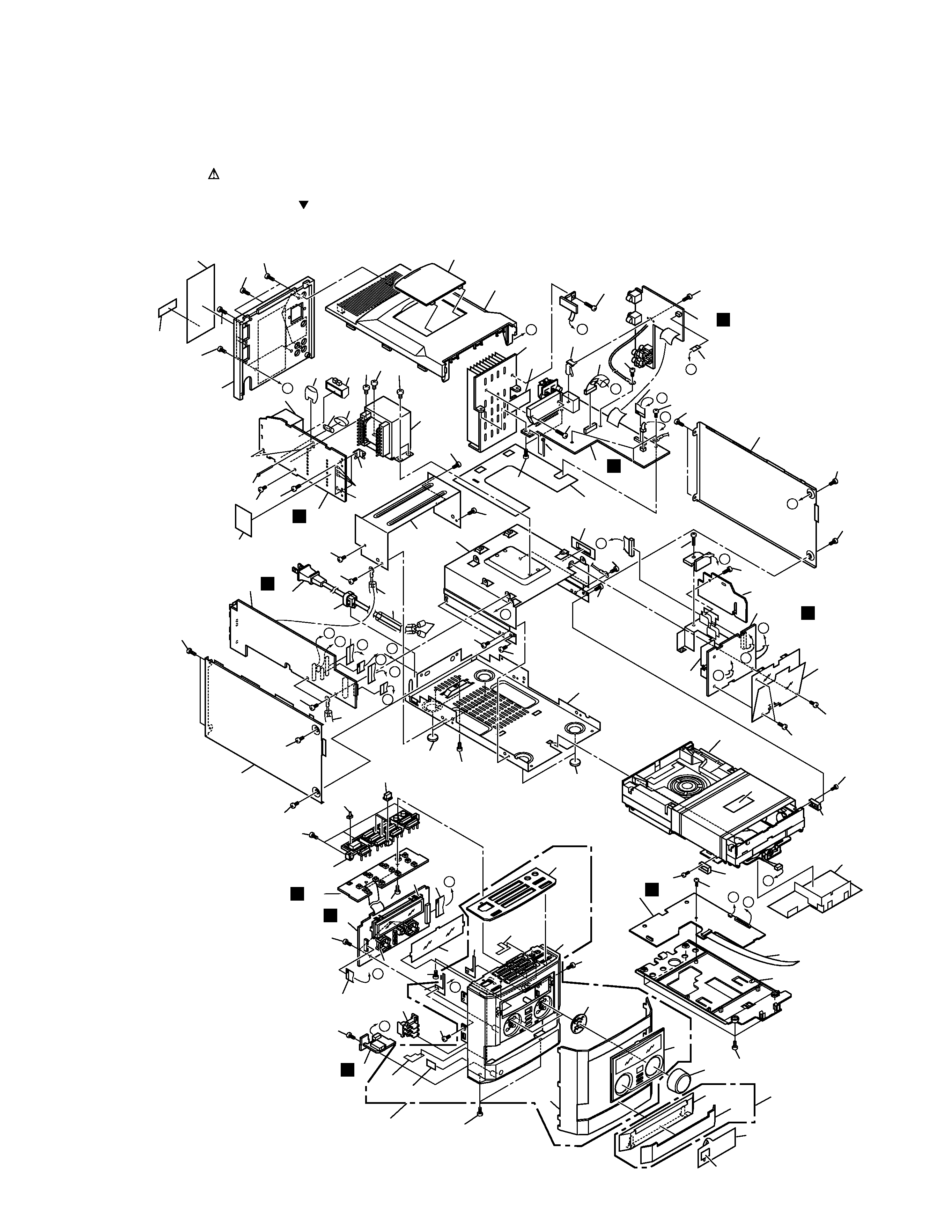
2. EXPLODED VIEWS AND PARTS LIST
NOTES:
· Parts marked by "NSP" are generally unavailable because they are not in our Master Spare Parts List.
· The mark found on some component parts indicates the importance of the safety factor of the part.
Therefore, when replacing, be sure to use parts of identical designation.
· Screws adjacent to mark on the product are used for disassembly.
2.1 EXTERIOR SECTION

4
XR-MT3V
(1) EXTERIOR SECTION PARTS LIST
Mark No.
Description
Part No.
1
AUDIO Assy
AUD-PMT2E
2
Screw
BBZ30P060FMC
3
Screw
KBZ30P060FNI
4
Screw
BBZ30P140FMC
5
Screw
BBZ40P060FMC
6
Screw
BPZ20P050FMC
7
Screw
BPZ26P080FMC
8
Screw
BPZ30P100FNI
9
Screw
CBZ30P060FMC
10
MT VCD UNIT
CD--PMT2E
NSP
11
CONTROL & DISPLAY Assy CTL-PMT1E
12
DISPLAY CONTROL Assy
DIP-PMT2E-DL
NSP
13
HP JACK PCB Assy
· · · · · ·
14
JACK Assy
JK--PMT2E
15
Screw
KBZ30P040FMC
16
Screw
BBZ40P080FMC
17
CD DOOR Assy MT
SUBPMT1DR01
18
POWER PCB Assy
See Contrast table(2)
19
Front Panel Assy
SUBPMT2FP03
20
STD. TUNER Assy
TUN-PMT2E
21
FFC Cable 16Pin
040160100101
22
FFC Cable 16Pin
040160260100
23
FFC Cable 17Pin
040170100100
24
FFC Cable 24Pin
040240200130
25
FFC Cable 35Pin
040350410100
26
Power TF EI35 11-2
1231D3513140
27
Power Transformer
1235D4000130
28
Protector (4A)
AEK7018
29
Fuse #2181.25 (1.25A/250V) 124-012520-007
30
· · · · · ·
31
Protector (630mA)
AEK7006
32
PLA-VDE-6'06"-VDG
See Contrast table(2)
32
PLA-ULN-6'&&&-VDE-MG
See Contrast table(2)
33
CD MECHA,CMCJ
153000117000
34
Top Panel
See Contrast table(2)
35
Direct Access Knob Lens
500PMT111000
36
Back Cover
500PMT182000
37
Power Standby Lens
500PMT129000
38
Fuse Insulation Cap
500623200000
39
CD Base Adaptor R
503PMT125000
40
CD Base Adaptor L
503PMT126000
41
Servo PCB Bracket
505PMT114000
42
FL Bracket
505PMT134000
43
LED Bracket
505PMT135000
44
PCB Mounting Bracket
505PMT136000
45
Volume Knob
510PMT103001
46
Clock Control Knob Set
510PMT108001
47
Direct Access Knob Set
510PMT109010
48
Side Panel-L
600PMT117001
49
Side Panel-R
600PMT118001
NSP
50
Bottom Tray
600PMT121000
51
Transformer Bracket
605PMT122000
52
FFC Cable HLD
605PMT172000
53
Cable Holder
605PMT143000
54
Power Heat Sink
613PMT168000
55
Heat Sink
613PMT159000
56
CD Shield Plate
650PMT139000
57
· · · · · ·
58
Display Filter Plate
650PMT147002
59
PC Sheet
650PMT149000
60
Transport Stopper PL
650PMT197010
61
Shielding Plate
650277225000
62
Rubber Foot
700PMT130000
63
Capacitor Boot
700PMT150000
64
Bushing
700PMT156000
65
Cable/Plastic Tie
727000100000
66
· · · · · ·
NSP
67
Trans. Stopper Label
809PMT194021
68
· · · · · ·
69
· · · · · ·
70
Spec Label
See Contrast table(2)
71
· · · · · ·
72
· · · · · ·
NSP
73
Front Panel
500PMT101001
NSP
74
GND. Copper Plate C
650PMT152000
NSP
75
GND. Copper Plate D
650PMT153000
NSP
76
GND. Copper Plate E
650PMT155000
NSP
77
Control Panel Plate
650PMT116010
NSP
78
Front Cover
600PMT119030
NSP
79
Display Lens
500PMT106010
NSP
80
Illuminated Ring
509PMT105000
NSP
81
CD Door
500PMT102001
NSP
82
CD Door Cover
600PMT120010
83
· · · · · ·
84
PCB Insulation Sheet
650PMT157000
85
CD Caution Label
809PMT194070
86
· · · · · ·
87
Voltage Sel. Cover
See Contrast table(2)
88
Voltage Sel. Knob
See Contrast table(2)
NSP
89
Serial Label
809000009000
90
Tube AWG5 D4.72 L70
728000047L07
91
Tube AWG5 D4.72 L90
728000047L09
92
Tube AWG1 D7.35 L120
728000073L12
93
Tube AWG1 D7.35 L160
728000073L16
94
Tube AWG1 D7.35 L15
728000073L15
95
FFC Cable 3Pin
040030190100
96
Shielding Sheet
650PMT171000
97
GND Copper Plate A
650PMT140000
98
GND Copper Plate B
650PMT141000
99
GUARD PCB
03300PMT2102
100
Mica Plate
650PMT161000
Mark No.
Description
Part No.

5
XR-MT3V
(2) CONTRAST TABLE
XR-MT3V/DDXCN and ULXCN/NC are constructed the same except for the following :
Part No.
Mark No.
Symbol and Description
XR-MT3V
XR-MT3V
Remarks
DDXCN
ULXCN/NC
18
POWER PCB Assy
SUBRTFPMT2EDB
RTF-PMT2E-DL
32
PLA-VDE-6'06"-VDG
Not used
134220120001
32
PLA-ULN-6'&&&-VDE-MG
134250220000
Not used
34
Top Panel
500PMT167001
500PMT170001
70
Spec Label
809PMT296010
809PMT296020
87
Voltage Sel. Cover
500PMT110001
Not used
88
Voltage Sel. Knob
510PMT169001
Not used