ORDER NO.
PIONEER ELECTRONIC CORPORATION 4-1, Meguro 1-Chome, Meguro-ku, Tokyo 153-8654, Japan
PIONEER ELECTRONICS SERVICE, INC. P.O. Box 1760, Long Beach, CA 90801-1760, U.S.A.
PIONEER ELECTRONIC (EUROPE) N.V. Haven 1087, Keetberglaan 1, 9120 Melsele, Belgium
PIONEER ELECTRONICS ASIACENTRE PTE. LTD. 501 Orchard Road, #10-00 Wheelock Place, Singapore 238880
PIONEER ELECTRONIC CORPORATION 1998
RRV1995
T ZZW AUG. 1998 Printed in Japan
CONTENTS
1. CONTRAST OF MISCELLANEOUS PARTS ........ 2
2. SCHEMATIC DIAGRAM ....................................... 4
3. PCB CONNECTION DIAGRAM .......................... 10
4. ADJUSTMENT .................................................... 11
¶ Refer to the service manual RRV2006 for XR-A660/DLXJ/NC.
THIS MANUAL IS APPLICABLE TO THE FOLLOWING MODEL(S) AND TYPE(S).
Model
XR-A660SW
Type
Power Requirement
The voltage can be converted by
the following method.
DDXJ
MLWXJ/EE
STEREO CD CASSETTE DECK RECEIVER
XR-A660SW
XR-A660EE
AC110V127V/220230V/240V
With the voltage selector
AC220230V
XR-A660EE
XR-A660SW, XR-A660EE
2
ASSEMBLIES
NSP
COMPLEX Assy
XWM3049
XWM3053
XWM3086
P7- 3
PRIMARY Assy
XWZ3048
XWZ3048
XWZ3056
P7- 29
SUB TRANS Assy
XWZ3049
XWZ3049
XWZ3155
P9- 1
DISPLAY Assy
XWZ3085
XWZ3095
XWZ3096
P7- 4
FM/AM TUNER MODULE
AXQ7065
AXQ7062
AXQ7069
PACKING SECTION
P3- 1
FM Antenna
ADH7004
ADH7004
ADH7011
P3- 2
Operating Instructions
XRE3009
Not used
Not used
(English/ Chinese/ Russian)
P3- 2
Operating Instructions
Not used
XRE3013
XRE3013
(English/ Arabian/ Russian)
P3- 10
Packing Case
XHD3032
XHD3042
XHD3043
P3- 13
Power Cord
ADG1154
ADG1158
ADG1154
SW Antenna
Not used
ADH7006
Not used
EXTERIOR(1/2) SECTION
P5- 7
Display Panel
XAK3020
XAK3020
XAK3058
NSP
Getter
XAX3066
XAX3066
XAX3096
EXTERIOR(2/2) SECTION
P7- 5
T1 Power Tranceformer
XTS3015
XTS3015
XTS3016
P7- 6
FU2, FU3 Fuse (T2A)
AEK1057
AEK1057
Not used
P7- 7
FU1 Fuse (T2A)
Not used
Not used
AEK1057
P7- 7
FU1 Fuse (T4A)
AEK1060
AEK1060
Not used
P7- 15
Rear Panel
XNC3001
XNC3001
XNC3021
P7- 25
Caution Label
PRW1018
Not used
Not used
P7- 26
NSP
Name Label
Not used
XAL3005
Not used
P7- 30
NSP
Fuse Card
AAX2357
AAX2357
Not used
P7- 31
Fuse Card
Not used
Not used
AAX7026
P7- 31
NSP
Fuse Card
AAX7099
AAX7099
Not used
1. CONTRAST OF MISCELLANEOUS PARTS
CONTRAST TABLE
XR-A660SW/DDXJ, XR-A660EE/MLWXJ/EE and XR-A660/DLXJ/NC are constructed the same except for the following :
Note:
÷ For ASSEMBLIES, refer to "CONTRAST OF PCB ASSEMBLIES", "2. SCHEMATIC DIAGRAM" and
"3. PCB CONNECTION DIAGRAM".
Part No.
XR-A660
/DLXJ/NC
Ref. No.
Symbol and Description
Remarks
Mark
XR-A660SW
/DDXJ
XR-A660EE
/MLWXJ/EE
NOTES:
·Parts marked by "NSP" and
can not be supplied.
·The mark found on some component parts indicates the importance of the safety factor of the part.
Therefore, when replacing, be sure to use parts of identical designation.
· Screws adjacent to mark on the product are used for disassembly.
·Reference Nos. indicate the pages and Nos. in the service manual for the base model.
·When ordering resistors, first convert resistance values into code form as shown in the following examples.
Ex.1 When there are 2 effective digits (any digit apart from 0), such as 560 ohm and 47k ohm (tolerance is shown by J=5%,
and K=10%).
560
56
× 101
561 ........................................................ RD1/4PU 5 6 1 J
47k
47
× 103
473 ........................................................ RD1/4PU 4 7 3 J
0.5
R50 ..................................................................................... RN2H R 5 0 K
1
1R0 ..................................................................................... RS1P 1 R 0 K
Ex.2 When there are 3 effective digits (such as in high precision metal film resistors).
5.62k
562
× 101
5621 ...................................................... RN1/4PC 5 6 2 1 F
XR-A660SW, XR-A660EE
3
C5501
Not used
Not used
CCSQCH220J50
C5502
Not used
Not used
CCSQCH270J50
C5815
Not used
Not used
CKSQYB103K50
D5594
Not used
1SS133
Not used
D5595
Not used
Not used
1SS133
R9996
RS1/10S0R0J
RS1/10S0R0J
RS1/10S561J
X5501 (6MHz)
RSS1050
RSS1050
ASS7015
CONTRAST OF PCB ASSEMBLIES
XWZ3056 and XWZ3048 are constructed the same except for the following :
PRIMARY ASSY
Part No.
XWZ3048
Mark
Symbol and Description
Remarks
XWZ3056
H3H6
Fuse Clip
AKR7001
Not used
S1
AKX7006
Not used
XWZ3095, XWZ3096 and XWZ3085 are constructed the same except for the following :
DISPLAY ASSY
Part No.
XWZ3085
Mark
Symbol and Description
Remarks
XWZ3095
XWZ3096
XWZ3155 and XWZ3049 are constructed the same except for the following :
SUB TRANS ASSY
Part No.
XWZ3049
Mark
Symbol and Description
Remarks
XWZ3155
S2
AKX7004
Not used
XR-A660SW, XR-A660EE
4
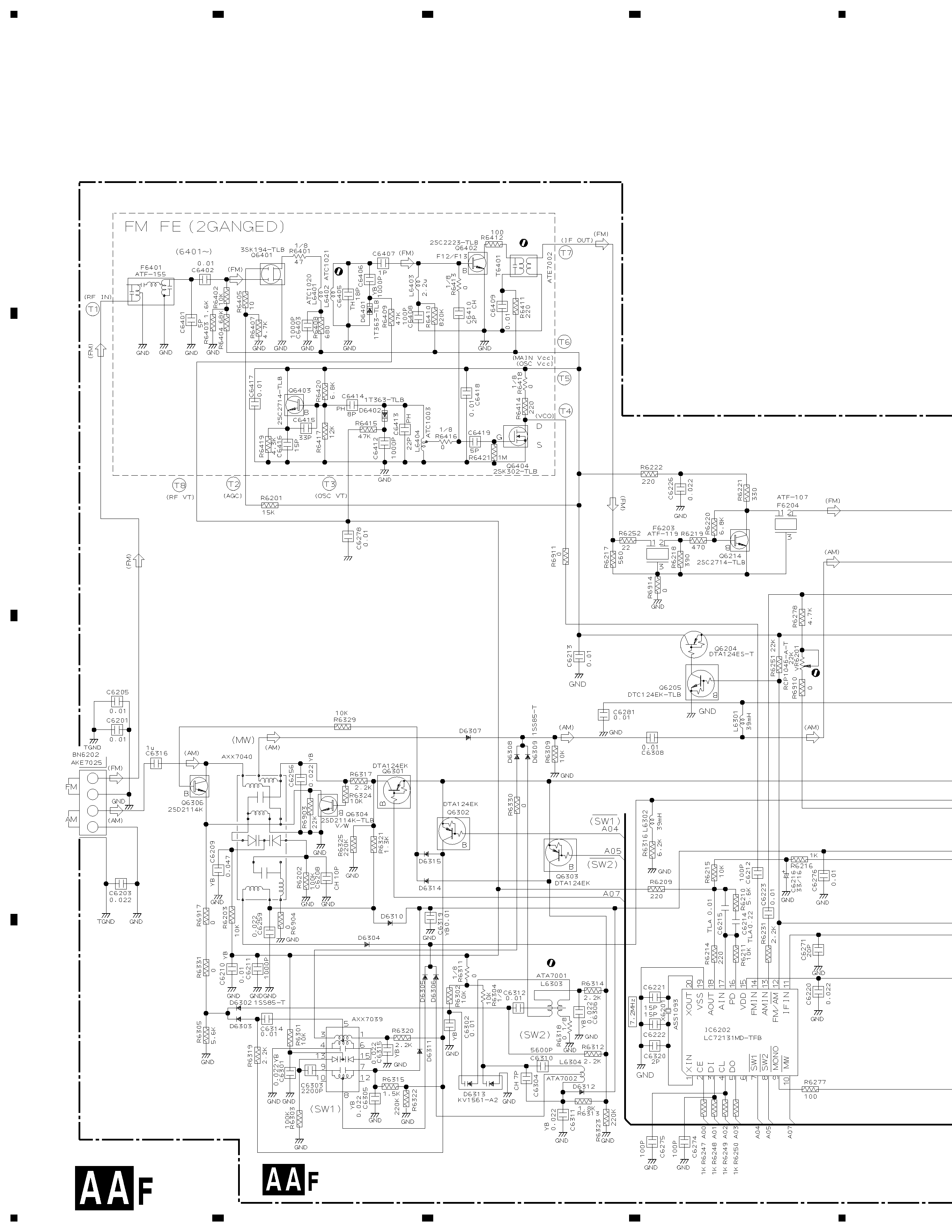
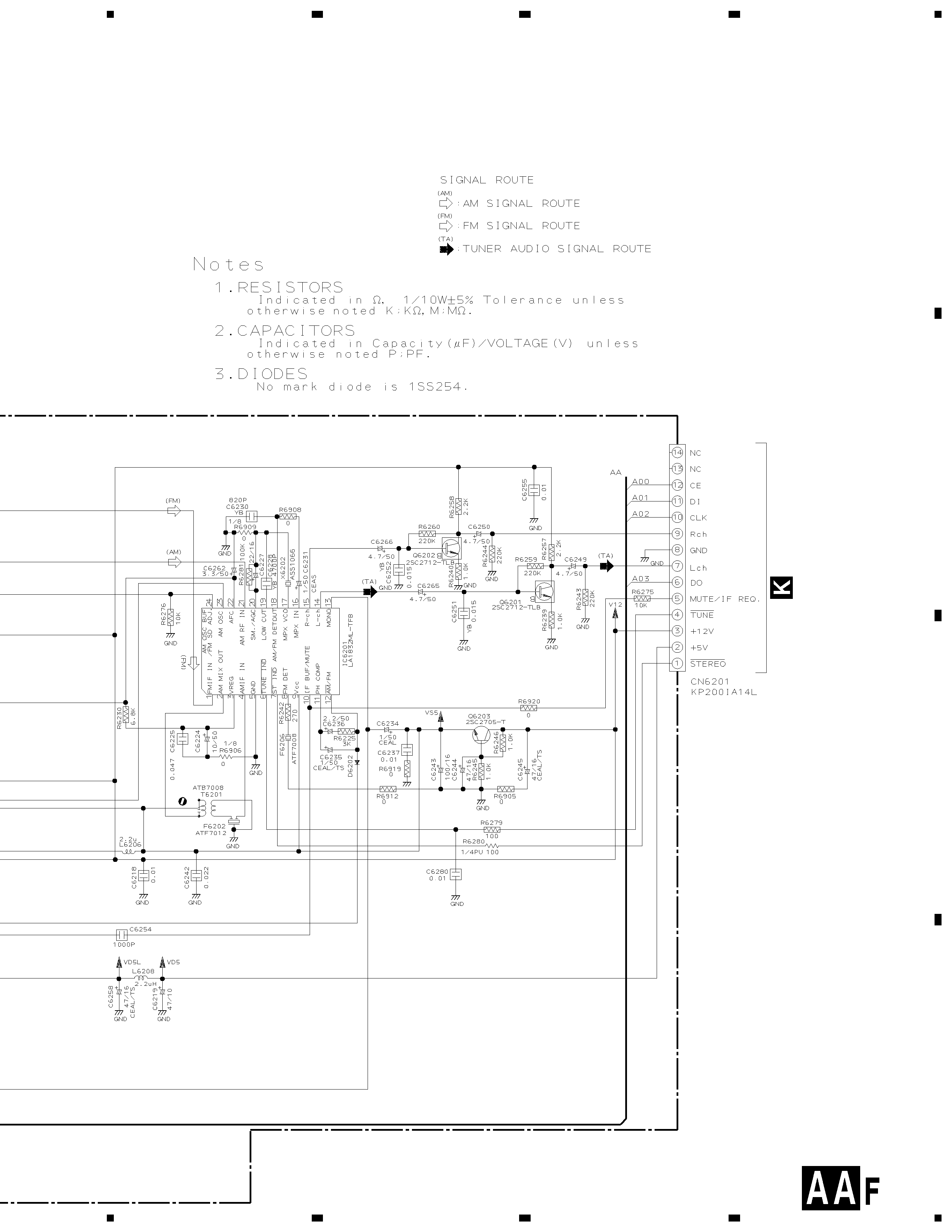
A
B
C
D
1
23
4
12
3
4
FM/AM TUNER MODULE
(AXQ7062)
RF AMP
MIX AMP
BUFFER
IF AMP
PLL
FM +B SW
SW DRIVE
AM RF TUNING BLOCK
OSC
2. SCHEMATIC DIAGRAM
Note : When ordering service parts, be sure to refer to "EXPLODED VIEWS and PARTS LIST" or "PCB PARTS LIST"
2.1 FM/AM TUNER MODULE (AXQ7062)
XR-A660SW, XR-A660EE
5
A
B
C
D
5
67
8
5
6
7
8
CN1054
AF AMP
REGULATOR
AF AMP