ORDER NO.
PIONEER ELECTRONIC CORPORATION 4-1, Meguro 1-Chome, Meguro-ku, Tokyo 153-8654, Japan
PIONEER ELECTRONICS SERVICE, INC. P.O. Box 1760, Long Beach, CA 90801-1760, U.S.A.
PIONEER ELECTRONIC (EUROPE) N.V. Haven 1087, Keetberglaan 1, 9120 Melsele, Belgium
PIONEER ELECTRONICS ASIACENTRE PTE. LTD. 253 Alexandra Road, #04-01, Singapore 159936
PIONEER ELECTRONIC CORPORATION 1999
KUXQ/CA
O
AC120V
FILE-TYPE COMPACT DISC PLAYER
RRV2112
TZZR MAR. 1999 Printed in Japan
PD-F17
¶ Refer to the service manual RRV2085 for PD-F958/KUXQ/CA.
Remarks
Type
Model
PD-F17
Power Requirement
THIS MANUAL IS APPLICABLE TO THE FOLLOWING MODEL(S) AND TYPE(S).
1. CONTRAST OF MISCELLANEOUS PARTS ..... 2
2. SCHEMATIC DIAGRAM .................................... 8
3. PCB CONNECTION DIAGRAM ......................... 9
CONTENTS
PD-F17
2
1. CONTRAST OF MISCELLANEOUS PARTS
NOTES :
÷ Parts marked by " NSP " are generally unavailable because they are not in our Master Spare Parts List.
÷ The
mark found on some component parts indicates the importance of the safety factor of the part.
Therefore, when replacing, be sure to use parts of identical designation.
÷ Reference Nos. indicate the pages and Nos. in the service manual for the base model.
÷ When ordering resistors, first convert resistance values into code form as shown in the following examples.
Ex. 1
When there are 2 effective digits (any digit apart from 0), such as 560 ohm and 47k ohm (tolerance is shown by
J = 5%, and K = 10%).
560
= 56 × 101= 561 ................................................... RD1/4PU 5 6 1 J
47k
= 47 × 10 3 = 473 .................................................. RD1/4PU 4 7 3 J
0.5
= R50 ...................................................................... RN2H Â 5 0 K
1
= 1R0 ......................................................................... RS1P 1 Â 0 K
Ex. 2
When there are 3 effective digits (such as in high precision metal film resistors).
5.62k
= 562 × 10 1 = 5621 ........................................... RN1/4PC 5 6 2 1 F
7 CONTRAST TABLE
PD-F17/ KUXQ/CA and PD-F958/KUXQ/CA are constructed the same except for the following:
Note :
÷ The numbers in the remarks column correspond to the numbers on the exploded diagram, Refer to "EXPLODED VIEWS".
EXTERIOR
NSP
MOTHER BOARD ASSY
PWM2269
PWM2272
P6-1
MAIN BOARD ASSY
PWZ3895
PWZ3898
P6-2
POWER BOARD ASSY
PWZ3900
PWZ3902
P6-3
DISPLAY BOARD ASSY
PWZ3904
PWZ3905
P6-4
NSP
SWITCH BOARD ASSY
PWZ3907
PWZ3908
NSP
HEADPHONE BOARD ASSY
Not used
PWZ3911
No.1
NSP
COAXIAL OUTPUT BOARD ASSY
Not used
PWZ3917
No.2
P6-14
Foot Assy
REC1263
Not used
P6-18
Rear Base
PNA2452
PNA2502
P6-20
Insulator
PNW2766
PNW2766
(X2)
(X4)
P6-46
Name Plate
PAM1776
PAN1376
P6-50
Operation Panel
PNW2869
PNW2918
P6-52
Hood
PNW2865
PNW2919
Headphone Knob
Not used
PAC1707
No.3
LED Lens
Not used
PNW2019
No.4
SR Angle
Not used
PNB1192
No.5
PACKING
P3-5
NSP
Warranty Card
ARY7023
ARY7007
P3-7
Operating Instructions (English)
PRB1278
PRB1289
P3-11
Packing Case
PHG2337
PHG2374
Ref.
No.
Remarks
PD-F958/
PD-F17/
KUXQ/CA
KUXQ/CA
Part No.
Mark
Symbol and Description
PD-F17
3
EXPLODED VIEWS
EXTERIOR SECTION
Rear Base
Under Base
Screw (IBZ30P080FZK)
Screw
(IBZ30P060FMC)
No.4
Operation Panel
lnsulator
No.3
No.1
Name Plate
No.5
No.2
Screw
(IBZ30P060FMC)
Screw
(BBZ30P080FZK)
PD-F17
4
C81, C332, C333, C367, C461
Not used
CKCYF103Z50
C475, C477, C4276, C4287
Not used
CKCYF103Z50
C185, C323
CKCYF103Z50
Not used
C321
CFTLA104J50
Not used
C322
CEAT101M10
Not used
C331
Not used
CEAT470M16
C341, C342
CCCCH120J50
Not used
C365, C395, C413 C416, C4277
Not used
CFTLA104J50
C388, C389
Not used
CCCSL101J50
C401
Not used
CEAT471M6R3
C403
Not used
CCCCH120J50
C404
Not used
CCCCH220J50
C429, C430, C435 C438
Not used
CCCSL390J50
C431, C432
Not used
CEAT330M16
C481, C482
CCCSL390J50
Not used
CN401, CN951
Not used
52147-0310
D451, D452
Not used
1SS254
IC341
Not used
PD0236AM
IC401
Not used
PD2029A
IC406
Not used
BA15218
JA321
GP1F32T
Not used
L151, L152, L307, L309, L351
Not used
RTF1167
Q451, Q452
Not used
DTC124ES
Q453, Q454
Not used
2SJ103
R310 R312, R411 R413
Not used
RD1/4PU241J
R341
RD1/4PU271J
Not used
R342
RD1/4PU105J
Not used
R364, R451, R452
Not used
RD1/4PU103J
R365
RD1/4PU103J
Not used
R375
RD1/4PU471J
RD1/4PU241J
R401, R457, R458, R472, R473
Not used
RD1/4PU102J
R405 R410
Not used
RD1/4PU471J
R427 R430
Not used
RD1/4PU223J
R435, R436
Not used
RD1/4PU163J
R437, R438
RD1/4PU473J
RD1/4PU163J
R439 R442
RD1/4PU823J
RD1/4PU443J
R470, R471
Not used
RD1/4PU470J
R481, R482, R485, R486
RD1/4PU223J
Not used
R487 R490
RD1/4PU104J
Not used
X341
PSS1008
Not used
X401
Not used
PSS1008
Note : Refer to "2.SCHEMATIC DIAGRAM".
MAIN BOARD ASSY
PWZ3898 and PWZ3895 are constructed the same except for the following:
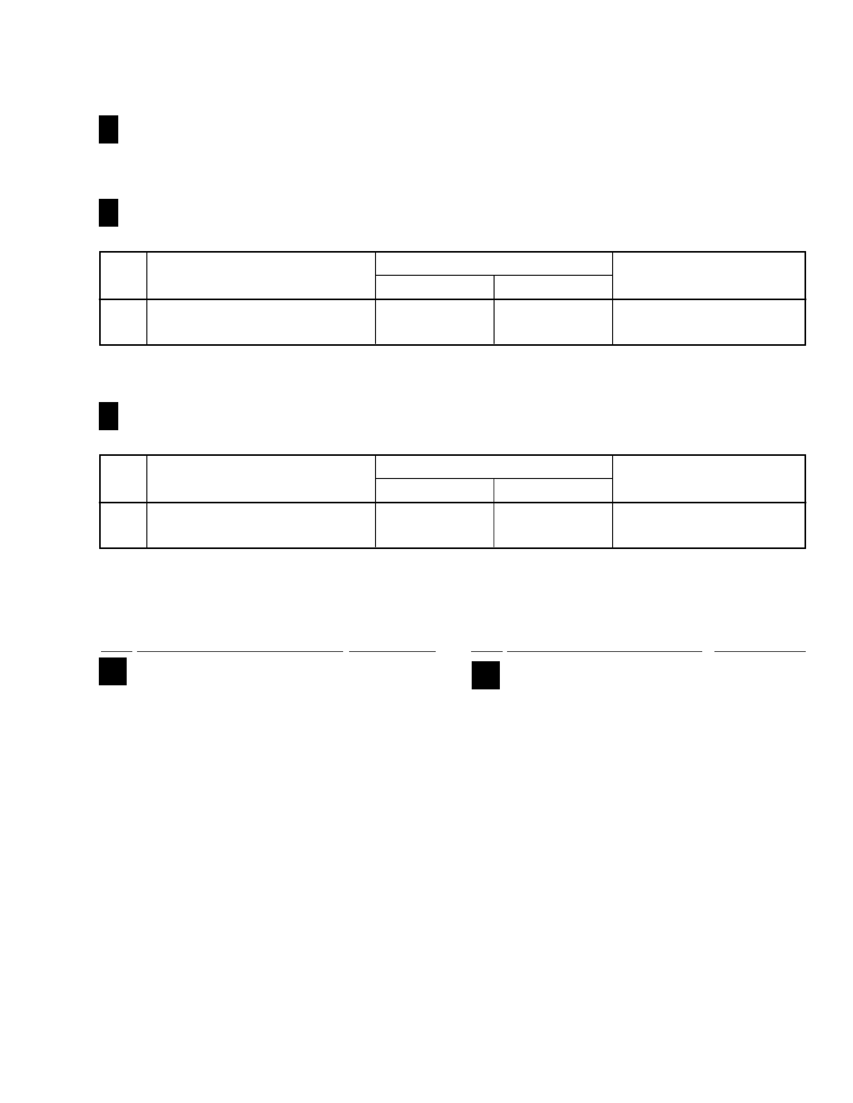
CONTRAST OF PCB ASSEMBLIES
Mark
Symbol and Description
Part No.
PWZ3895
PWZ3898
Remarks
H F
PD-F17
5
COAXIAL OUTPUT BOARD ASSY
(PWZ3917)
SEMICONDUCTORS
IC951
(LOGIC)
TA74HCU04AP
COIL
L952
(COIL)
PTL1003
CAPACITORS
C959
CCCSL101J50
C954
CEAT101M10
C951
CEAT470M16
C955, C957, C958, C961
CFTLA104J50
C952
CKCYF103Z50
RESISTORS
R951, R953
RD1/4PU471J
R952
RD1/4PU750J
OTHERS
JA951
OPTICAL LINK OUT
GP1F32T
JA952
1P JACK
RKB1012
3P Cable Holder
51048-0300
J951
2mm JUMPER WIRE
D20PDY0350G
Mark No.
Description
Part No.
HADPHONE BOARD ASSY (PWZ3911)
COILS AND FILTERS
L501, L504, L505 (AXIAL INDUCTOR)
LAU1R0J
CAPACITORS
C503
CKCYF473Z50
RESISTORS
VR501 (0.5k
)
PCS1003
OTHERS
JA501
HADPHONE JACK
RKN1002
3P Cable Holder
51048-0300
J501
2mm JUMPER WIRE
D20PDY0315E
C714
Not used
CKCYF103Z50
NSP
J703
Not used
DE010WE0
Mark
Symbol and Description
Part No.
PWZ3904
PWZ3905
Remarks
DISPLAY BOARD ASSY
PWZ3905 and PWZ3904 are constructed the same except for the following:
Note : Refer to "2.SCHEMATIC DIAGRAM".
D751
Not used
PCX1019
R751
Not used
RD1/4PU471J
Mark
Symbol and Description
Part No.
PWZ3907
PWZ3908
Remarks
SWITCH BOARD ASSY
PWZ3908 and PWZ3907 are constructed the same except for the following:
Note : Refer to "2.SCHEMATIC DIAGRAM".
POWER BOARD ASSY
Although PWZ3900 and PWZ3902 are different in part number, they consist of the same components.
Q
¶ PCB PARTS LIST
P
Mark No.
Description
Part No.
I F
M F
L F