Model
Service Manual
CD Mechanism Module
DEH-P630/X1N/UC
CRT2648
CXK5500
DEH-P7300R/X1N/EW
CRT2649
DEH-P730/X1N/UC
CRT2650
DEH-P7350/X1N/ES
CRT2651
PIONEER CORPORATION
4-1, Meguro 1-Chome, Meguro-ku, Tokyo 153-8654, Japan
PIONEER ELECTRONICS SERVICE INC.
P.O.Box 1760, Long Beach, CA 90801-1760 U.S.A.
PIONEER EUROPE NV
Haven 1087 Keetberglaan 1, 9120 Melsele, Belgium
PIONEER ELECTRONICS ASIACENTRE PTE.LTD. 253 Alexandra Road, #04-01, Singapore 159936
C PIONEER CORPORATION 2001
K-ZZA. MAR. 2001 Printed in Japan
ORDER NO.
CRT2624
CD MECHANISM MODULE
CX-977
Service
Manual
- This service manual describes the operation of the CD mechanism module incorporated in models
listed in the table below.
- When performing repairs use this manual together with the specific manual for model under repair.
CONTENTS
1. CIRCUIT DESCRIPTIONS ...........................................2
2. MECHANISM DESCRIPTIONS.................................26
3. DISASSEMBLY .........................................................28
2
CX-977
1. CIRCUIT DESCRIPTIONS
From divisional viewpoint, the CX-977 is roughly divided into four sections, namely, Preamplifier, Servo, Power Supply
and Loading Control.
This LSI realizes eight types of automatic adjustments (controls) through cooperative work between Preamplifier and
Servo unit.
Because the system uses the single power source (+ 5v) specification, reference voltages used in the servo system
(Preamplifier, Servo DSP and Pickup) are all Vref (2.1V).
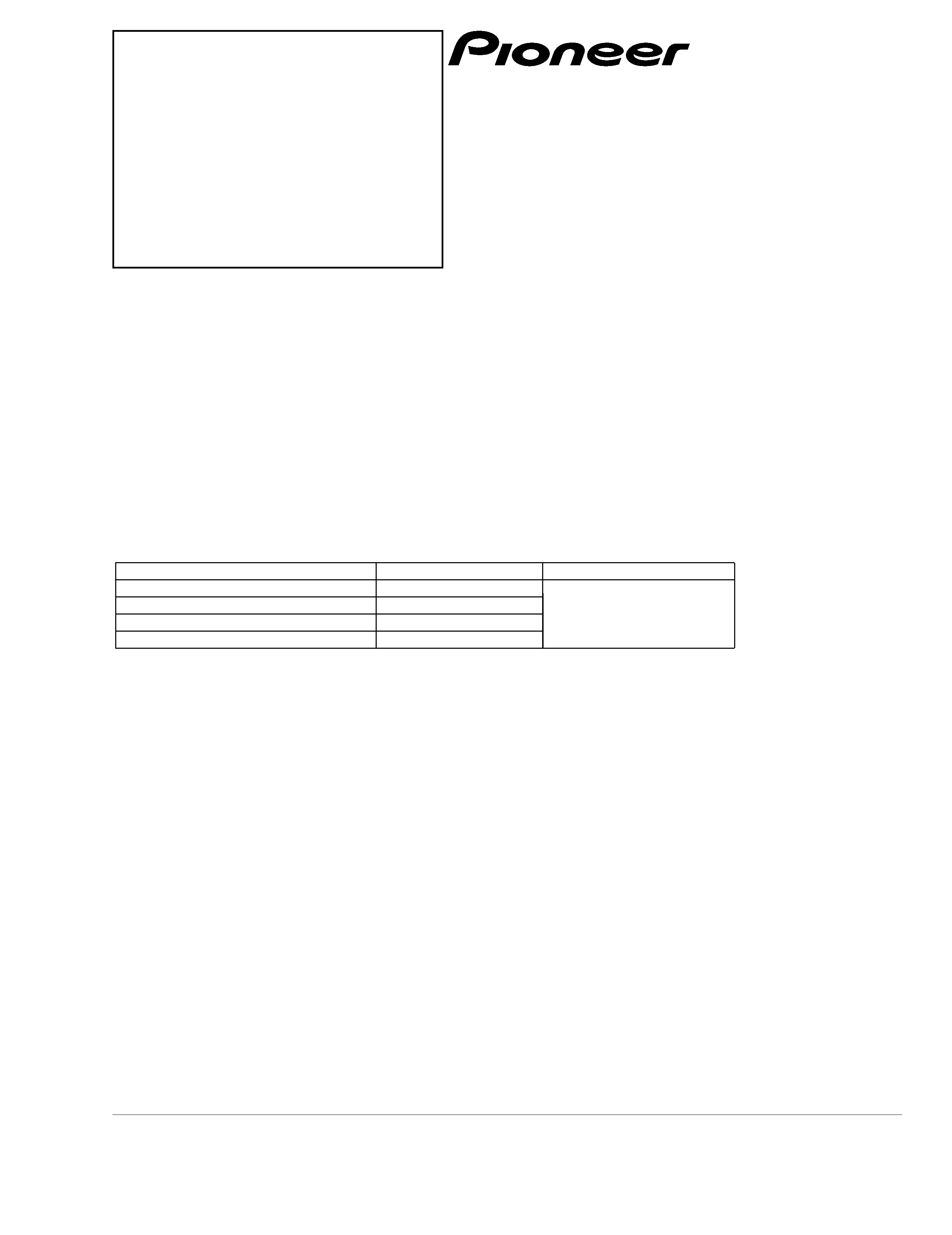
1.1 PREAMPLIFIER (TA2153FN; IC101)
The Preamplifier processes output signals sent from the Pickup and generates signals to supply to each unit of the
next stage, that is, Servo, Demodulator or Control. It also performs power control of Pickup's laser diode. Signals from
the Pickup are I-V-converted by the Preamplifier, which is built-in in Pickup's photo detector, and then added-up by the
RF amplifier to obtain signals such as RF, FE and TE.
Reference voltage, Vref (2.1v), is output from #19 pin of the IC, and 2Vref (4.2v) is supplied to the Servo DSP as the
reference voltage to determine its D range of A/D input.
Fig. 1: TA2153FN circuit
3
CX-977
1) Focus Error Amplifier unit
In this sub-unit, outputs from the photo detector, namely, (A+C) and (B+D), are processed in the differential amplifier
and further in the error amplifier, and then, (A+C-B-D) is output as FE signal from #16 pin of IC101 (TA2153FN).
Low frequency component of voltage FE is expressed as:
FE = (A+C-B-D) x (150k/(51k+1k)) x (60k/60k) x (120k/60k) = 5.77 times
In FE output, "S" curve of approximately 1.45 Vpp on the basis of Vref is obtained. The cutoff frequency of the
succeeding amplifier is 11.4 kHz.
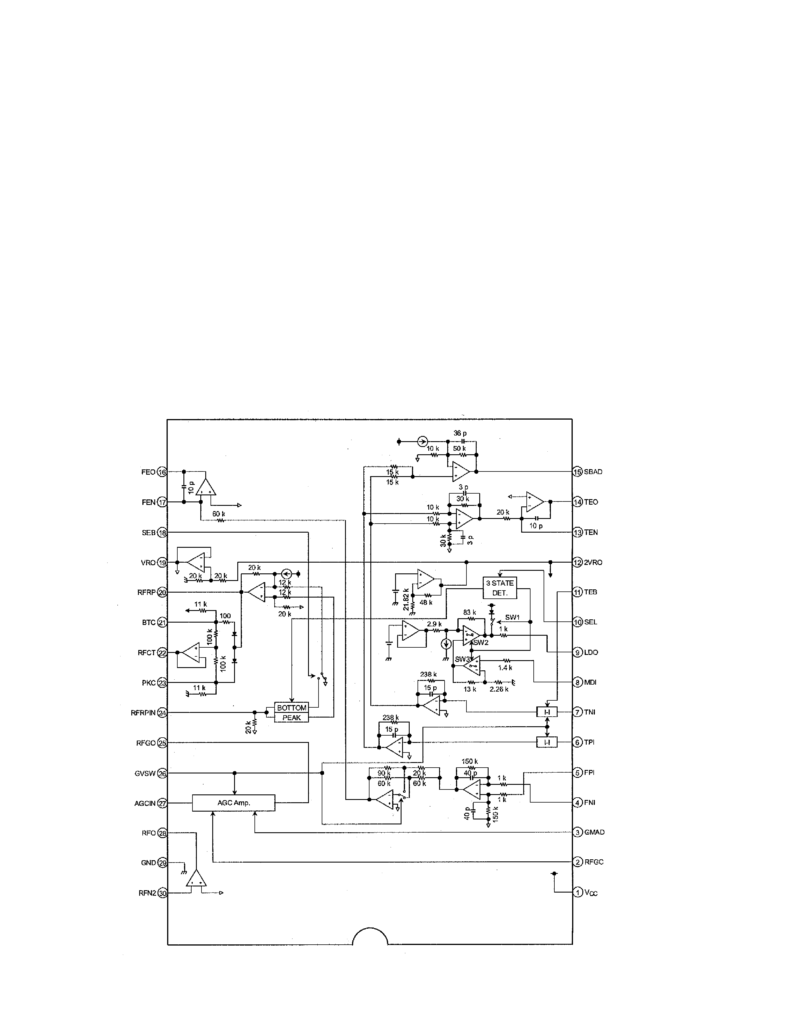
2) Tracking Error Amplifier unit
In this sub-unit, outputs from the photo detector, namely, E and F, are processed in the differential amplifier and
further in the error amplifier, and then, (E-F) is output as TE signal from #14 pin of IC101 (TA2153FN).
Low frequency component of voltage TE is expressed as:
TE = (E-F) x 300k/100k x 82k/20k = 5.8 times
In TE output, "TE" waveform of approximately 1.51 Vpp on the basis of Vref is obtained. The cutoff frequency of the
succeeding amplifier is 20 kHz.
Fig. 2: FE circuit
Fig. 3: TE circuit
4
CX-977
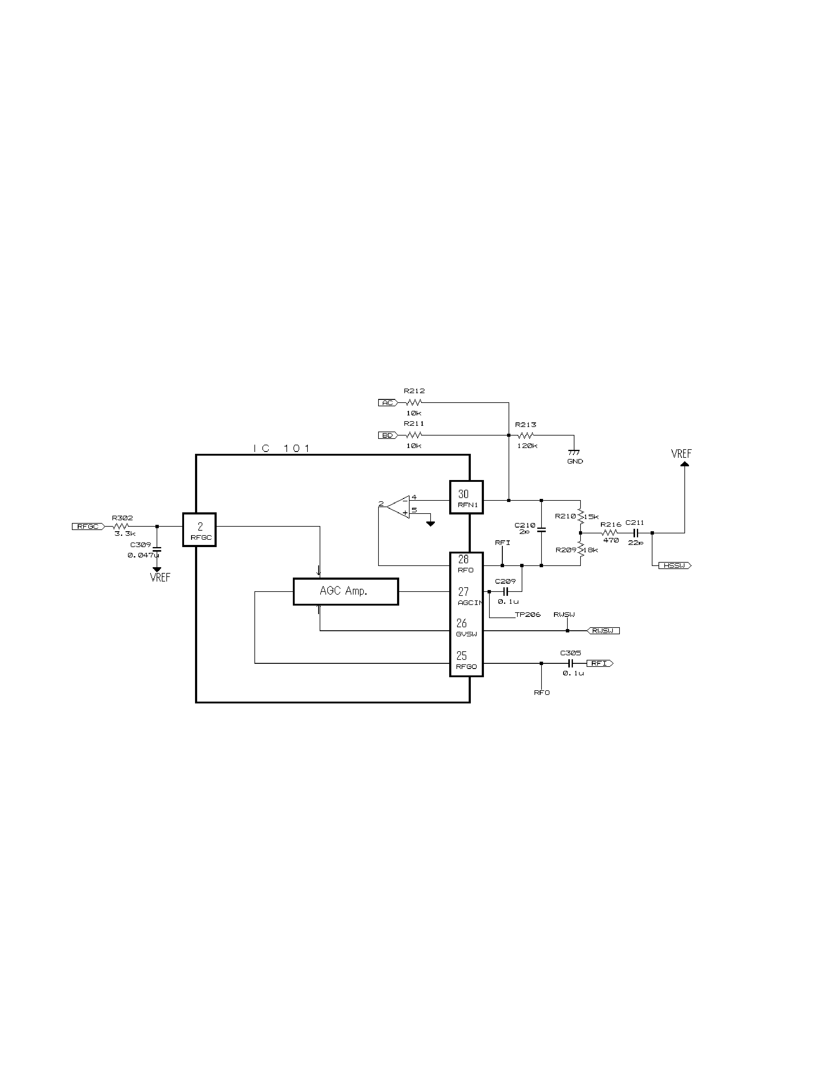
3) RF Amplifier unit
Outputs from the photo detector, namely, (A+C) and (B+D), are added up, amplified and equalized in the Head
Amplifier LSI (TA2153FN). The processed-signals are output to RFI terminal as RF signals (These signals are used to
check eye patterns).
Low frequency component of voltage RFI is expressed as:
RFI = (A+B+C+D) x 5.43
RFI is used for RF Offset Control circuit. These RFI signals so output from #28 pin are AC-coupled outside the unit, and
then re-input to #27 pin and amplified by the RFAGC amplifier to obtain RFO signals.
TA2153FN has built-in function for RFAGC adjustment, as described later, and through such function, the gain of
RFAGC is controlled so that RFO output stays within 1.2 ± 0.3 Vpp range.
Also, RFO signals are used for EFM and RFAGC Adjustment circuit. They are further used to generate RFRP and RFCT
signals, both of which are used for track counting.
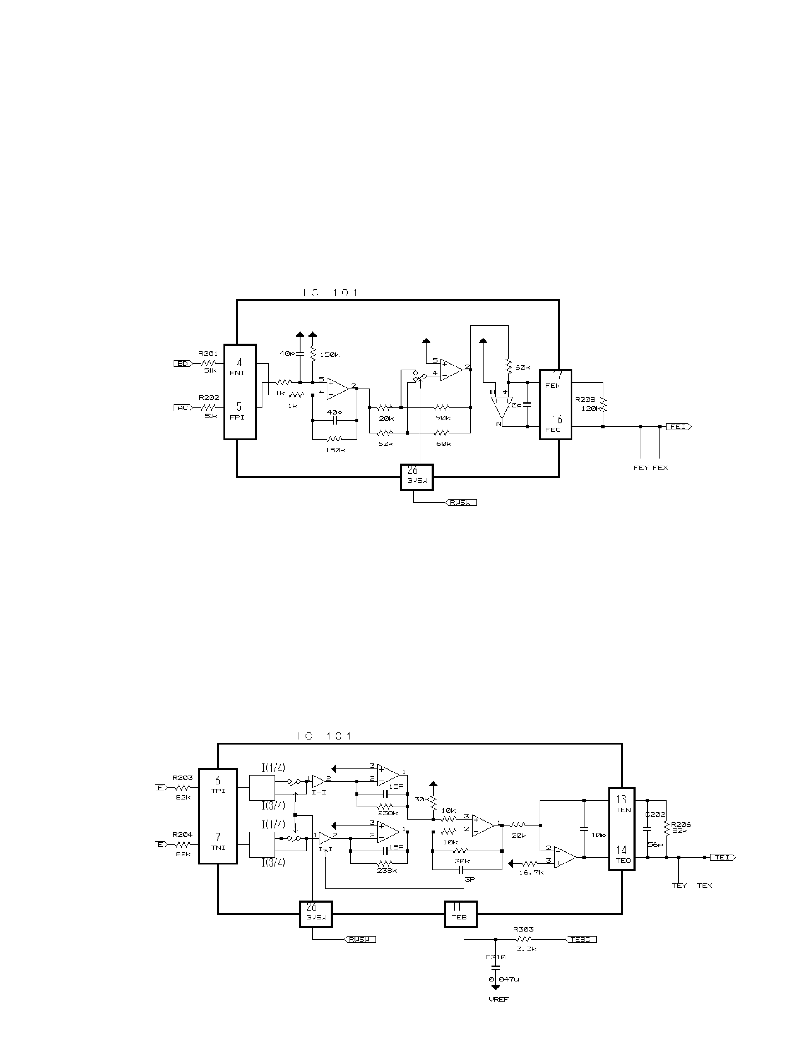
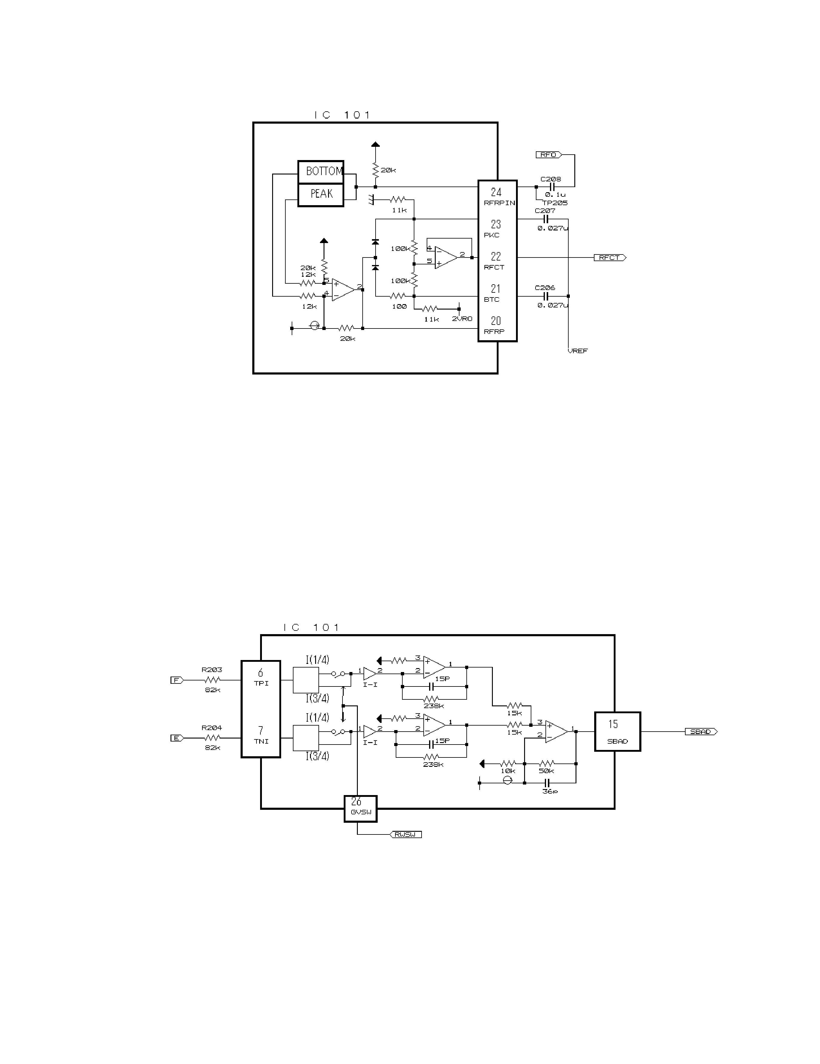
4) RFRP and RFCT Signal Circuit unit
RFCT signals are generated through the Head Amplifier (IC101). A RFCT signal is the difference signal that represents
the difference between the peak and bottom level of RF signal. RFRP and RFCT can be monitored at TP203 (#20 pin of
IC101, namely, TA2153FN) and TP204 (#20 pin of IC101) respectively.
Size-comparison among TE, RFRP and RFCT signals is performed by the Hysteresis Comparator in IC201 (TC9495F2),
and through such comparison, track information (TEZC and RFZC signal) is generated. Based on these signals,
information to determine tracking speed of the lens when it moves on the disk is generated. Also based on these
signals, number of tracks is counted.
Fig. 4: RF circuit
5
CX-977
5) SBAD Signal Circuit unit
In this unit, outputs from the photo detector, namely, E and F are processed through the addition amplifier. That is, E
and F are added together and (E+F) signal is output from #15 pin of IC101 (TA2153FN), as SBAD signal.
This SBAD signal, along with Focus Error signal, is used as one of the conditions that the system uses to internally
judge Focus ON/OFF based on them.
Also, SBAD signal is used to detect defects: defects that may be detected when the Pickup passes a scratch on the
disk, for instance.
Fig. 5: RFRP and RFCT circuit
Fig. 6: SBAD circuit