SERVICE MANUAL
DIGITAL VIDEO CAMERA RECORDER
LEVEL
2
· For ADJUSTMENTS (SECTION 6), refer to SERVICE MANUAL, ADJ (9-876-865-51).
· For INSTRUCTION MANUAL, refer to SERVICE MANUAL, LEVEL 1 (9-876-865-41).
· Reference number search on printed wiring boards is available.
· TO TAKE OUT A DISC WHEN DISC COVER DOES NOT OPEN (FORCE OPEN)
Link
SERVICE NOTE
DISASSEMBLY
BLOCK DIAGRAMS
SCHEMATIC DIAGRAMS
PRINTED WIRING BOARDS
REPAIR PARTS LIST
SPECIFICATIONS
SERVICE NOTE
DISASSEMBLY
BLOCK DIAGRAMS
SCHEMATIC DIAGRAMS
PRINTED WIRING BOARDS
REPAIR PARTS LIST
SPECIFICATIONS
Link
Revision History
Revision History
Ver 1.1 2005. 05
On the CD-563, VF-166, MD-114, MD-120 and VC-395 board
This service manual provides the information that is premised the circuit board replacement service and not intended repair
inside the CD-563, VF-166, MD-114, MD-120 and VC-395 board.
Therefore, schematic diagram, printed wiring board, waveforms, mounted parts location and electrical parts list of the CD-563,
VF-166, MD-114, MD-120 and VC-395 board are not shown.
The following pages are not shown.
Mounted parts location ....................... Pages 4-94 to 4-97
Electrical parts list .............................. Pages 5-15 to 5-27
How to use
Acrobat Reader
How to use
Acrobat Reader
Schematic diagram ............................. Pages 4-17 to 4-60
Printed wiring board ............................ Pages 4-73 to 4-90
Waveforms ........................................... Page 4-92
Sony EMCS Co.
2005E1600-1
©2005.05
Published by DI Technical Support Section
9-876-865-31
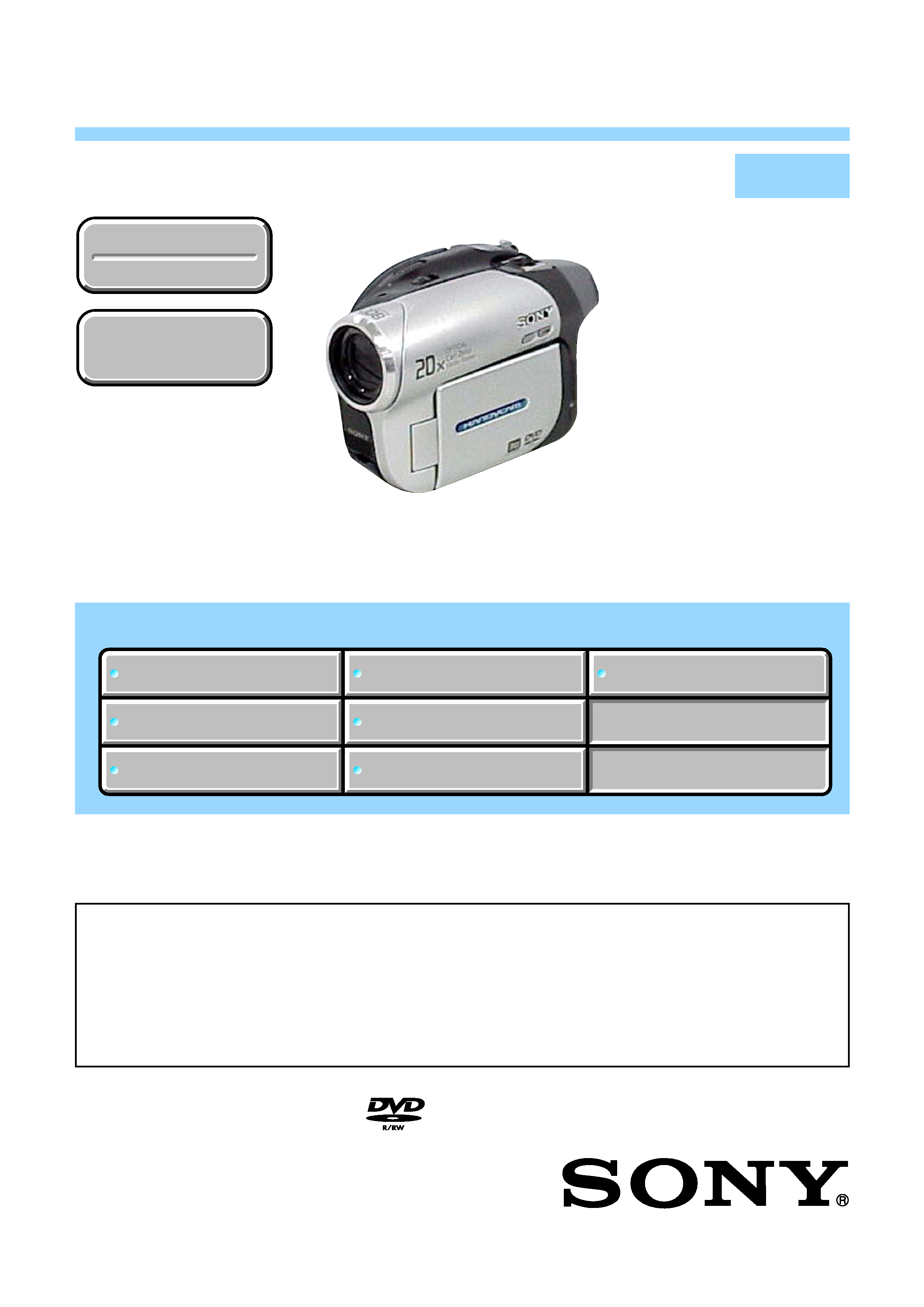
DCR-DVD92/DVD92E/DVD103/DVD602/
DVD602E/DVD653/DVD653E
RMT-835
DCR-DVD92/DVD92E/DVD103/DVD602/DVD602E/DVD653/DVD653E
DCR-DVD92/DVD103
US Model
Canadian Model
DCR-DVD92E
AEP Model
UK Model
North European Model
DCR-DVD602E/
DVD653E
Australian Model
DCR-DVD602
Korea Model
DCR-DVD92/DVD103/
DVD602/DVD602E/
DVD653/DVD653E
E Model
DCR-DVD653/DVD653E
Tourist Model
DCR-DVD92
Brazilian Model
DCR-DVD103
Argentina Model
DCR-DVD653E
Hong Kong Model
Photo : DCR-DVD92E

-- 2 --
DCR-DVD92/DVD92E/DVD103/DVD602/DVD602E/DVD653/DVD653E
SPECIFICATIONS
Color temperature [AUTO], [ONE PUSH],
[INDOOR] (3 200 K),
[OUTDOOR] (5 800 K)
Minimum
illumination
11 1x (lux) (F1.8)
0 lx (lux) (in the NightShot
plus function)
*3
*1 "Exif" is a file format for still images,
established by the JEITA (Japan Electronics
and Information Technology Industries
Association). Files in this format can have
additional information such as your camcorder's
setting information at the time of recording.
*2 In 16:9 mode, the focal length figures are actual
figures resulting from wide angle pixel readout.
*3 Objects unable to be seen due to the dark can be
shot with infrared lighting.
·
Manufactured under license from Dolby
Laboratories.
Input/Output connectors
DCR-DVD92/DVD602/DVD92E/DVD602E
Audio/Video
10 pin connector
output
Video signal: 1 Vp-p, 75
(ohms), unbalanced
Luminance signal: 1 Vp-p, 75
(ohms), unbalanced
Chrominance signal:
0.286 Vp-p, 75
(ohoms),
unbalanced (DVD92/DVD602)
0.3 Vp-p, 75
(ohoms),
unbalanced (DVD92E/DVD602E)
Audio signal: 327 mV (at Load
impedance 47 k
(kilohms)),
Output impedance less than 2.2
k
(kilohms)
REMOTE jack
Stereo mini-minijack (Ø 2.5
mm)
DCR-DVD103/DVD653/DVD653E
Audio/Video
10 pin connector
input/output
Input/Output auto switch
Video signal: 1 Vp-p, 75
(ohms), unbalanced
Luminance signal: 1 Vp-p, 75
(ohms), unbalanced
Chrominance signal:
Audio signal: 327 mV (at Load
impedance 47 k
(kilohms)),
Input inpedance more than
47 k
(kilohms), Output
impedance less than 2.2 k
(kilohms)
USB jack
mini-B
REMOTE jack
Stereo mini-minijack (Ø 2.5
mm)
LCD screen
Picture
6.2 cm (2.5 type)
Total number
123 200 (560
×220)
of pixels
General
Power
7.2 V (battery pack)
requirements
8.4 V (AC adaptor)
Average power
During camera recording using
consumption
LCD
(when using the DCR-DVD92/DVD602/DVD92E/
DVD602E:3.4W
battery pack)
DCR-DVD103/DVD653/
DVD653E: 3.4W
Viewfinder
DCR-DVD92/DVD602/DVD92E/
DVD602E: 3.0W
DCR-DVD103/DVD653/
DVD653E: 3.0W
Operating
0
°C to + 40°C (32°F to 104°F)
temperature
Storage
-20
°C to + 60°C (-4°F to
temperature
+ 140
°F)
Dimensions
(Approx.)
57
× 87 × 131mm (2 1/4 × 3
1/2
× 5 1/4 in.) (w×h×d)
Mass (Approx.)
440 g (15 oz) main unit only
500 g (1 lb 1 oz) including the
NP-FP50 rechargeable battery
pack and disc
Supplied
See page 5-12.
accessories
AC Adaptor AC-L25A/L25B
Power
AC 100 - 240 V, 50/60 Hz
requirements
Current
0.35 - 0.18 A
consumption
Power
18W
consumption
Output voltage
DC 8.4V*
Operating
0
°C to + 40°C (32°F to 104°F)
temperature
Storage
-20
°C to + 60°C (-4°F to
temperature
+ 140
°F)
Dimensions
56 31 100 mm (2 1/4
×
(Approx.)
1 1/4
× 4 in.) (w×h×d)
excluding the projecting parts
Mass (Approx.)
190 g (6.7 oz) excluding the
power cord
* See at the label of AC adaptor for other
specifications.
Rechargeable battery pack
Maximum
DC 8.4V
output voltage
Output voltage
DC 7.2V
Capacity
4.9 wh (680 mAh)
Dimensions
31.8 18.5 45.0 mm
(Approx.)
(1 5/16
× 3/4 × 1 13/16 in.)
(w
×h×d)
Mass (Approx.)
40 g (1.5 oz)
Operating
0
°C to + 40°C (32°F to 104°F)
temperature
Type
Li-ion
Design and specifications are subject to change
without notice.
System
Video
MPEG2/JPEG (Still images)
compression
format
Audio compression DCR-DVD92/DVD602/DVD92E/
DVD602E
format
Dolby Digital 2ch
Dolby Digital Stereo Creator
DCR-DVD103/DVD653/DVD653E
Dolby Digital 2/5.1ch
Dolby Digital 5.1 Creator
Video signal
NTSC color, EIA standards
(DVD92/DVD103/DVD602/DVD653)
PAL color, EIA standards
(DVD92E/DVD602E/DVD653E)
Usable discs
8cm DVD-R/
DVD-RW/
DVD+RW
Recording
Movie
format
DVD-R:DVD-VIDEO
DVD-RW:DVD-VIDEO
(VIDEO mode), DVD-
VideoRecording (VR mode)
DVD+RW:DVD+RW Video
Still image
Exif *1 Ver.2.2
Recording/
HQ: Approx. 20 min
playback time
SP: Approx. 30 min
LP: Approx. 60 min
Viewfinder
Electric viewfinder
DCR-DVD92/DVD602/DVD92E/
DVD602E:
monochrome
DCR-DVD103/DVD653/DVD653E:
color
Image device
3 mm (1/6 type) CCD (Charge
Coupled Device)
Gross: Approx. 680 000 pixels
Effective (Movie) :
Approx. 340 000 pixels
Effective (Still) :
Approx. 340 000 pixels
Lens
Carl Zeiss Vario-Tessar
Filter diameter:30mm (1 3/16
in.)
Optical:20, Digital:40, 800
F=1.8-3.1
Focal length
f=2.3 - 46 mm (3/32 - 1 13/16
in.)
When converted to a 35 mm
still camera
For movies:
44 - 880mm (1 3/4 - 34 3/4 in.)
For still images:
44 - 880mm (1 3/4 - 34 3/4 in.)
0.286 Vp-p, 75
(ohoms),
unbalanced (DVD103/DVD653)
0.3 Vp-p, 75
(ohoms),
unbalanced (DVD653E)
· Abbreviation
CND : Canadian model
HK
: Hong Kong model
AUS : Australian model
NE
: North European model
KR
: Korea model
JE
: Tourist model
AR
: Argentina model
BR
: Brazilian model
DVD92E
AEP, NE, UK
PAL
DVD103
US, CND, E, AR
NTSC
a
Color
a
a
a
DVD92
US, CND, E, BR
NTSC
Destination
Color System
Remote
Commander
View Finder
USB Terminal
Line REC
Lens Barrier
DVD602
E, KR
NTSC
DVD653
E, JE
NTSC
Table for difference of function
DVD602E
E, AUS
PAL
DVD653E
E, HK, AUS, JE
PAL
W/B
W/B
a
Color
a
a
a
-- 3 --
DCR-DVD92/DVD92E/DVD103/DVD602/DVD602E/DVD653/DVD653E
1.
Check the area of your repair for unsoldered or poorly-soldered
connections. Check the entire board surface for solder splashes
and bridges.
2.
Check the interboard wiring to ensure that no wires are
"pinched" or contact high-wattage resistors.
3.
Look for unauthorized replacement parts, particularly
transistors, that were installed during a previous repair. Point
them out to the customer and recommend their replacement.
4.
Look for parts which, through functioning, show obvious signs
of deterioration. Point them out to the customer and
recommend their replacement.
5.
Check the B+ voltage to see it is at the values specified.
6.
Flexible Circuit Board Repairing
· Keep the temperature of the soldering iron around 270°C
during repairing.
· Do not touch the soldering iron on the same conductor of the
circuit board (within 3 times).
· Be careful not to apply force on the conductor when soldering
or unsoldering.
Unleaded solder
Boards requiring use of unleaded solder are printed with the lead-
free mark (LF) indicating the solder contains no lead.
(Caution: Some printed circuit boards may not come printed with
the lead free mark due to their particular size.)
: LEAD FREE MARK
Unleaded solder has the following characteristics.
· Unleaded solder melts at a temperature about 40
°C higher than
ordinary solder.
Ordinary soldering irons can be used but the iron tip has to be
applied to the solder joint for a slightly longer time.
Soldering irons using a temperature regulator should be set to
about 350
°C.
Caution: The printed pattern (copper foil) may peel away if the
heated tip is applied for too long, so be careful!
· Strong viscosity
Unleaded solder is more viscous (sticky, less prone to flow) than
ordinary solder so use caution not to let solder bridges occur such
as on IC pins, etc.
· Usable with ordinary solder
It is best to use only unleaded solder but unleaded solder may
also be added to ordinary solder.
SAFETY CHECK-OUT
SAFETY-RELATED COMPONENT WARNING!!
COMPONENTS IDENTIFIED BY MARK 0 OR DOTTED LINE WITH
MARK 0 ON THE SCHEMATIC DIAGRAMS AND IN THE PARTS
LIST ARE CRITICAL TO SAFE OPERATION. REPLACE THESE
COMPONENTS WITH SONY PARTS WHOSE PART NUMBERS
APPEAR AS SHOWN IN THIS MANUAL OR IN SUPPLEMENTS
PUBLISHED BY SONY.
ATTENTION AU COMPOSANT AYANT RAPPORT
À LA SÉCURITÉ!
LES COMPOSANTS IDENTIFÉS PAR UNE MARQUE 0 SUR LES
DIAGRAMMES SCHÉMATIQUES ET LA LISTE DES PIÈCES SONT
CRITIQUES POUR LA SÉCURITÉ DE FONCTIONNEMENT. NE
REMPLACER CES COMPOSANTS QUE PAR DES PIÈSES SONY
DONT LES NUMÉROS SONT DONNÉS DANS CE MANUEL OU
DANS LES SUPPÉMENTS PUBLIÉS PAR SONY.
CAUTION :
Danger of explosion if battery is incorrectly replaced.
Replace only with the same or equivalent type.
There are two types of the MD board of this model.
One is the MD-114 board and the other is the MD-120 board.
Method of identifying the two different MD boards is shown on page 4.
After correcting the original service problem, perform the following
safety checks before releasing the set to the customer.
CAUTION
Use of controls or adjustments or performance
procedures other than those specified herein may
result in hazardous radiation exposure.
WARNING!!
WHEN SERVICING, DO NOT APPROACH THE LASER
EXIT WITH THE EYE TOO CLOSELY. IN CASE IT IS
NECESSARY TO CONFIRM LASER BEAM EMISSION,
BE SURE TO OBSERVE FROM A DISTANCE OF MORE
THAN
30
cm
FROM THE
SURFACE
OF THE
OBJECTIVE LENS ON THE OPTICAL PICK-UP BLOCK.
CAUTION:
The use of optical instrument with this product will increase eye
hazard.
-- 4 --
DCR-DVD92/DVD92E/DVD103/DVD602/DVD602E/DVD653/DVD653E
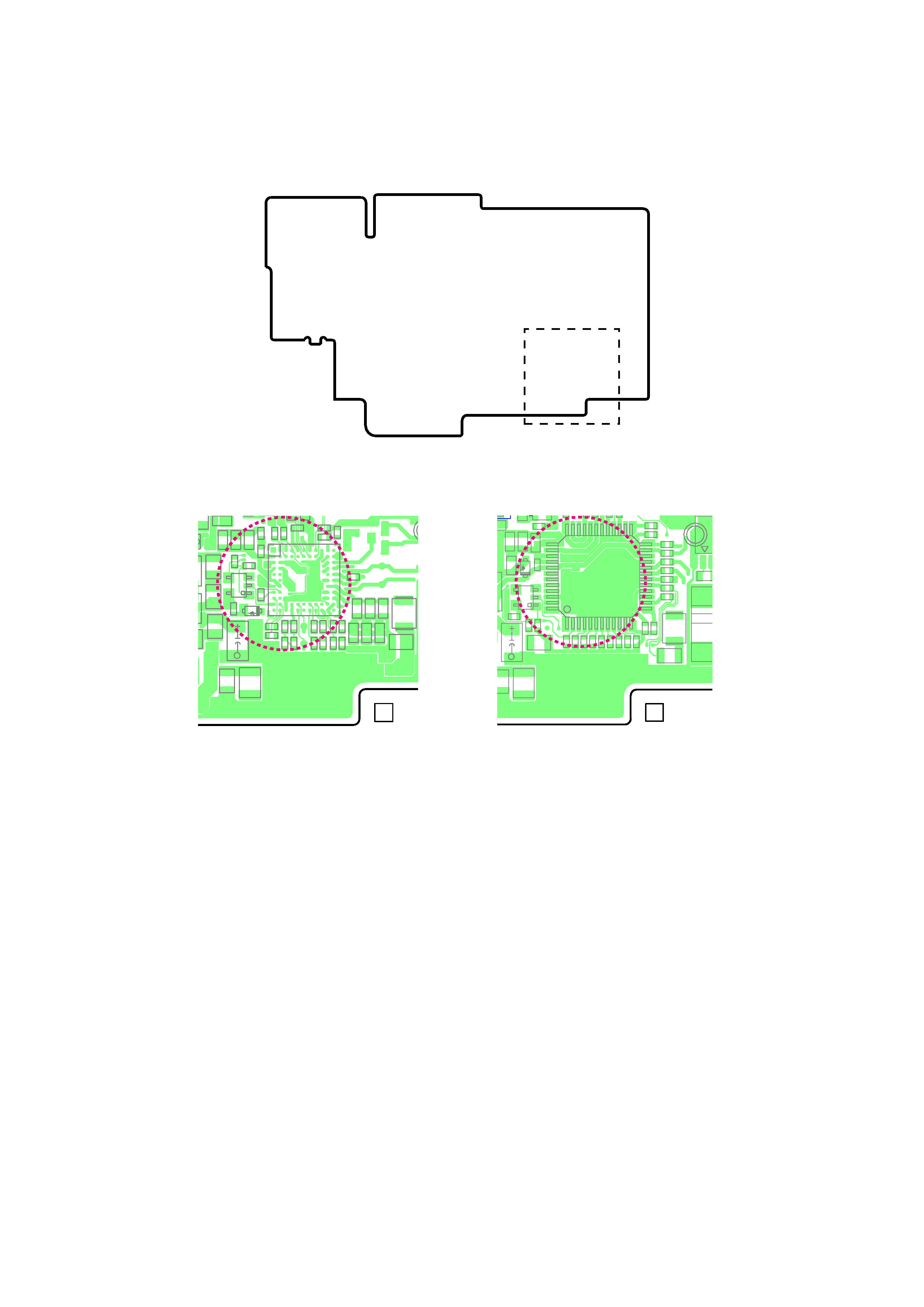
· How to identify the printed wiring boards (MD-114 BOARD/MD-120 BOARD)
MD-120 BOARD (SIDE B)
MD-114 BOARD (SIDE B)
11
1-863-772-
L4503
C4849
R
C4859
C4501
C4502
C4503
C4504
C
4
C
4
C4
5
C4508
C4509
C4510
C4511
C4512
C4513
C4514
C4515
C4516
C4517
C4518
FB4402
C4521
R4505
R4506
R4507
IC4501
IC4502
R4514
R4515
R4516
R4517
R4518
R4519
R4520
R4521
R4522
R4523
R4524
R4525
R4526
R4527
R4528
R4537
R4538
R4539
R4540
6
JL4511
JL4512
JL4514
JL4515
JL4516
JL4517
JL4513
JL4518
L4822
L482
L4812
1
54
3
A
P
E11
E10
F11
F10
G11
G10
H11
L8
K8
L7
K7
L6
K6
L5
K5
L4
K4
L3
K3
L2
K1
J1
J2
H1
H2
G1
G2
F1
H10
J11
J10
K11
K10
L9
K9
B1
A2
B10
L10
K2
B2
A3
B3
A4
B4
A5
B5
A6
B6
A7
B7
A8
B8
A9
B9
A10
B11
C11
C10
D11
D10
F2
E1
E2
D1
D2
C1
C2
A1
A11
L1
L11
2
1
2
1
2
1
1
1
2
1
2
1
2
1
2
1
1
5
4
3
12
12
12
12
12
12
12
12
2
1
2
1
2
1
2
1
2
1
2
1
2
1
2
1
2
1
12
2
1
1
12
1
1
1
1
1
1
1
1
12
1
12
11
1-866-564-
C460
IC
C4849
R
4
C4859
FB4401
4402
L4812
R4517
R4518
R4519
R4520
R4521
R4522
R4523
R4515
R4516
C4514
C4515
L4503
C4504
IC4502
C4512
C4510
C4511
R4506
R4508
R4509
R4510
R4512
R4514
C4513
C4503
C4505
R4505
IC4501
C4506
R4504
D4501
R4501
R4502
R4503
C
C
C
R
R4507
1
A
1
12
36
25
48
13
37
24
1
5
4
3
2
1
1
10
2
1
2
1
1
2
1
2
1
2
1
2
1
1
5
4
3
12
12
12
12
12
12
12
12
2
1
2
1
2
1
2
1
2
1
2
1
2
1
2
1
2
1
12
2
1
12
1
1
1
1
1
1
1
1
12
(MD-114)
(MD-120)

-- 5 --
DCR-DVD92/DVD92E/DVD103/DVD602/DVD602E/DVD653/DVD653E
TABLE OF CONTENTS
1.
SERVICE NOTE
1-1.
SERVICE NOTE ····························································· 1-1
1.
NOTE FOR REPAIR ······················································· 1-1
2.
POWER SUPPLY DURING REPAIRS ·························· 1-2
3.
TO TAKE OUT A DISC WHEN DISC COVER DOES
NOT OPEN (FORCE OPEN) ········································· 1-2
4.
NOTES ON HANDLING THE OPTICAL PICK-UP ···· 1-2
5.
PRECAUTION FOR CHECKING EMISSION OF LASER
DIODE ············································································· 1-2
1-2.
SELF-DIAGNOSIS FUNCTION ···································· 1-3
1.
SELF-DIAGNOSIS FUNCTION ···································· 1-3
2.
SELF-DIAGNOSIS DISPLAY ······································· 1-3
3.
SELF-DIAGNOSIS CODE TABLE ································ 1-4
2.
DISASSEMBLY
2-1.
DISASSEMBLY ······························································ 2-1
2-2.
SERVICE POSITION ····················································· 2-5
2-3.
CIRCUIT BOARDS LOCATION ··································· 2-7
2-4.
FLEXIBLE BOARDS LOCATION ································ 2-8
3.
BLOCK DIAGRAMS
3-1.
OVERALL BLOCK DIAGRAM (1/4) ··························· 3-1
3-2.
OVERALL BLOCK DIAGRAM (2/4) ··························· 3-3
3-3.
OVERALL BLOCK DIAGRAM (3/4) ··························· 3-5
3-4.
OVERALL BLOCK DIAGRAM (4/4) ··························· 3-7
3-5.
POWER BLOCK DIAGRAM (1/3) ································ 3-9
3-6.
POWER BLOCK DIAGRAM (2/3) ······························ 3-11
3-7.
POWER BLOCK DIAGRAM (3/3) ······························ 3-13
4.
PRINTED WIRING BOARDS AND
SCHEMATIC DIAGRAMS
4-1.
SCHEMATIC DIAGRAMS
· AV-094 (AV MULTI CONN., SIRCS)
SCHEMATIC DIAGRAM ······························ 4-3
· CK-148 (FUNCTION KEY, RELAY)
SCHEMATIC DIAGRAM ······························ 4-5
· FP-128 FLEXIBLE BOARD (RELAY)
SCHEMATIC DIAGRAM ······························ 4-5
· FP-136 FLEXIBLE BOARD (RELAY)
SCHEMATIC DIAGRAM ······························ 4-5
· FP-234 FLEXIBLE BOARD (PANEL REVERSE)
SCHEMATIC DIAGRAM ······························ 4-5
· FP-125 FLEXIBLE BOARD (RELAY)
SCHEMATIC DIAGRAM ······························ 4-7
· FP-126 FLEXIBLE BOARD (RELAY)
SCHEMATIC DIAGRAM ······························ 4-7
· FP-132 FLEXIBLE BOARD (EJECT)
SCHEMATIC DIAGRAM ······························ 4-7
· FP-133 FLEXIBLE BOARD (BATTERY RELAY)
SCHEMATIC DIAGRAM ······························ 4-9
· FP-135 FLEXIBLE BOARD (USB CONNECTOR)
SCHEMATIC DIAGRAM ······························ 4-9
· PD-251 (LCD DRIVER)
SCHEMATIC DIAGRAM ···························· 4-11
· SW-442 (FUNCTION KEY)
SCHEMATIC DIAGRAM ···························· 4-13
· FFC-055 FLEXIBLE BOARD (RELAY)
SCHEMATIC DIAGRAM ···························· 4-13
· FP-211 FLEXIBLE (DEW SENSOR RELAY)
SCHEMATIC DIAGRAM ···························· 4-14
· FP-228 FLEXIBLE (DEW)
SCHEMATIC DIAGRAM ···························· 4-14
· CONTROL SWITCH BLOCK (SB9000) (FUNCTION
KEY)
SCHEMATIC DIAGRAM ···························· 4-13
· CONTROL SWITCH BLOCK (PS13300) (FUNCTION
KEY)
SCHEMATIC DIAGRAM ···························· 4-15
· MOTOR UNIT (LENS BARRIER)
SCHEMATIC DIAGRAMS ·························· 4-15
Schematic diagram of the CD-563, VF-166, MD-114,
MD-120 and VC-395 board are not shown.
Pages from 4-17 to 4-60 are not shown.
4-2.
PRINTED WIRING BOARDS
· AV-094 (AV MULTI CONN., SIRCS)
PRINTED WIRING BOARD ······················· 4-63
· CK-148 (FUNCTION KEY, RELAY)
PRINTED WIRING BOARD ······················· 4-63
· FP-125 FLEXIBLE BOARD (RELAY)
PRINTED WIRING BOARD ······················· 4-65
· FP-132 FLEXIBLE BOARD (EJECT)
PRINTED WIRING BOARD ······················· 4-67
· FP-133 FLEXIBLE BOARD (BATTERY RELAY)
PRINTED WIRING BOARD ······················· 4-67
· FP-135 FLEXIBLE BOARD (USB CONNECTOR)
PRINTED WIRING BOARD ······················· 4-68
· FP-136 FLEXIBLE BOARD (RELAY)
PRINTED WIRING BOARD ······················· 4-68
· FP-128 FLEXIBLE BOARD (RELAY)
PRINTED WIRING BOARD ······················· 4-69
· FP-234 FLEXIBLE BOARD (PANEL REVERSE)
PRINTED WIRING BOARD ······················· 4-69
· FP-211 FLEXIBLE (DEW SENSOR RELAY)
PRINTED WIRING BOARD ······················· 4-70
· FP-228 FLEXIBLE (DEW)
PRINTED WIRING BOARD ······················· 4-70
· PD-251 (LCD DRIVER)
PRINTED WIRING BOARD ······················· 4-71
· SW-442 (FUNCTION KEY)
PRINTED WIRING BOARD ······················· 4-71
Printed wiring board of the CD-563, VF-166, MD-114,
MD-120 and VC-395 board are not shown.
Pages from 4-73 to 4-90 are not shown.
4-3.
WAVEFORMS ······························································ 4-91
Waveforms of the CD-563, MD-114, MD-120, VF-166
and VC-395 board are not shown.
Page 4-92 is not shown.
4-4.
MOUNTED PARTS LOCATION ································· 4-93
Mounted parts location of the CD-563, VF-166, MD-
114, MD-120 and VC-395 board are not shown.
Pages from 4-94 to 4-97 are not shown.
Ver 1.1 2005. 05