ORDER NO.
PIONEER CORPORATION 4-1, Meguro 1-chome, Meguro-ku, Tokyo 153-8654, Japan
PIONEER ELECTRONICS (USA) INC. P.O. Box 1760, Long Beach, CA 90801-1760, U.S.A.
PIONEER EUROPE NV Haven 1087, Keetberglaan 1, 9120 Melsele, Belgium
PIONEER ELECTRONICS ASIACENTRE PTE. LTD. 253 Alexandra Road, #04-01, Singapore 159936
PIONEER CORPORATION 2005
RRV3183
T ZZR MAY 2005 Printed in Japan
DVD PLAYER
DV-3800-S
¶ This service manual should be used together with the following manual(s):
Model No.
Order No.
Remarks
DV-2850-S / WYXTL
RRV3123
The voltage can be converted
by the following method.
THIS MANUAL IS APPLICABLE TO THE FOLLOWING MODEL(S) AND TYPE(S).
Model
DV-3800-S
Type
Power Requirement
RAXTL
AC110-127V/220-240V
6
Region No.
DV-3800-G
RAXTL
AC110-127V/220-240V
6
DV-3800-G
Automatic select
Automatic select
2
1
23
4
12
3
4
C
D
F
A
B
E
DV-3800-S
PCB ASSEMBLIES
P9- 1
DVD MT PCB Assy
A2G502A130
A2G512A130
A2G512A130
P9- 2
OPERATION PCB Assy
A2G501A270
A2G515A270
A2G515A270
P9- 4
POWER PCB Assy
A2G502A240
A2G512A240
A2G512A240
PACKING SECTION
P7- 1
Cord Set AC
1206158802
12061K8801
12061K8801
P7- 6
NSP
Guarantee Card
J2G50202A
J2G51502A
J2G51502A
P7- 8
Operating Instructions(English,Italian)
J2G50321A
Not used
Not used
P7- 9
Operating Instructions(German,Franch)
J2G50322A
Not used
Not used
P7-10
Operating Instructions(Spanish,Duch)
J2G50323A
Not used
Not used
P7-10
Operating Instructions(Chinese)
Not used
J2G51501A
J2G51501A
P7-12
Polyethylene Bag
JB5KD400
JB5UD200
JB5UD200
P7-15
Gift Box
793WCDC717
793WCDC796
793WCDC787
EXTERIOR SECTION
P9- 6
Shield, 21Pin
761WSA0237
Not used
Not used
P9- 8
NSP
Plate, Bottom
702WSA0243
702WSA0251
702WSA0251
P9-10
Sheet, Caution
7260000356
726000A116
726000A116
P9-14
Cabinet, Top
702WSB0114
702WSB0114
702WSB0116
P9-23
Sheet, Jack 1
7226310057
7226310060
7226310060
P9-24
Sheet, Jack 2
7226310073
722631A044
722631A044
P9-25
Sheet, Jack 3
7226310063
722631A047
722631A045
P9-101
Front, Cabi Assy
7A7010108A
7A701A482A
7A701A476A
P9-101A NSP
Cabinet, Front
701WPJ1346
701WPJD084
701WPJD079
P9-101C
Flap, DVD
712WPD0183
712WPJ0938
712WPJC162
P9-101D
Badge, Brand
7236310014
7236310014
7236310015
P9-101E NSP
Button, Power
738WPB0052
738WPB0052
738WPBA144
P9-101F NSP
Button, Cap 1
738WPJ0009
738WPJ0009
738WPJA019
P9-101H NSP
Button, Frame 4
738WPB0053
738WPB0053
738WPBA143
P9-101J NSP
Button, Frame 2
738WPB0056
738WPB0056
738WPBA142
P9-101L
Cover, Remocon
711WPD0682
713WPA0376
713WPA0376
P9-101M NSP
Button, Cap 2
738WPJ0010
738WPJ0010
738WPJA020
CORD JUMPER (CD8001)
122H0C3001
Not used
Not used
1. CONTRAST OF MISCELLANEOUS PARTS
Notes: · For ASSEMBLIES, refer to "CONTRAST OF PCB ASSEMBLIES" and "2. SCHEMATIC DIAGRAM".
DV-2850-S /
WYXTL
DV-3800-S /
RAXTL
DV-3800-G /
RAXTL
CONTRAST TABLE
DV-3800-S/RAXTL, DV-3800-G/RAXTL and DV-2850-S/WYXTL are constructed the same except for the following:
Part No.
Remarks
Ref.
No.
Mark
Symbol and Description
Parts marked by "NSP" are generally unavailable because they are not in our Master Spare Parts List.
The
mark found on some component parts indicates the importance of the safety factor of the part.
Therefore, when replacing, be sure to use parts of identical designation.
Screws adjacent to
mark on product are used for disassembly.
For the applying amount of lubricants or glue, follow the instructions in this manual.
(In the case of no amount instructions, apply as you think it appropriate.)
Reference Nos. indicate the pages and Nos. in the service manual for the base model.
NOTES:
When ordering resistors, first convert resistance values into code form as shown in the following examples.
Ex.1 When there are 2 effective digits (any digit apart from 0), such as 560 ohm and 47k ohm (tolerance is shown by J=5%,
and K=10%).
Ex.2 When there are 3 effective digits (such as in high precision metal film resistors).
561
473
R50
1R0
5621
560
47k
0.5
1
RD1/4PU
J
RD1/4PU
J
RN2H
K
RS1P
K
56
x 101
47
x 103
R50
1R0
561
473
5.62k
RN1/4PC
F
562
x 101
5621
3
1
23
4
1
2
3
4
C
D
F
A
B
E
DV-3800-S
CONTRAST OF PCB ASSEMBLIES
A2G512A130 and A2G502A130 are constructed the same except for the following :
DVD MT PCB ASSY
Part No.
A2G502A130
Mark
Symbol and Description
Remarks
A2G512A130
IC4004
S29AL016D70TF1020
S2G502AF10
S2G514AF01
IC8001
SN74CBT3257PWR
15CJ032570
Not used
CP8001
CONNECTOR PCB SIDE
069J7C0599
Not used
OS8001
OPTICAL DEVICE
Not used
07AQ000009
A2G512A240 and A2G502A240 are constructed the same except for the following :
P0WER PCB ASSY
F
A
F
F
Part No.
A2G502A240
Mark
Symbol and Description
Remarks
A2G512A240
J8101
SOCKET, 21PIN
063D100050
Not used
CP503
CONNECTOR PCB SIDE
069J7C0599
Not used
OPERATION PCB ASSY
F
B
Although A2G515A270 and A2G501A270 are different in part number, they consist of the same components.
4
1
23
4
12
3
4
C
D
F
A
B
E
DV-3800-S
H1
H2
E
H1
H2
E
J8001
MSP-244V10-95_NI_FE_LF
CVBS/Y/U/V
1
2
3
4
5
6
IC8002
MM1623BFBE
VIDEO DRIVER 6CH
1
10
11
12
13
14
15
16
17
18
19
2
20
21
22
23
24
25
26
27
28
3
4
5
6
7
8
9
C8015
0.1
B
C8002
1B
C8004
0.1
B
C8001
0.1
B
C8003
1B
C8006
1B
C8005
0.1
B
C8016
0.1
B
C8026
1000
6.3V
YK
C8023
470
6.3V
YK
C8022
1000
6.3V
YK
C8024
470
6.3V
YK
C8017
100
10V
YK
C8014
100
10V
YK
R8021
10K
R8029
75
+-1%
R8027
75
+-1%
R8028
75
+-1%
R8024
75
+-1%
W857
W858
W859
B8002
MMZ1608R102CT
B8001
MMZ1608R102CT
DAC_XCS0 {1}
LETTER {1}
SQUEEZE {1}
XAMUTE {1}
ACLK {1}
ASPDIF {1}
SCK {1}
SD {1}
VSEL1 {1}
I/XP {1}
ABCK {1}
ASDAT0 {1}
ALRCK {1}
R/CR {1}
B/CB {1}
G/Y {1}
C/V {1}
D_GND {1,2,3,5}
V+12 {5}
V+12AT {5}
V+5V {5}
V+5A {5}
V+3A {5}
LETTER
SQUEEZE
V+5V
ASPECT
C/V
CVBS_OUT
VSEL1
CB_OUT
CR_OUT
Y_OUT
G/Y
B/CB
R/CR
I/XP
FROM/TO MPEG/MICON/DSP
FROM/TO POWER PORT
CB
CVBS
Y
CR
5.1
2.5
2.6
2.6
2.6
2.5
2.5
Vcc1
C in
MUTE1
V in
YC MIX
Y in
I/P
CY in
CLP
Vcc2
C uot
S1
S2
GND2
Y out
CY out
GND2
Cb out
Cr out
GND2
Cr in
MUTE2
Cb in
GND2
V out
GND1
BIAS
DC out
5.1
2.5
5.1
1.8
1.8
0
2.5
1.8
3.3
0
2.5
5.1
2.5
5.1
0
0
0
0
0
0
0
CAUTION: DIGITAL TRANSISTOR
CAUTION: DIGITAL TRANSISTOR
JAPAN ---> Q8002,R8010 ON
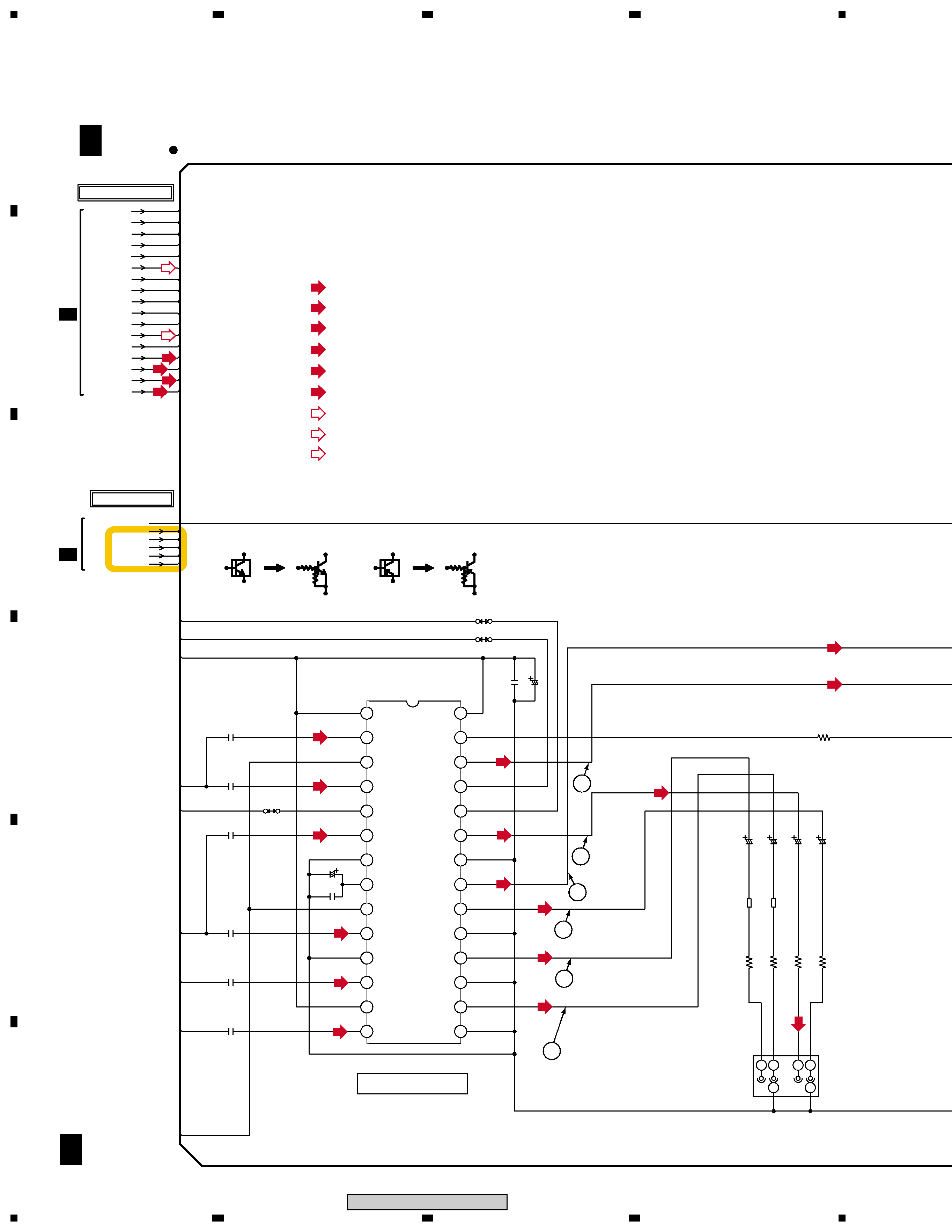
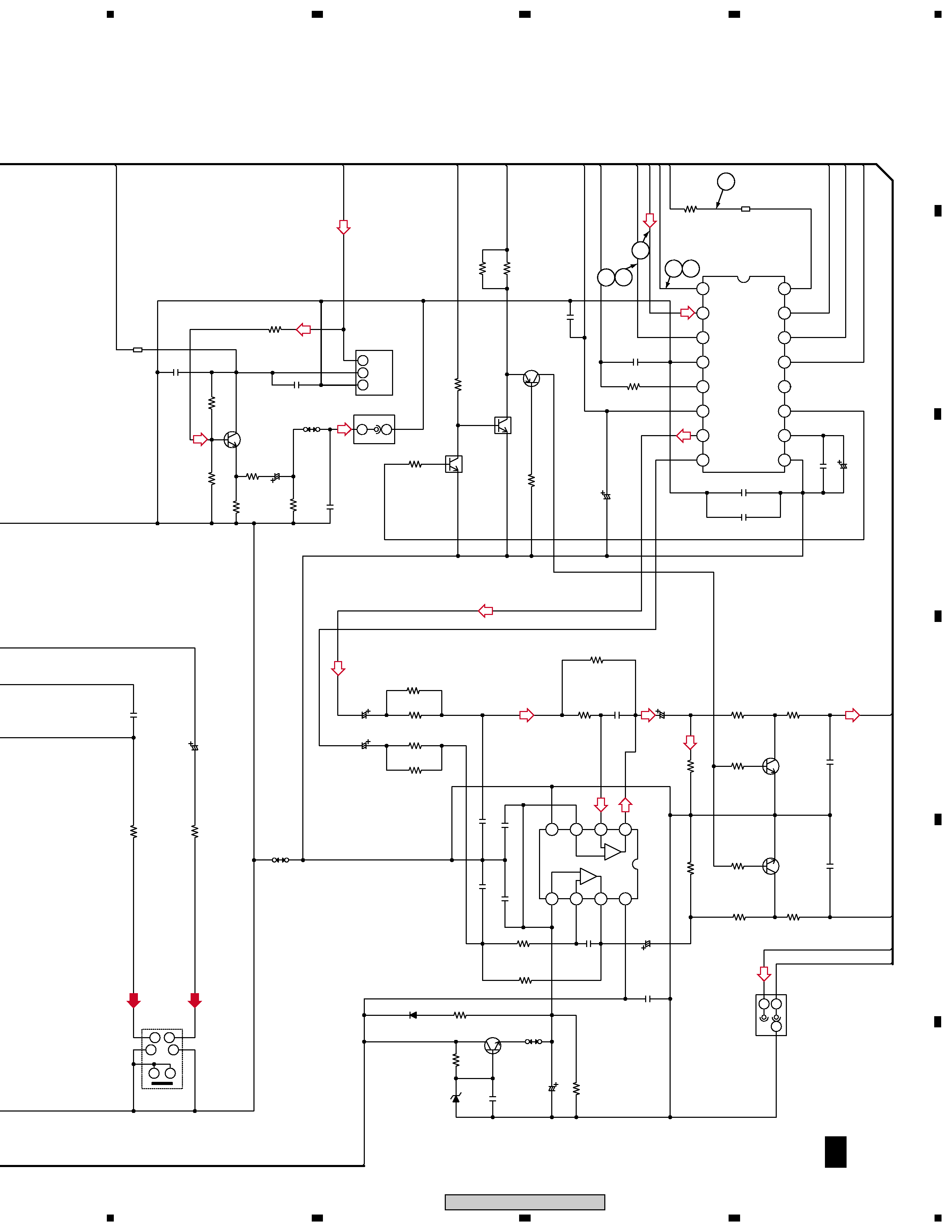
DVD MT PCB ASSY (A2G512A130)
AUDIO/VIDEO JACK BLOCK
1/5
A
5/5
A
: VIDEO SIGNAL ROUTE
(SY)
: S VIDEO SIGNAL ROUTE (Y ch)
(SC)
: S VIDEO SIGNAL ROUTE (C ch)
(R/CR)
: VIDEO SIGNAL ROUTE (R/CR ch)
(G/Y)
: VIDEO SIGNAL ROUTE (G/Y ch)
(B/CB)
: VIDEO SIGNAL ROUTE (B/CB ch)
(D)
: AUDIO DATA SIGNAL ROUTE
(DA)
: AUDIO SIGNAL ROUTE (Digital)
: AUDIO SIGNAL ROUTE (L ch)
(R/CR)
(G/Y)
(B/CB)
(D)
(DA)
(SY)
(SC)
(R/CR)
(G/Y)
(B/CB)
(R/CR)
(G/Y)
(B/CB)
(SC)
(SC)
(SY)
(SY)
12
10
11
9
14
13
A F4/5
A F4/5
2. SCHEMATIC DIAGRAM
Note : When ordering service parts, be sure to refer to "EXPLODED VIEWS and PARTS LIST" or "PCB PARTS LIST"
2.1 DVD MT PCB ASSY
5
1
23
4
1
2
3
4
C
D
F
A
B
E
DV-3800-S
IC8004
PCM1742KEG/2K
AUDIO DAC 2CH
1
10
11
12
13
14
15
16
2
3
4
5
6
7
8
9
J8002
MDC-070V-B_LF
Y/C SEPA
1
2
3
4
5
6
D8007
1SS355
D8005
UDZS6.8B
Q8013
DTC114YUA
MUTE CTL
Q8010
DTC114YUA
MUTE CTL
H
E
J8004
MSP-251V-05NI-FE-LF
COAXIAL
1
2
H1
H2
E
J8003
MSP-242V2-01NI-FE_LF
L/R AUDIO OUT
1
2
3
Q8005
KTC3875S_Y_RTK
COAXIAL DRIV
Q8018
2SD2114K
MUTE SW
Q8019
2SD2114K
MUTE SW
Q8016
KTC3875S_Y_RTK
REF GEN
Q8014
KTA1504S_Y_RTK
JACK MUTE CTL
C8007
0.0022
B
C8068
0.1
B
C8075
0.1
B
C8036
1B
C8042
100P
CH
C8069
100P CH
C8056
560P
CH
C8058
0.1
B
C8059
0.1
B
C8057
560P
CH
C8067
100P
CH
C8021
0.1
B
C8077
330P
CH
C8078
330P
CH
C8074
0.001
B
C8008
0.1
B
C8062
1B
C8072
0.1
B
C8076
100
10V
YK
C8038
1
50V
KA
C8073
47
16V
YK
C8053
100
10V
YK
C8051
100
10V
YK
C8070
47
16V
YK
C8025
470
6.3V
YK
C8061
1000
6.3V
YK
C8066
100
10V
YK
R8065
10
R8070
33
R8046
2.2K
R8038
220
R8036
3.9K
R8037
1.8K
R8035
2.2K
R8044
10K
R8040
100K
R8039
68
R8066
10K
+-1%
R8067
18K
+-1%
R8059
10K
+-1%
R8060
270K
R8048
270K
R8049
10K
+-1%
R8061
10K
+-1%
R8063
18K
+-1%
R8023
75
+-1%
R8026
75
+-1%
R8073
22K
R8074
22K
R8080
220
+-1%
R8085
220
+-1%
R8079
220
+-1%
R8084
220
+-1%
R8081
470
R8078
470
R8051
3.9K
R8052
3.9K
R8056
4.7K
R8069
680K
R8054
2.2K
R8057
100
IC8003
BA4560F-E2
AUDIO
LPF&
1
2
3
4
5678
W824
W866
W856
B8004
MMZ1608R102CT
B8003
MMZ1608R102CT
SD
SCK
V+5A
V+3A
ALRCK
ABCK
ACLK
V+5V
ASPDIF
XAMUTE
V+12AT
ASDAT0
DAC_XCS0
AUDIO_L
GND
AUDIO_R
AUDIO_L
AUDIO_R
V+12
NC
5V
GND
Vdd
Vcc
MCLK
MC
ML
MD
Vcom
BCKIN
Vout L
Vout R
ZERO L
ZERO R
DATA
LRCKIM
AGND
+
-
-
+
+VS
-VS
LR
C
Y
6.8
12.5
6.3
(DA)
(DA)
(DA)
NOTE : THE DC VOLTAGE EACH PART WAS
MEASURED WITH THE DIGITAL TESTER
DURING PLAYBACK.
R8035
2.2K
ASPDIF
(DA)
OS8001
OFTG038101
OPTICAL
1
2
3
C8037
0.1
B
GND
INPUT
VCC
(DA)
(SC)
(DA)
(D)
(D)
3
4 7
8
6
5
(SY)
A F4/5