ORDER NO.
PIONEER CORPORATION 4-1, Meguro 1-chome, Meguro-ku, Tokyo 153-8654, Japan
PIONEER ELECTRONICS (USA) INC. P.O. Box 1760, Long Beach, CA 90801-1760, U.S.A.
PIONEER EUROPE NV Haven 1087, Keetberglaan 1, 9120 Melsele, Belgium
PIONEER ELECTRONICS ASIACENTRE PTE. LTD. 253 Alexandra Road, #04-01, Singapore 159936
PIONEER CORPORATION 2004
RRV2952
DVD PLAYER
DV-3700-G
Model No.
Order No.
Remarks
DV-373-S/RRXCN
RRV2950
¶ This service manual should be used together with the following manual(s):
THIS MANUAL IS APPLICABLE TO THE FOLLOWING MODEL(S) AND TYPE(S).
Model
Power Requirement
Region No.
Serial No.
Confirm 3rd & 4th
alphabetical letters.
DV-3700-G
AC110-127V/220-240V
6
&&TE######$$
Type
RAXCN
T ZZE MAY 2004 Printed in Japan
1
23
4
C
D
F
A
B
E
2
12
3
4
DV-3700-G
1. CONTRAST OF MISCELLANEOUS PARTS
Parts marked by "NSP" are generally unavailable because they are not in our Master Spare Parts List.
The
mark found on some component parts indicates the importance of the safety factor of the part.
Therefore, when replacing, be sure to use parts of identical designation.
Screws adjacent to
mark on product are used for disassembly.
For the applying amount of lubricants or glue, follow the instructions in this manual.
(In the case of no amount instructions, apply as you think it appropriate.)
NOTES:
When ordering resistors, first convert resistance values into code form as shown in the following examples.
Ex.1 When there are 2 effective digits (any digit apart from 0), such as 560 ohm and 47k ohm (tolerance is shown by J=5%,
and K=10%).
Ex.2 When there are 3 effective digits (such as in high precision metal film resistors).
561
473
R50
1R0
5621
560
47k
0.5
1
RD1/4PU
J
RD1/4PU
J
RN2H
K
RS1P
K
56
x 10 1
47
x 10 3
R50
1R0
561
473
5.62k
RN1/4PC
F
562
x 10 1
5621
7 CONTRAST TABLE
DV-3700-G/RAXCN and DV-373-S/RDXCN/RA are constructed the same except for the following:
PCB ASSEMBLIES
P9 - 1
1..DVDM Assy
VWS1575
VWS1577
NSP
1..FLKB Assy
VWM2244
VWM2246
P11 - 1
2..FLKY Assy
VWG2479
VWG2481
P11 - 2
2..PWSB Assy
VWG2482
VWG2482
PACKING
P7 - 1
>
Power Cable
ADG1158
ADG7079
P7 - 7
Operating Instructions (English)
VRB1330
Not used
P7 -16
Packing Case
VHG2463
VHG2466
P7 -20
NSP
Warranty Card
ARY7025
ARY7046
Operating Instructions (Simp-Chinese)
Not used
VRC1190
EXTERIOR SECTION
P9 -10
Bonnet
VNA2677
VNA2679
P9 -13
Rear Sheet
VRW2030
VRW2026
P9 -14
DVD-V Plate
VAM1135
VAM1123
P9 -15
Tray Panel
VNK5411
VNK5412
P9 -16
Caution Label
VRW1872
VRW1904
FRONT PANEL SECTION
P11 - 4
Pioneer Name Plate
VAM1129
VAM1112
P11 - 7
Front Panel
VNK5476
VNK5402
P11 - 8
Main Key
VNK5404
VNK5405
P11 - 9
Key Top
VNK5407
VNK5408
Ref.
No.
Remarks
DV-373-S/RDXCN/RA
DV-3700-G/RAXCN
Part No.
Mark
Symbol and Description
· For PCB Assemblies, Refer to "CONTRAST OF PCB ASSEMBLIES" and "2. SCHEMATIC DIAGRAM".
5
67
8
3
5
6
7
8
DV-3700-G
C
D
F
A
B
E
7 CONTRAST OF PCB ASSEMBLIES
F
C
IC603
VYW2238
VYW2237
Mark
Symbol and Description
Part No.
VWS1575
VWS1577
Remarks
R189
Not used
RS1/16S103J
R190
RS1/16S103J
Not used
Mark
Symbol and Description
Part No.
VWG2479
VWG2481
Remarks
FLKY Assy
VWG2481 and VWG2479 are constructed the same except for the following:
B DVDM Assy
VWS1577 and VWS1575 are constructed the same except for the following:
1
23
4
C
D
F
A
B
E
4
12
3
4
DV-3700-G
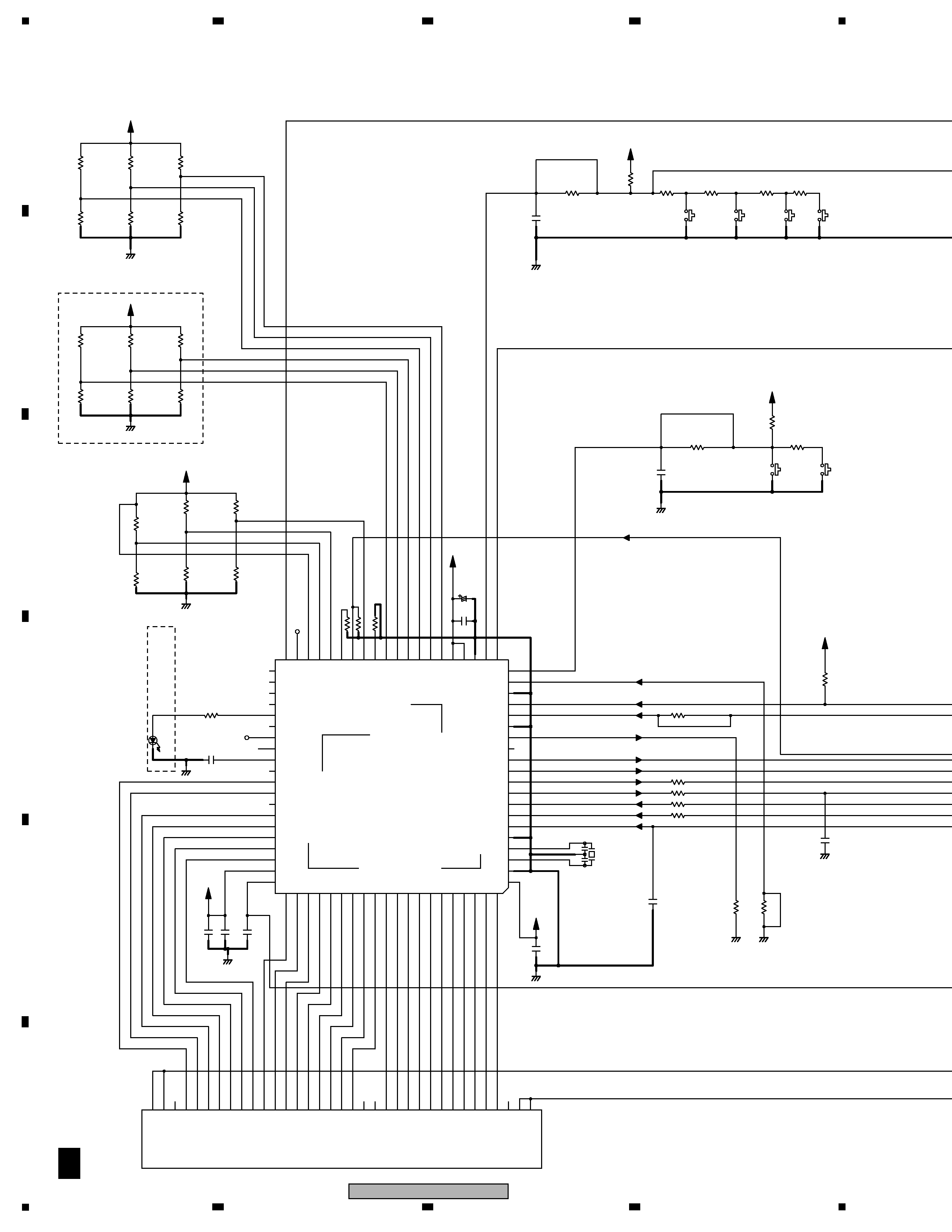
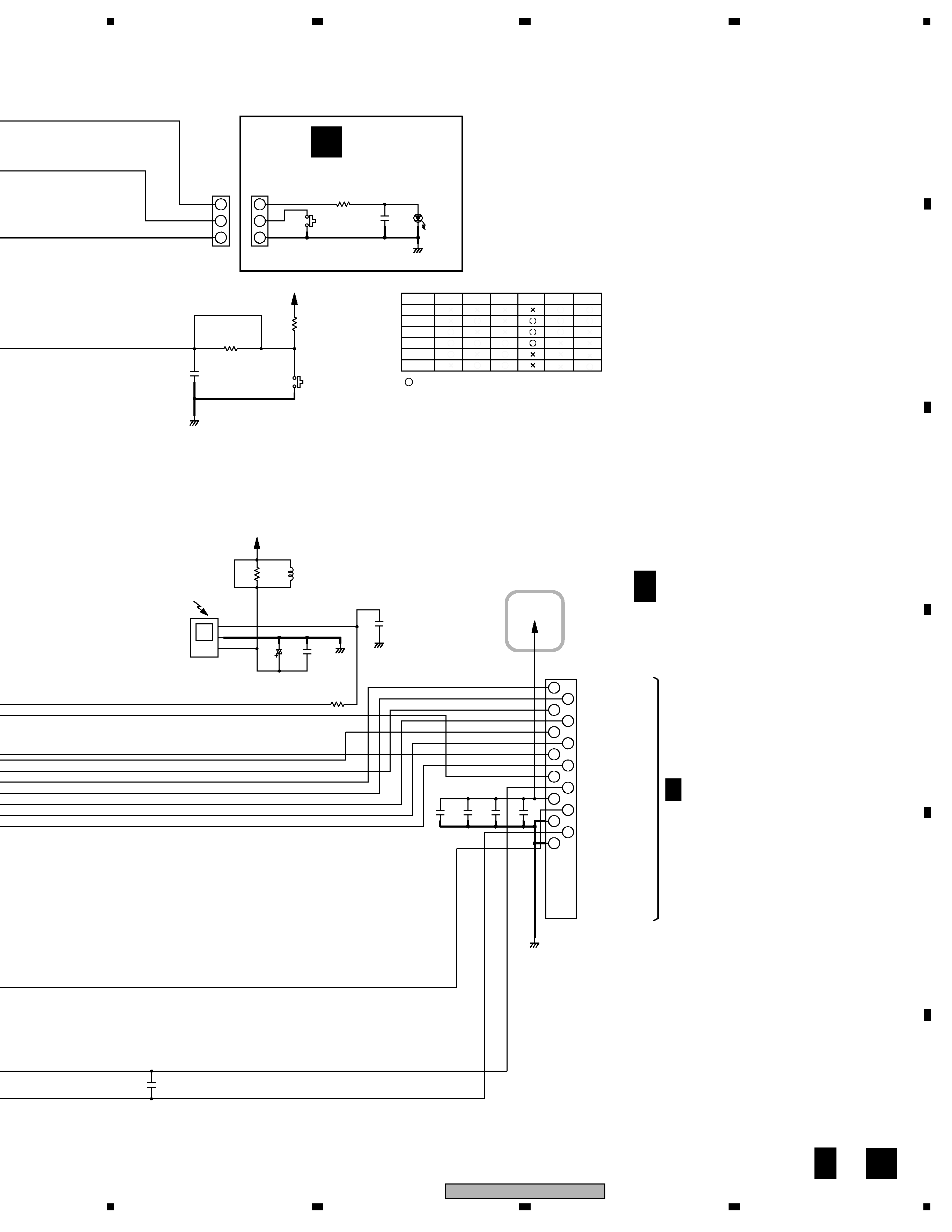
2. SCHEMATIC DIAGRAM
C F
GND
***
***
0.1/50V
V+3E
***
SLR-343VC(NPQ)-TS
GND
***
***
GND
0.1
V+3E
GND
GND
(5MHz)
VSS1142-
1000p
***
***
***
GND
PE5374B
47
47
0
47
***
***
***
GND
10k
10k
0
***
***
V+3E
GND
V+3E
10k
10k
10k
0.1
***
V+3E
V+3E
0.01
GND
YB
***
10K
1.2k
V+3E
GND
***
10k
10k
10k
***
V+3E
***
GND
0.01
YB
1.2k
2.2k
2.7k
3.9k
***
***
10K
V+3E
V101
C159
C103
C104
D102
C184
R134
C105
X101
C183
R140
R199
C128
IC101
R130
R129
R128
R127
R123
R183
R195
R112
R110
R111
R196
R109
R186
R190
R188
R185
R189
R187
R139
R135
R136
C102
C101
C153
S105
R178
R173
R152
R104
R106
R108
R103
R107
R105
C151
S119
S107
S103
R177
R172
R160
R155
R154
R159
S108
S106
FL+
FL+
P16
P13
P12
P11
P14
P15
P8
P7
P6
P9
P10
FL TUBE
P1
NC
P4
P5
P3
P2
G10
NC
G7
G11
G9
G8
G5
G6
G1
G2
FL-
FL-
G3
G4
P9
P8
P7
P10
P11
P12
NC
P14
P13
P15
1394RST
P16
NC
TEST0
TEST1
[FL
DIMMER]
(RED)
STBY
LED
TEST2
FL
SET1
LED0
LED1
P1
P6
P5
P4
P3
P2
G7
G11
G10
G9
G8
60 -28V
59 VDD
G2
G1
G3
G4
G5
G6
1 VDD
X1
GND
X2
IC
1394POWER ON
22
KEY0
21
KEY1
41 LED5
42 LED4
43 LED3
FL CONTROL
MICROCOMPUTER
44 LED2
SO
RESET IN
SI
SCK
XREADY
POWER ON
RESET OUT
RESERVE OUT
NOR/KARAOKE
CHECKER
FL
SET2
ON
POWER
MS0_0
MS0_1
MS1_2
MS1_1
MS1_0
TES
OEM
HALT
SEL IR
GND
ACK
MS0_2
KEY2
ECHO
VDD
VDD
GND
Note1
[EJECT]
[STOP]
KEY1
KEY2
KEY0
[PLAY]
[>>] [FL DIM]
[<<]
32
34
35
33
29 28 27
30
31
24 23 22
26
21
25
20
15
16
17
18
19
13 12
14
10
11
2
4
76
98
1
3
5
62
60
61
63
59
57
56
55
58
53
52
54
51
49
47
50
48
43
46
44
45
39
42
41
40
67
64 65 66
68 69
73
72
75
71
70
74
77
80
79
78
76
1
2
3
6
4
5
10
8
9
7
13
12
11
14
38
37
36
35
33
34
28
32
29
27
31
30
16
15
18
17
22
26
23
21
25
24
20
19
VAW1078-
VAW1076-
2.1 FLKY and PWSB ASSYS
5
67
8
5
5
6
7
8
DV-3700-G
C
D
F
A
B
E
D
C F
***
GND
0
***
0.1
GND
***
***
***
***
GND
RPM7240-H4
***
***
V+3E
***
V+3E
0.01
GND
***
YB
V+3E
10K
***
GND
***
***
C106
R184
C182
C181
C156
C155
C158
C157
CN101
IC104
C199
L101
R181
C152
S117
R176
R171
CN102
CN103
S101
C154
R138
D105
ALL TACT SWITCHES = VSG1024- -T
*** : parts not mounted
FLDC-
GND
GND
-28V
FLDC+
V+3E
XNOR/KARAOKE
ACK
RESET
SCK
XRESET
S(MtoF)
POWER ON
S(FtoM)
XREADY
[PAUSE]
: 10K
(resistor)
R189
R186
R190
R188
R187
R185
RPW, RR
Note1
JJ
WY
RT
RA
LF
[POWER]
14
3
1
12
11
10
13
8
7
6
9
5
4
3
1
2
2
1
3
2
1
3
2
REMOTE
RECEIVER
15
CN105
B 2/4
D
PWSB ASSY
(VWG2482)
FLKY ASSY
S105 :
OPEN/CLOSE
S106 :
S107 :
S108 :
S117 :
S119 :
PWSB ASSY
S101 :
STANDBY/ON
FLKY ASSY
(VWG2481)
C F