ORDER NO.
PIONEER CORPORATION 4-1, Meguro 1-chome, Meguro-ku, Tokyo 153-8654, Japan
PIONEER ELECTRONICS SERVICE, INC. P.O. Box 1760, Long Beach, CA 90801-1760, U.S.A.
PIONEER EUROPE NV Haven 1087, Keetberglaan 1, 9120 Melsele, Belgium
PIONEER ELECTRONICS ASIACENTRE PTE. LTD. 253 Alexandra Road, #04-01, Singapore 159936
PIONEER CORPORATION 2000
RRV2336
DVD PLAYER
T ZZE JULY 2000 Printed in Japan
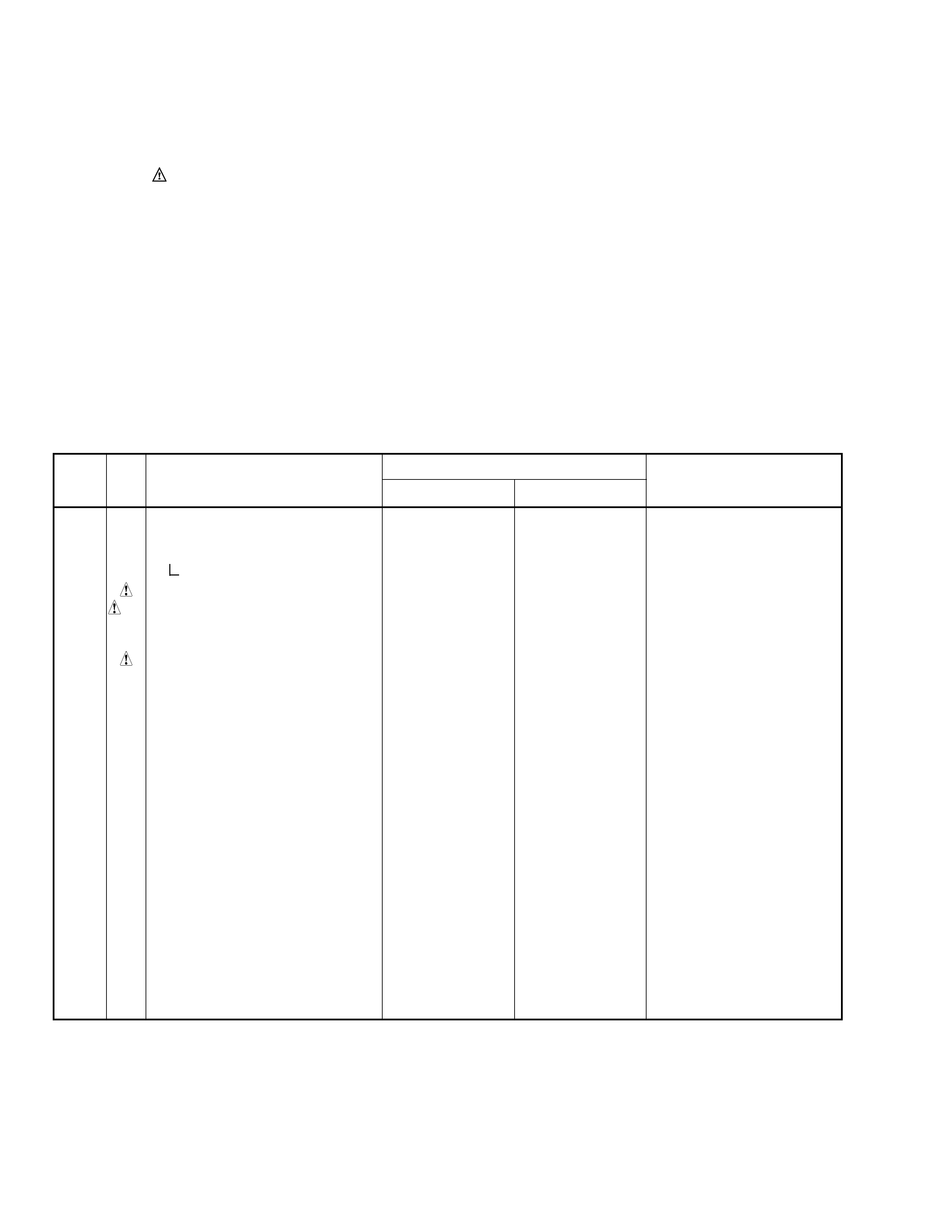
Model No.
Order No.
Remarks
DV-333/KUXQ
RRV2290
¶ This service manual should be used together with the following manual(s):
DV-3300
Type
Power Requirement
Model
DV-3300
THIS MANUAL IS APPLICABLE TO THE FOLLOWING MODEL(S) AND TYPE(S).
Region No.
RAMXQ
AC110-127/220-240V
6
Automatic select
The voltage can be converted by
the following method.
1. CONTRAST OF MISCELLANEOUS PARTS .......... 2
2. SCHEMATIC DIAGRAM .......................................... 4
3. PCB CONNECTION DIAGRAM ........................... 13
CONTENTS
DV-3300
2
7 CONTRAST TABLE
DV-3300/RAMXQ and DV-333/KUXQ are constructed the same except for the following:
PCB ASSEMBLIES
P5 - 1
DVDM Assy
VWS1412
VWS1413
FLJB Assy
VWM1991
VWM2051
P5 - 4
FLJB Assy
VWV1748
VWV1782
P5 - 5
POWER SUPPLY Unit
VWR1327
VWR1330 (
1)
P5 - 5
NSP
POWER SUPPLY Unit
VWR1328
VWR1331 (
1)
PACKING
P3 - 1
Power Cord
ADG7022
ADG7018
P3 - 9
Packing Case
VHG1903
VHG1935
P3 -11
NSP
Warranty Card
ARY7045
ARY7046
P3 -13
Operating Instructions (English)
VRB1244
Not used
P3 -13
Operating Instructions (Simp-Chinese)
Not used
VRC1113
EXTERIOR
P5 -12
Rear Panel
VNA2174
VNA2196
P5 -13
Tray
VNL1858
VNL1884
P5 -15
Pioneer Name Plate
VAM1099
VAM1100
P5 -16
Tray Panel
VNK4591
VNK4592
P5 -17
Front Panel Assy
VXA2407
VXA2406
P5 -18
NSP
Label
VRW1629
Not used
P5 -19
NSP
Pop Label
VRW1830
VRW1832
P5 -20
Bonnet S
VXX2651
VXX2652
P5 -24
Screw
BCZ40P060FZK
BCZ40P060FNI
P5 -26
FL Lens
VNK4593
VNK4734
Label
Not used
VRW1699
For Bonnet
Label
Not used
VRW1739
For Rear Panel
Ref.
No.
Remarks
DV-333/KUXQ
DV-3300/RAMXQ
Part No.
Mark
Symbol and Description
1. CONTRAST OF MISCELLANEOUS PARTS
· For PCB assemblies, Refer to "CONTRAST OF PCB ASSEMBLIES", "PCB PARTS LIST", "2. SCHEMATIC DIAGRAM" and "3. PCB
CONNECTION DIAGRAM".
1 : As for POWER SUPPLY Unit, either VWR1330 or VWR1331 is installed. Install VWR1330 when replacing the POWER SUPPLY Unit.
NOTES :
÷ Parts marked by " NSP " are generally unavailable because they are not in our Master Spare Parts List.
÷ The
mark found on some component parts indicates the importance of the safety factor of the part.
Therefore, when replacing, be sure to use parts of identical designation.
÷ Reference Nos. indicate the pages and Nos. in the service manual for the base model.
÷ When ordering resistors, first convert resistance values into code form as shown in the following examples.
Ex. 1
When there are 2 effective digits (any digit apart from 0), such as 560 ohm and 47k ohm (tolerance is shown by
J = 5%, and K = 10%).
560
= 56 × 101= 561 ................................................... RD1/4PU 5 6 1 J
47k
= 47 × 10 3 = 473 .................................................. RD1/4PU 4 7 3 J
0.5
= R50 ...................................................................... RN2H Â 5 0 K
1
= 1R0 ......................................................................... RS1P 1 Â 0 K
Ex. 2
When there are 3 effective digits (such as in high precision metal film resistors).
5.62k
= 562 × 10 1 = 5621 ........................................... RN1/4PC 5 6 2 1 F
DV-3300
3
7 CONTRAST OF PCB ASSEMBLIES
IC13
VYW1727
VYW1700
R1
Not used
RS1/16S103J
For CHECKER
R2
RS1/16S103J
RS1/16S333J
For CHECKER
R882
Not used
DCN1106 (0
)
R951R955
Not used
RS1/16S0R0J
Mark
Symbol and Description
Part No.
VWS1412
VWS1413
Remarks
DVDM ASSY
VWS1413 and VWS1412 are constructed the same except for the following:
F
D
S401
Not used
VSH1020
R118
RS1/10S220J
RS1/10S180J
R119
RS1/10S220J
RS1/10S330J
R140
RS1/10S0R0J
RS1/10S273J
R141
RS1/10S622J
RS1/10S163J
R142
Not used
RS1/10S683J
R143
RS1/10S363J
RS1/10S272J
R486
RS1/10S682J
Not used
R487
Not used
RS1/10S682J
R488
Not used
RS1/10S153J
R489
Not used
RS1/10S103J
Mark
Symbol and Description
Part No.
VWV1748
VWV1782
Remarks
FLJB ASSY
VWV1782 and VWV1748 are constructed the same except for the following:
F
E
7 PCB PARTS LIST
POWER SUPPLY UNIT (VWR1330)
OTHERS
P101 PROTECTOR (800mA)
AEK7063
P102 PROTECTOR (1.6A)
AEK7066
FU101 FUSE (2.5A)
REK1102
POWER SUPPLY UNIT (VWR1331)
OTHERS
P101 PROTECTOR (630mA)
VZE1001
P102 PROTECTOR (1.25A)
VZE1003
P103 PROTECTOR (1.6A)
VZE1004
Mark No.
Description
Part No.
F
I
F
I
Note : When the fuse(F001) on VWR1331 blow out, VWR1331 might
be damaged.
At that time, exchange VWR1331 for VWR1330.
DV-3300
4
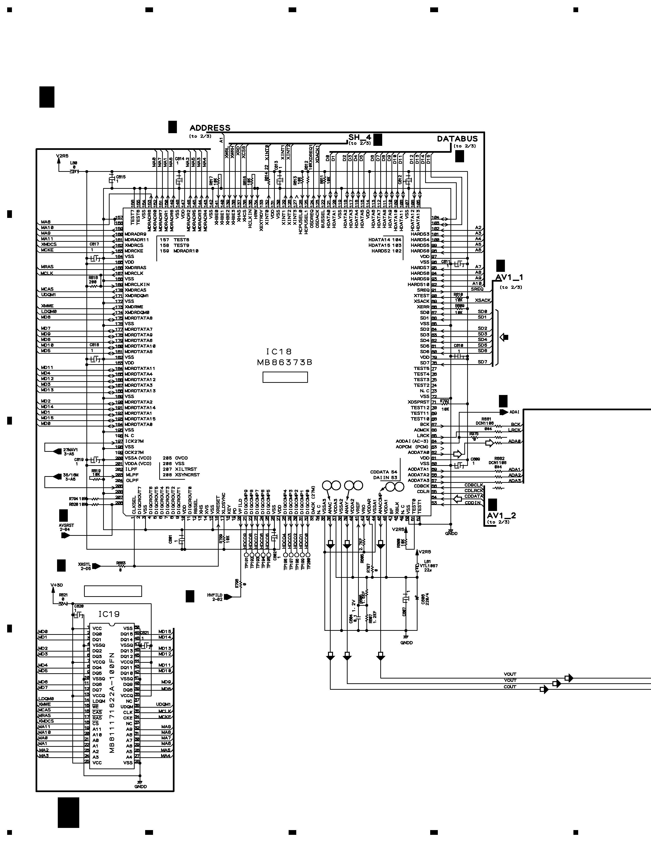
A
B
C
D
1
23
4
12
3
4
AV-1
16M SDRAM
2/3
D
2/3
D
2/3
D
2/3
D
2/3
D
2/3
D
2/3
D
2/3
D
2/3
D
D 3/3F DVDM ASSY (VWS1413)
(VCB)
(Y)
(C)
(VCB)
(Y)
(C)
(VCB)
(Y)
(C)
13 16
12 15
14 17
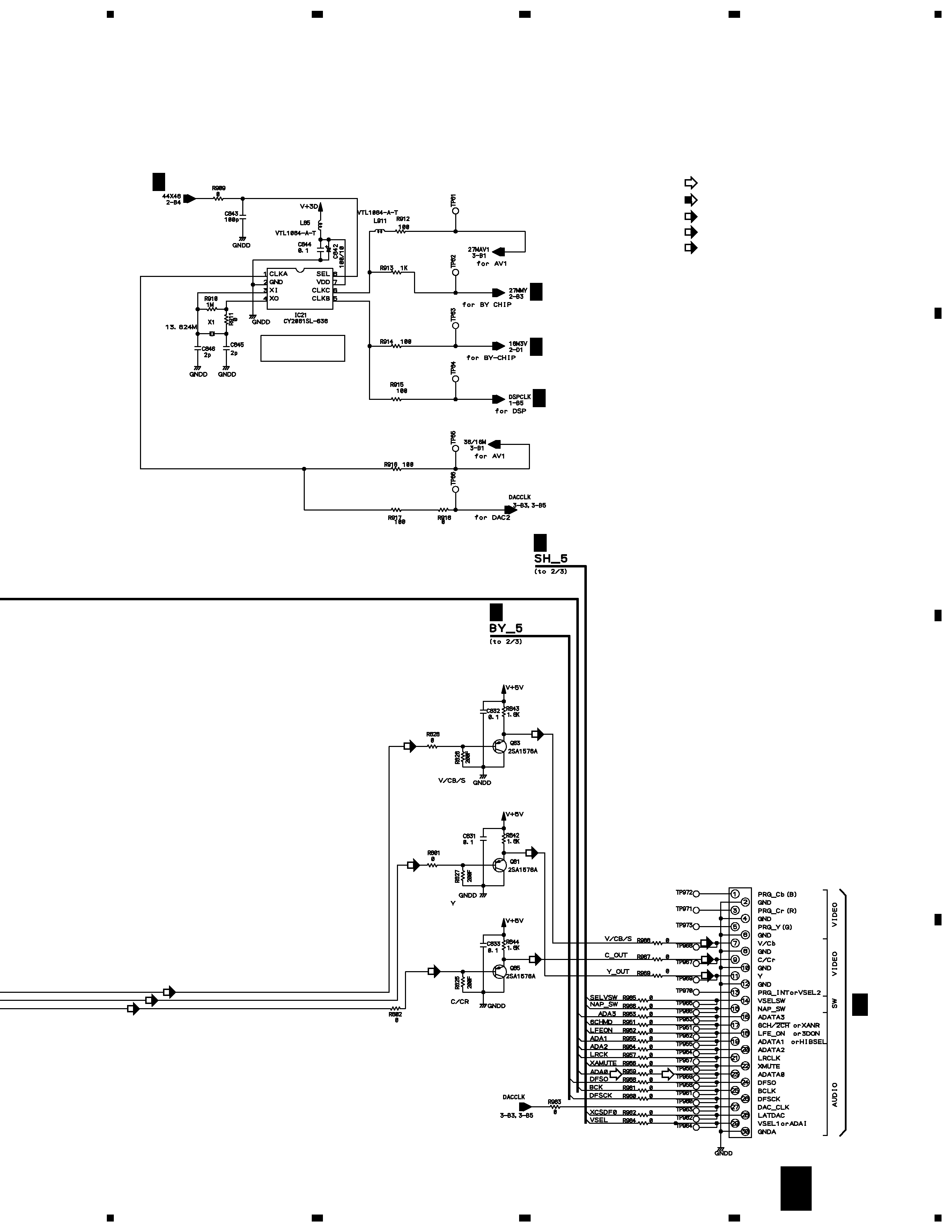
2.1 DVDM ASSY (3/3)
3/3F
D
2. SCHEMATIC DIAGRAM
DV-3300
5
A
B
C
D
5
67
8
5
6
7
8
CLOCK
GENERATOR
CN15
VKN1763
2/3
D
2/3
D
2/3
D
2/3
D
2/3
D
1/3
D
CN106
E 3/3F
: AUDIO SIGNAL ROUTE
: ROM DATA SIGNAL ROUTE
: V/CB SIGNAL ROUTE
(VCB)
: Y SIGNAL ROUTE
(Y)
: C SIGNAL ROUTE
(C)
(VCB)
(Y)
(C)
(VCB)
(VCB)
(VCB)
(Y)
(Y)
(Y)
(C)
(C)
(C)
3/3F
D
Note : When ordering service parts, be sure to refer to "EXPLODED VIEWS and PARTS LIST" or "PCB PARTS LIST".