PIONEER CORPORATION
4-1, Meguro 1-Chome, Meguro-ku, Tokyo 153-8654, Japan
PIONEER ELECTRONICS (USA) INC.
P.O.Box 1760, Long Beach, CA 90801-1760 U.S.A.
PIONEER EUROPE NV
Haven 1087 Keetberglaan 1, 9120 Melsele, Belgium
PIONEER ELECTRONICS ASIACENTRE PTE.LTD. 253 Alexandra Road, #04-01, Singapore 159936
C PIONEER CORPORATION 2002
K-ZZA. JAN. 2002 Printed in Japan
ORDER NO.
CRT2820
Service
Manual
Model
Service Manual
CD Mechanism Module
DEH-P740MP/XN/UC
CRT2783
CXK5555
DEH-P7400MP/XN/UC
DEH-P7450MP/XN/ES
DEH-P7400MP/XN/EW
CRT2784
CD MECHANISM MODULE
CX-3007
- This service manual describes the operation of the CD mechanism module incorporated in models
listed in the table below.
- When performing repairs use this manual together with the specific manual for model under repair.
CONTENTS
1. CIRCUIT DESCRIPTIONS ...........................................2
2. MECHANISM DESCRIPTIONS.................................18
3. DISASSEMBLY .........................................................20
2
CX-3007
1. CIRCUIT DESCRIPTIONS
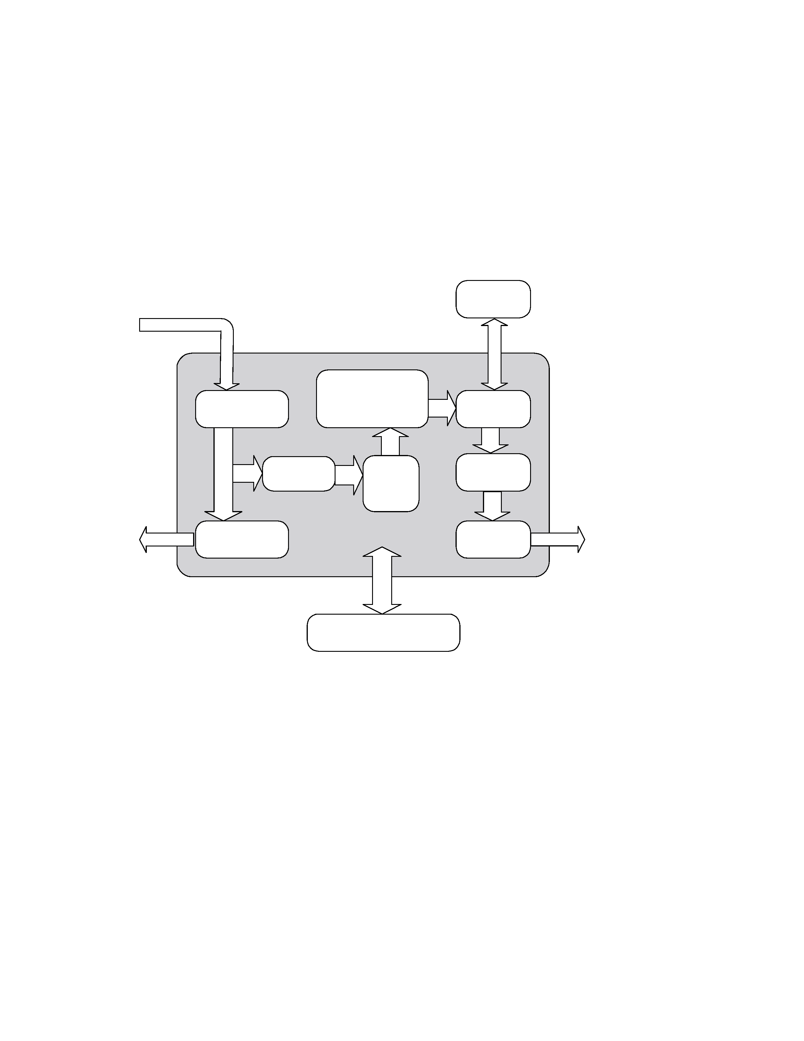
Recently, most CD LSI's have included DAC, RF amplifier and other peripheral circuits, as well as the core circuit DSP.
This series of mechanisms employ a multi-task LSI UPD63760GJ, which has CD-ROM decoder and MP3 decoder in
addition to the CD block as shown in the Fig.1.0.1. This enables to reproduce a CD-ROM where MP3 data is recorded.
Plus, in this lineup, there are WMA supported models available where WMA decoder UPD61002GC is added.
CXK5555 --- WMA non-supported
CXK5556 and CXK5557 --- WMA supported
Fig.1.0.1 Block diagram of CD LSI UPD63760GJ
CD-ROM
DECODER
BMC
EFM
MP3
DECODER
DAC
DRAM
UCOM
A - F
UPD63760GJ
SIGNAL
PROC-
ESSOR
RF
AMPLIFIER
DRIVE
OUTPUT
DIGITAL
SERVO
AUDIO
OUTPUT
3
CX-3007
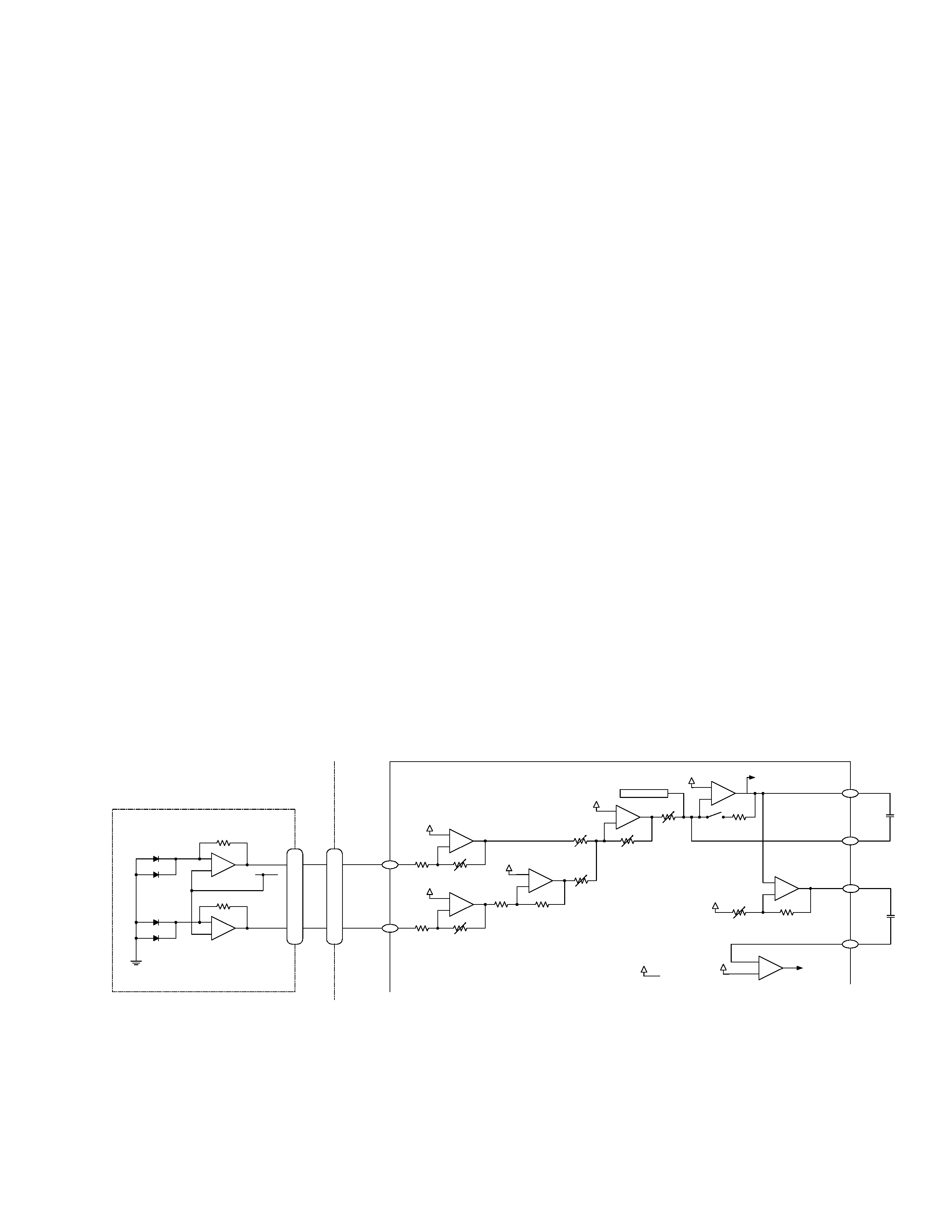
1.1 PREAMPLIFIER BLOCK (UPD63760GJ: IC201)
In the preamplifier block, the pickup output signals are processed to generate signals that are used for the next-stage
blocks: the servo block, demodulator, and control.
After I/V-converted by the preamplifier with built-in photo detectors (inside the pickup), the signals are applied to the
preamplifier block in the CD LSI UPD63760GJ (IC201). After added by the RF amplifier in this block, these signals are
used to produce necessary signals such as RF, FE, TE, and TE zero-cross signals.
The CD LSI employs a single power supply system of + 3.3V. Therefore, the REFO (1.65V) is used as the reference
voltage both for this CD LSI and the pickup. The LSI produces the REFO signal by using the REFOUT via the buffer
amplifier and outputs from the pin 131. All the measurements should be made based on this REFO.
Caution: Be careful not to short the REFO and GRD when measuring.
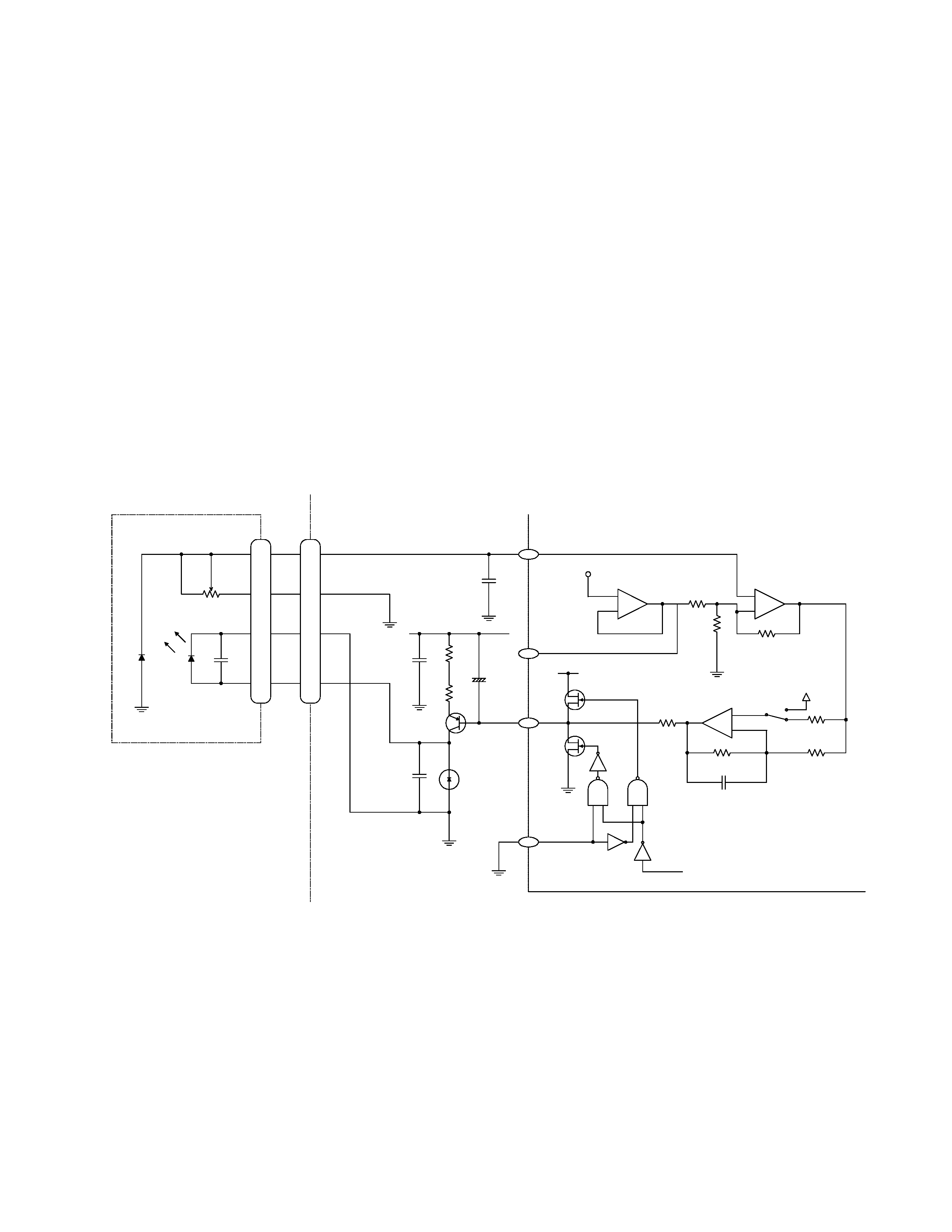
1.1.1 APC (Automatic Power Control)
A laser diode has extremely negative temperature characteristics in optical output at constant-current drive. To keep
the output constant, the LD current is controlled by monitor diodes. This is called the APC circuit. The LD current is
calculated at about 30mA, which is the voltage between LD1 and V3R3D divided by 7.5 (ohms).
Fig. 1.1.1 APC
6R5K
+
-
1K
100K
+
-
6R5K
100K
+
-
110K
1K
REG 1R25V
Vref
3P
142
143
140
PD
PN
LDREGO
LD
UPD63760GJ
141
+
R001
R1
R1
5
7
15
5
7
15
14
14
PICKUP UNIT
UNIT
1R5
x
5
2SB1132
1SS355
100/16
LD-
LD+
MD
VR
LDS
APN
4
CX-3007
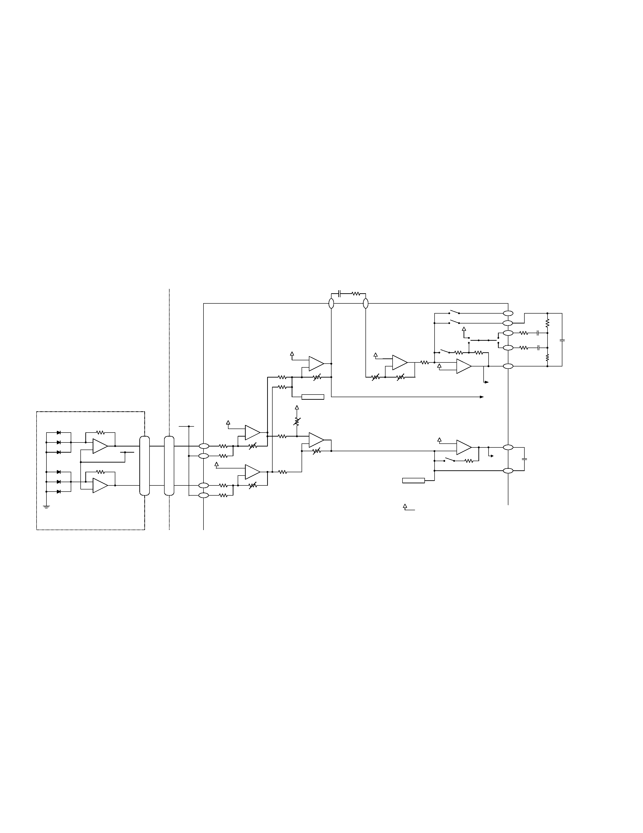
1.1.2 RF and RFAGC amplifiers
The photo-detector outputs (A + C) and (B + D) are added, amplified, and equalized inside this LSI, and then provided
as the RF signal from the RFI terminal. The RF signal can be used for eye-pattern check.
The low frequency component of the RFO voltage is:
RFO = (A + B + C + D) x 2
The RFO is used for the FOK generation circuit and RF offset adjustment circuit.
The RFI output from the pin 118 is A/C-coupled outside this LSI, and returned to the pin 117 of this LSI. The signal is
amplified in the RFAGC amplifier to obtain the RFAGC signal. This LSI is equipped with the RFAGC auto-adjustment
function as explained below. This function automatically controls the RFO level to keep at 1.5V by switching the
feedback gain for the RFAGC amplifier.
The RFO signal is also used for the EFM, DFCT, MIRR, and RFAGC auto-adjustment circuits.
Fig. 1.1.2 RF/AGC/FE
13
6
A+C
B+C
VREF
13
6
10k
10k
8R8K
10K
10K
8R8K
61R0K
61R0K
111K
R2
15R2K
15R2K
35K
18K
20K
11R2K
7R05K
10K
10K
124
127
125
126
121
122
119
120
116
134
133
RFOFF SETTING
RFOFF SETTING
VREF
VREF
A
B
C
D
RFO
AGCI
RF2-
RF-
EQ2
EQ1
AGCO
FEO
FE-
FE A/D
DEFECT/
A3T DETECTION
RFOK
GENERATION
117
118
+
-
+
-
+
-
+
-
+
-
+
-
-
+
P3
P7
P9
P2
P4
P8
PICKUP UNIT
UNIT
UPD63760GJ
10K
10K
330
1R8K
18P
27P
3P
R01
5
CX-3007
1.1.3 Focus error amplifier
The photo-detector outputs (A + C) and (B + D) are applied to the differential amplifier and the error amplifier to obtain
the (A + C - B - D) signal, which is then provided from the pin 91 as the FE signal.
The low frequency component of the FE voltage is:
FE = (A + C - B - D) x 8.8/10k x 111k/61k x 160k/72k
= (A + C - B - D) x 3.5
The FE output shows 1.5Vp-p S-shaped curve based on the REFO. For the next-stage amplifiers, the cutoff frequency
is 14.6kHz.
1.1.4 RFOK
The RFOK circuit generates the RFOK signal, which indicates focus-close timing and focus-close status during the play
mode, and outputs from the pin 53. This signal is shifted to "H" when the focus is closed and during the play mode.
The DC level of the RFI signal is peak-held in the digital block and compared with a certain threshold level to generate
the RFOK signal. Therefore, even on a non-pit area or a mirror-surface area of a disc, the RFOK becomes "H" and the
focus is closed.
This RFOK signal is also applied to the microcomputer via the low-pass filer as the FOK signal, which is used for
protection and RF amplifier gain switching.
1.1.5 Tracking error amplifier
The photo-detector outputs E and F are applied to the differential amplifier and the error amplifier to obtain the (E - F)
signal, and then provided from the pin 136 as the TE signal.
The low frequency component of the TE voltage is:
FEO = (E - F) x 160k/112k x 90.6k/45.36k x 160k/45.4k
= (E - F) x 5.7
The TE output provides the TE waveform of about 1.3Vp-p based on the REFO. For the next-stage amplifiers, the
cutoff frequency is 21.1kHz.
Fig. 1.1.3 TE
11
9
E
F
VREF
11
9
112K
112K
160K
45R36K
160K
160K
160K
45R36K
90R6K
80K
160K
60K
128
129
TEOFF SETTING
TE A/D
136
135
137
138
PICKUP UNIT
P5
P10
P1
P6
E
F
UPD63760GJ
UNIT
+
-
+
-
+
-
+
-
+
-
+
-
-
+
VREF
INTERNAL
TEC
TEO
TE-
TEC
TE2
68P
6800P