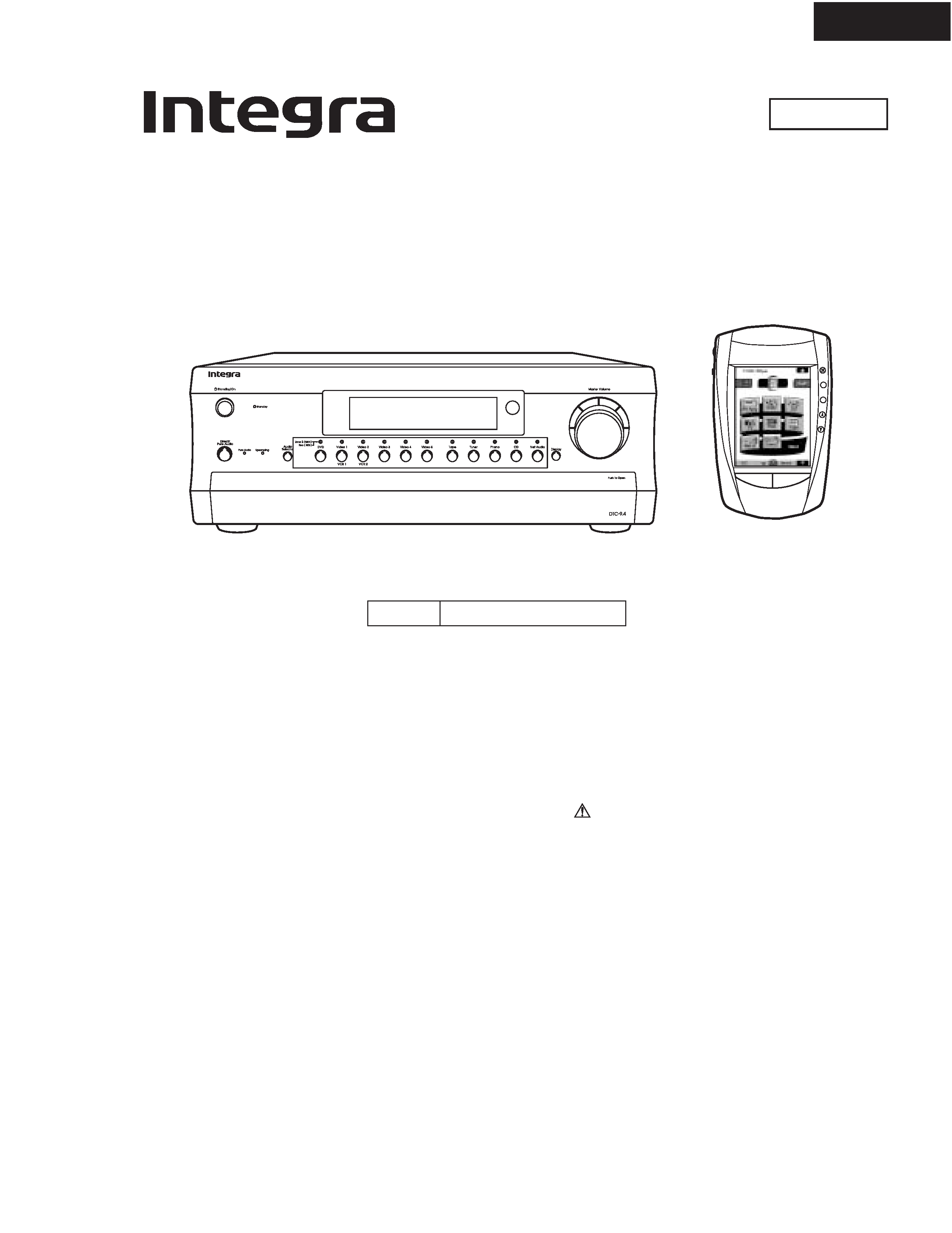
DTC-9.4
SERVICE MANUAL
SERVICE MANUAL
AV CONTROLLER
Black model
MODEL
DTC-9.4
120V AC, 60Hz
BMDD
Ref. No. 3771
Jun, 2003
+
Ð
CH
VOL
MUTE
CONT
+
Ð
LIGHT
SAFETY-RELATED COMPONENT
WARNING!!
COMPONENTS IDENTIFIED BY MARK
ON THE
SCHEMATIC DIAGRAM AND IN THE PARTS LIST ARE
CRITICAL FOR RISK OF FIRE AND ELECTRIC SHOCK.
REPLACE THESE COMPONENTS WITH ONKYO
PARTS WHOSE PART NUMBERS APPEAR AS SHOWN
IN THIS MANUAL.
MAKE LEAKAGE-CURRENT OR RESISTANCE
MEASUREMENTS TO DETERMINE THAT EXPOSED
PARTS ARE ACCEPTABLY INSULATED FROM THE
SUPPLY CIRCUIT BEFORE RETURNING THE
APPLIANCE TO THE CUSTOMER.
DTC-9.4
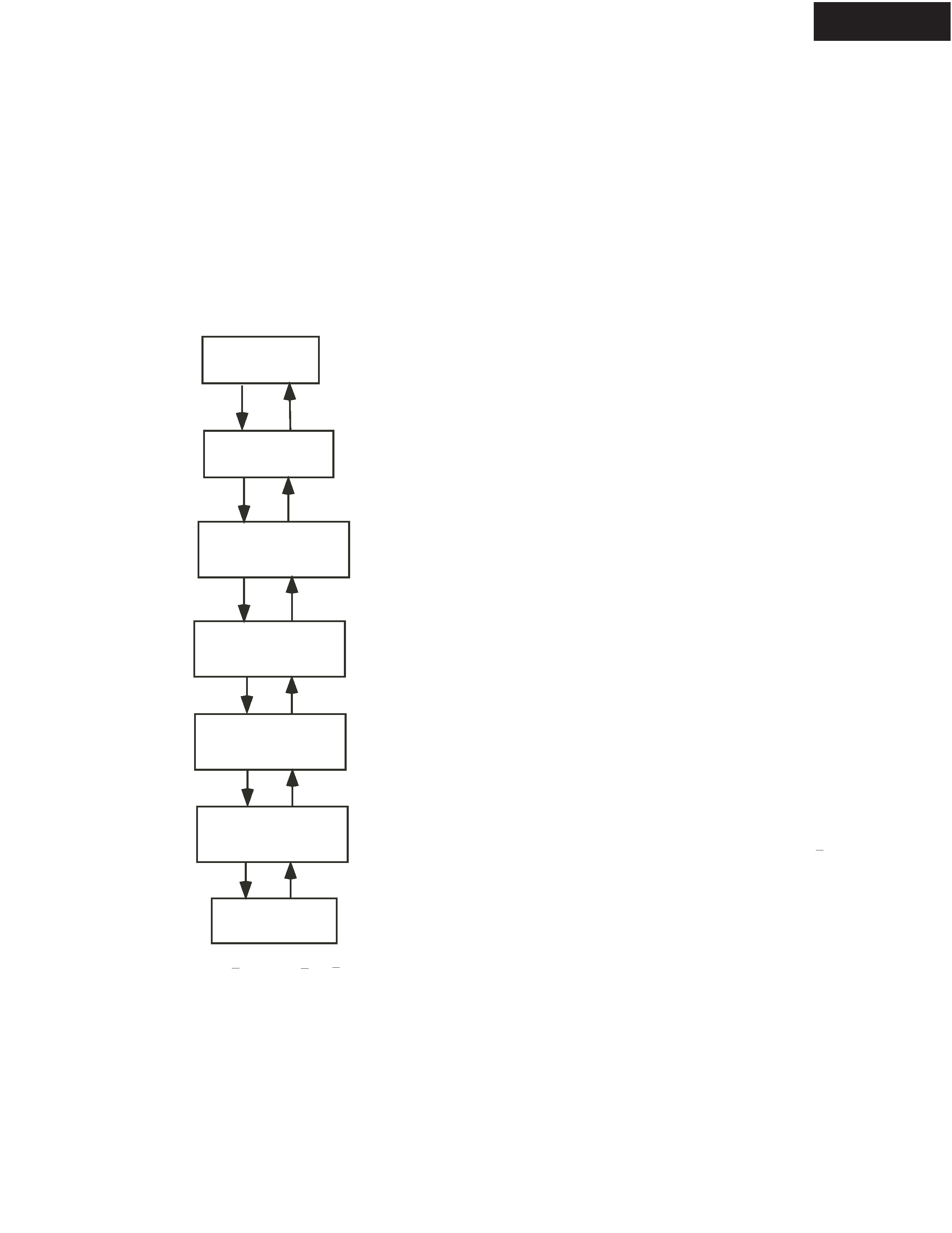
CONFIRMATION PROCEDURES
Test Mode
1. Turn POWER button on.
2. Press and hold down CD button, then press DISPLAY and STANDBY/ON buttons.
3. After "TEST
" on the FL tube is displayed, press CD button to set the unit to the test mode of FL tube.
Note: VIDEO 1:TEST-1 VIDEO 2 :TEST-2
VIDEO 3 :TEST-3 VIDEO 4:TEST-4
The segments of even
number light on .
All segments
light on.
"43210987654321"
light on.
"abcdefghijklmn"
light on.
Test mode of FL tube
ZONE 2....UP
REC OUT......DOWN
REC OUT
ZONE 2
Press POWER button
to finish the test mode of FL tube.
a:Net-tune function "N":avaiable b:Optical input 4 "4":avaiable
c:Tuner aria "U":USA and Canad "E":Europe "W":Worldiwde " ":Japan
d:RDS function "R":avaiable
e:Video format "P":PAL/NTSC auto "N":NTSC
f:3 line Y/C separation function "3":avaiable
g:Video converer function: "C":avaiable
The segments of odd
number light on .
h:12V trigger function "A":A/B/Zone2 "Z":Zone 2 only
i:Dimmer interlock function "D":avaiable
j:Zone 2 Lineout function "L":avaiable
k:AAC function "A":avaiable
l: Dolby headphone function "H":avaiable m: THX Ultra2:"U":avaiable
n:Number of component video inputs "4": 4 inputs " ": 2 inputs
Note: All functions " ": No avaiable AAC: Japanese model only
UP
direction
DOWN
direction
N4U N3CADL HU
number light on .
The segments of odd
MAC address
Displayed of Initializing
DTC-9.4
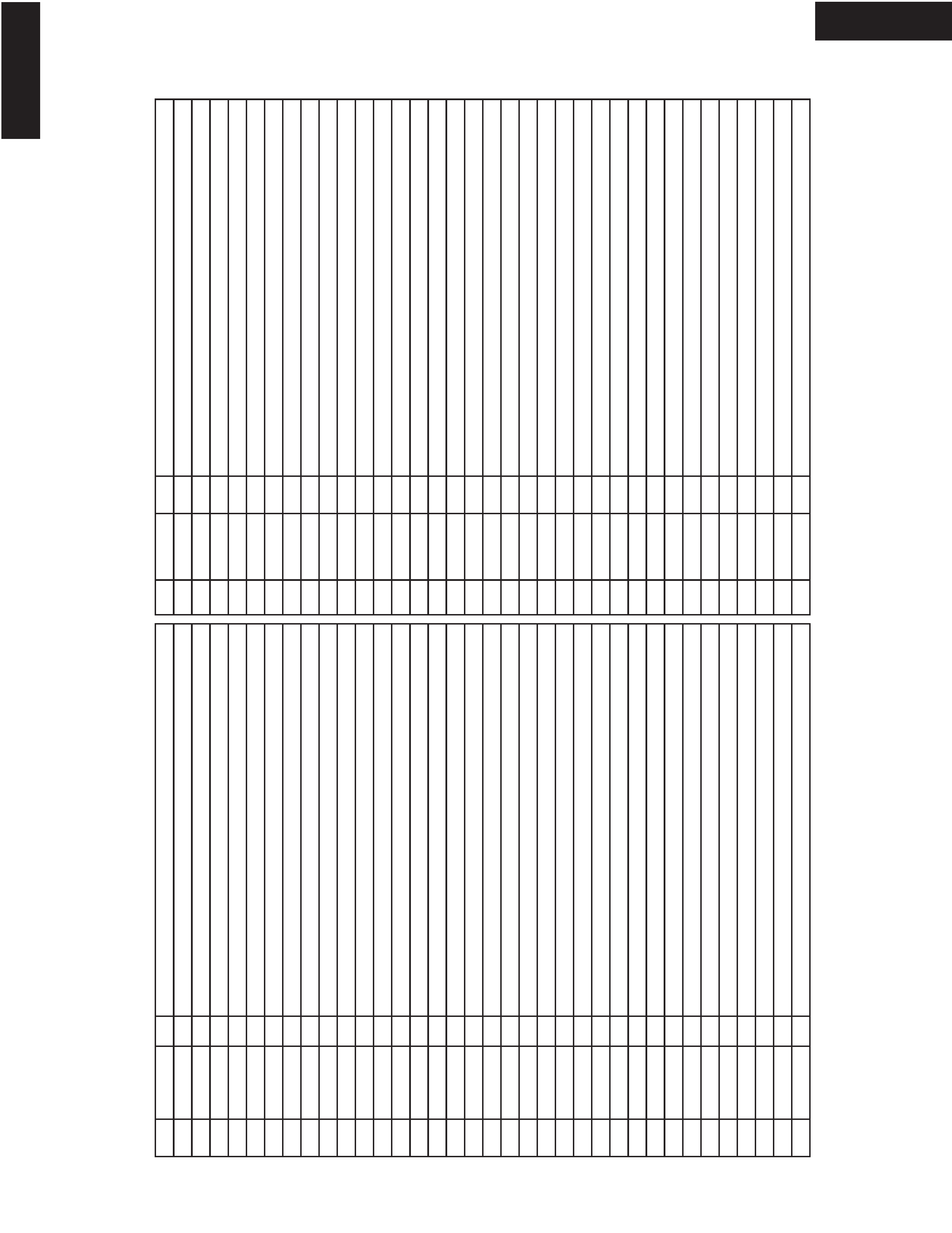
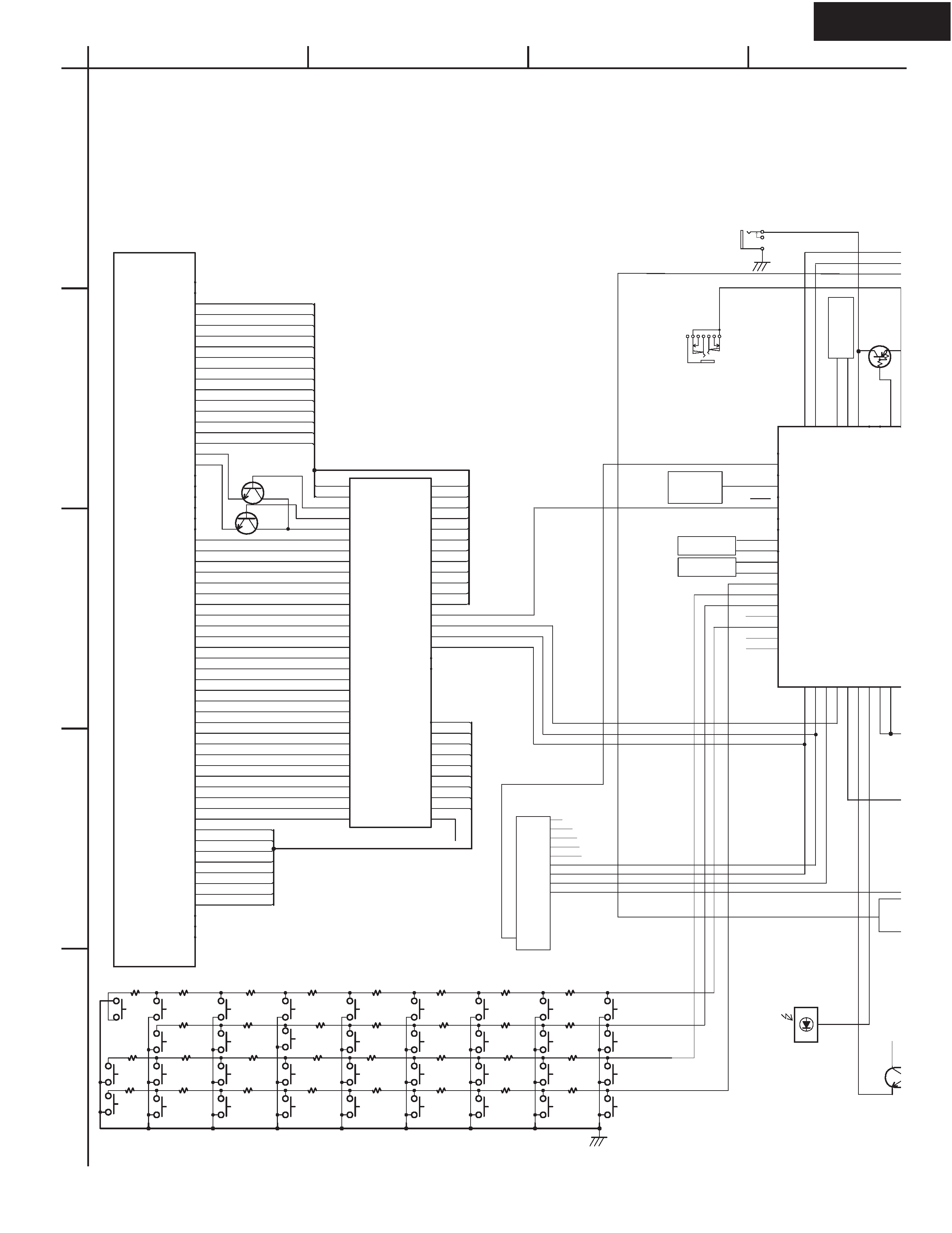
SUB MICROPROCESSOR-TERMINAL DESCRIPTION
DTC-9.4
DTC-9.4
MAIN MICROPROCESSOR-TERMINAL DESCRIPTION
DTC-9.4
No.
Function
I/O
Description
1 DSPDA
O
Serial data output pin to transfer the data to DSP, DIR, Net-tune DAC and Second PLL ICs.
2 DSPCL
O
Serial clock output pin to transfer the data to DSP, DIR and Net-tune DAC ICs.
3 TNCL
CLK Serial clock output pin for the tone control ICs.
4 Z2LMUT
O
Muting control signal output pin for line of zone 2 channel.
5 HPMUT
O
Muting control signal output pin for headphone.
6 Z2MUT
O
Muting control signal output pin for zone 2 channel when the power source is turned on.
7 AMUT
O
Muting control signal output pin of analog section.
8 VSS
External data bus width select pin.
9 VSS
Processor mode select pin
10 ~PRTCTTHM
I
Detection input pin for thermal protector. Not used.
11 SEC1H
O
Primary voltage select pin for main amplifier. Not used.
12 ~RESET
System reset input pin
13 XOUT
System clock output pin. Connect 16MHz ceramic resonator between #13 and #15.
14 VSS
Ground pin.
15 XIN
System clock input pin. Connect 16MHz ceramic resonator between #13 and #15.
16 VCC
Power supply pin. Apply 5V.
17
I
Not used.
18 PRTCTV
I
Detection input pin for protection circuit of abnormal voltage and current.
19 RDSCL
I
Serial clock input pin of RDS demodulator.
20 ~POFF
I
Power failure detection input pin.
21 ~RDSID
I
Identification input pin of RDS demodulator.
22 RDSDA
I
Serial data input pin to transfer RDS demodulator.
23 ~XPOR
O
Reset output pin to multi media microprocessor when power is turned on.
24 ~XDACS
O
Chip select output pin of DAC for Net tune.
25 ~XDARST
O
Reset signal output pin of DAC for Net tune.
26 ~TNCS1
O
Chip select output pin for tone control IC of front channel.
27 NPOWER
O
Power supply control output pin of audio circuit.
28 TNDA
O
Serial data output pin to tone control IC.
29 IICSCL
O
Serial clock output pin to Y/C, Component separation IC.
30 IICSDA
O
Serial data output pin to Y/C, Component separation IC.
31 ~XPOWER
O
Power supply control output pin. Not used.
32 ~SUBRESET
O
Reset signal output pin for sub microprocessor.
33 ~SUBPOFF
O
Power off output pin to sub microprocessor
34 ~SUBREQ
I
Transfer request signal input pin for sub microprocessor.
35 MAINSO
O
Serial data output pin to transfer data between main and sub microprocessor.
36 MAINSI
I
Serial data input pin to transfer data between main and sub microprocessor.
37 MAINSCK
O
Serial clock output pin to transfer data between main and sub microprocessor.
38 ~MAINREQ
O
Request signal output pin to transfer data between main and sub microprocessor.
39
O
Not used.
40 (2ndBTACT)
O
Not used.
41
I
Mode setting pin to write the program on flash microprocessor.
42 ~DIRCS
O
Chip select output pin to DIR(AK4114) IC.
43 ~DIRRST
O
Reset output pin to DIR IC.
44 DFS
O
DFS output pin of DAC and CODEC ICs.
45 ~DAPD
P50
O
Power down output pin of DAC.
46
I
Write mode setting pin of flash microprocessor.
47 K
I
Lock input pin of second PLL IC.
48 2NDPLLCL
O
Clock output pin to second PLL IC.
49 2NDPLLCS
O
Chip select output pin of second PLL IC.
50 EX
O
Input select output pin of net tune.
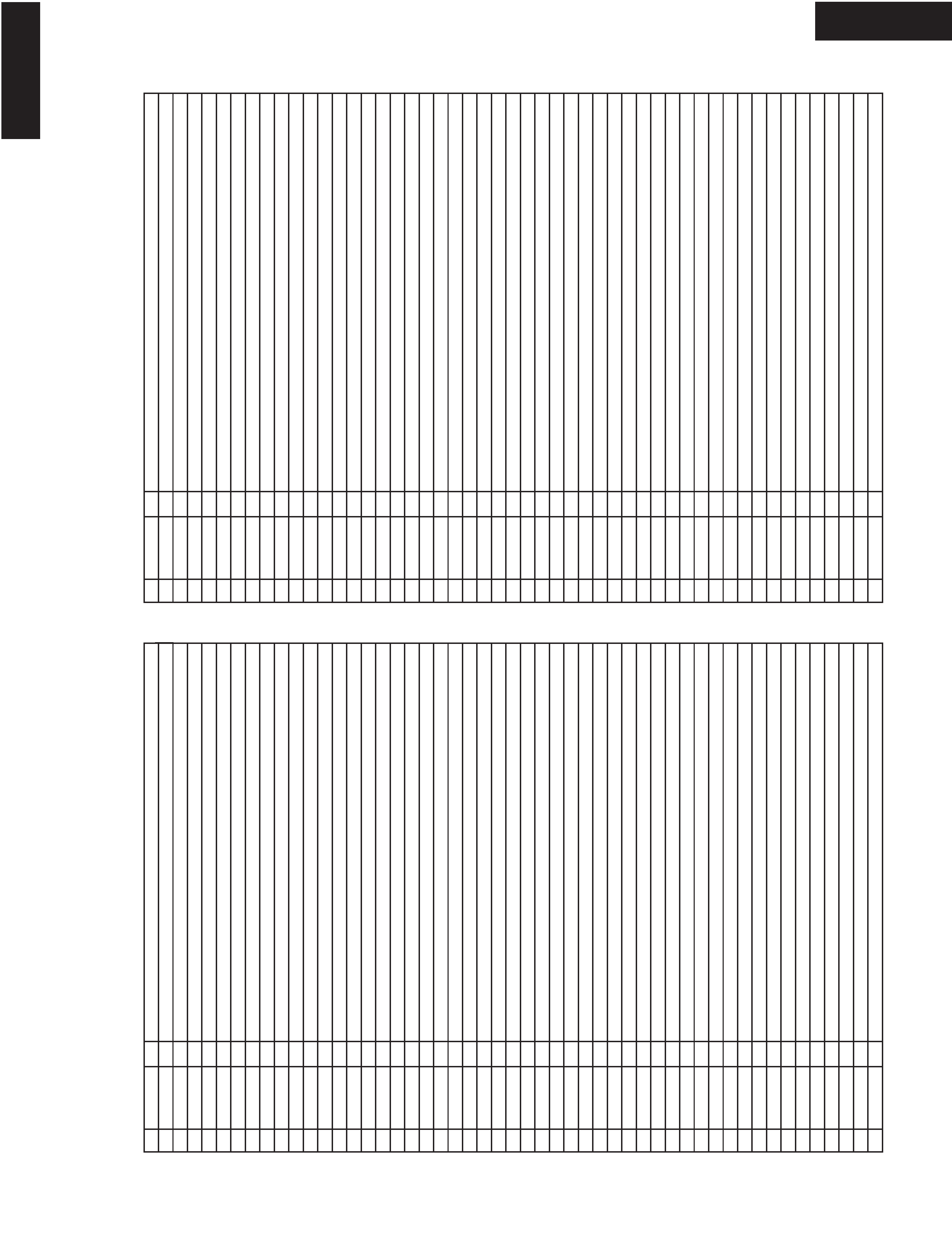
No.
Function
I/O
Description
51 ~CODECPD
O
Power down output pin of CODEC IC.
52 UPSMPL
O
Clock select output pin for up-sampling.
53 ~DSP1RST
O
Reset output pin of first DSP IC.
54 DSP1PM
O
PLL initializing output pin of first DSP IC.
55 DSP1GP8
O
PCM or Non PCM information output pin of first DSP IC.
56 DSP1BST
O
Host I/F bootstrap output pin of first DSP IC.
57 ~DSP1HCS
O
Host I/F chip select output pin of first DSP IC.
58 ~DSP2RST
O
Second DSP reset output pin.
59 DSP2BST
O
Host I/F bootstrap output pin of second DSP IC.
60 ~DSP2HCS
O
Host I/F chip select output pin of second DSP IC.
61 (2ndBOOT)
O
"L" fixed output pin.
62 VCC
Power supply pin. Apply +5V.
63 (2ndPAGESEL O
"H" fixed output pin.
64 VSS
Power supply pin. Ground
65 (HPAGE)
O
"L" fixed output pin.
66 DTCDACCL
O
Clock output pin for DAC of DTC.D
67 DTCDACCS
O
Chip select output pin for DAC of DTC.D
68 DTCDACDA
O
data output pin for DAC of DTC.D
69 (2ndGP10)
O
"L" fixed output pin.
70 ~DSP2HACN
I
Host I/F acknowledgement input pin of second DSP.2
71 ~DSP1HACN
I
Host I/F acknowledgement input pin of first DSP.1.
72 DSP2HDOUT
I
Host I/F serial data output pin to second DSP IC.
73 DIRINT1
I
INT 1 input pin of DIR IC.
74 DIRINT0
I
INT 0 input pin of DIR IC.
75 ~TNCS2
O
Chip select output pin to tone control IC.
76 VPOWER
O
Power supply relay control output pin of video circuit.
77 12VTRGB
O
12V trigger output pin B.
78 12VTRGA
O
12V trigger output pin A.
79 12VTRGZ
O
12V trigger output pin ZONE 2.
80 SPRLZ2
O
Speaker relay control output pin for Zone 2.
81 SPRLF
O
Speaker relay control output pin for all channels.
82 APOWER
O
Power supply relay control output pin of audio circuit.
83 PLLCE
O
Chip enable output pin to PLL IC.
84 TUMUT
O
Muting control output pin for tuner section.
85 ~SD
I
Detection input pin for signal strength.
86 ~STEREO
I
Detection input pin for FM stereo broadcast.
87 AFSTB
O
Strobe signal output pin of analog function switch ICs.
88 AFDA
O
Serial data output pin for function switch ICs.
89 AFCL
O
Serial clock output pin for function switch ICs.
90 VPCL
O
Serial clock output pin for electric volume and PLL ICs.
91 VPDA
O
Serial data output pin for electric volume and PLL ICs.
92 VLSTB
O
Strobe output pin of electrical volume.
93 CDT0
I
Serial data input pin for DSP and DIR ICs.
94 DSP1GP9
I
Permission information input pin to read bit stream information of first DSP.
95 DSP1GP10
I
INTREQ input pin of first DSP IC.
96 VSS
Ground pin for A/D converter.
97 VOLH
I
Input pin to measure the output voltage of main amplifier.
98 VREF
Reference voltage input pin for A/D converter.
99 VCC
Power supply pin for A/D converter.
100 DSP1HDOUT
I
Serial data output pin of host I/F of first DSP.
P57
P55
DTC-9.4
A
1
2
3
4
5
BCD
SUB MICROPROCESSOR-CONNECTION DIAGRAM
S7559
DISPLAY
S7579
ENTER
S7551
TAPE
S7573
DIMMER
S7545
VIDEO 1
S7554
CD
S7564
ZONE 2
S7572
DSP >
S7544
DVD
S7553
PHONO
S7563
REC
S7576
MENU
S7547
VIDEO 3
S7556
EXIT
S7566
STEREO
S7571
DSP <
S7543
AUDIO SEL
S7552
TUNER
S7562
Z2 LEVL>
S7577
TUNING
DOWN
S7548
VIDEO 4
S7557
PRESET >
S7567
SURROUND
S7574
FM MODE
S7541
STANDBY
/ON
S7542
PURE AUDIO
S7561
Z2 LEVL<
S7578
TUNING UP
S7549
VIDEO 5
S7558
PRESET <
S7568
THX
S7575
MEMORY
S7546
VIDEO 2
S7555
NET
S7565
OFF
K0
K1
K2
K3
12
11
10
9
8
7
6
5
4
3
2
1
18
17
15
16
31
30
29
28
27
26
25
24
23
19
32
22
21
20
14
13
Q7503
F2
F2
NP
NP
NC
P35
P34
P33
P32
P31
P30
P29
P28
P27
P26
P25
P24
P23
P22
P21
P20
P19
P18
P17
P16
P15
P14
P13
P12
P11
P10
P9
P8
P7
P6
P5
P4
P3
P2
P1
NC
NC
NC
NC
NC
NC
16G
15G
14G
13G
12G
11G
10G
9G
8G
7G
6G
5G
4G
3G
2G
1G
NP
NP
F1
F1
Q7501
HNA-16MMT
1
2
3
4
5
6
7
8
9
10
11
12
13
14
15
16
17
18
19
20
21
22
23
24
25
26
27
28
29
30
31
32
33
34
35
36
37
38
39
40
41
42
43
44
45
46
47
48
49
50
51
52
53
54
55
56
57
58
59
60
61
62
63
64
65
66
Q7502
M66005FP
64
63
62
61
59
58
57
56
55
54
53
52
51
50
49
48
47
46
45
44
43
42
41
40
39
38
37
36
35
34
33
60
P27
P26
P25
P24
P23
P22
P21
P20
P19
P18
P17
P16
P15
P14
P13
P12
P11
P10
P9
P8
P7
P6
P5
P4
P3
P2
P1
16G
15G
14G
13G
-VP
P28
P29
P30
P31
P32
P33
P34
P35
1G
2G
3G
4G
5G
6G
7G
8G
9G
10G
11G
12G
FLOSDDA
FLOSDCL
FLCS1
FLRES
P7481
PHONES
Q7202
BUFFER
1
2
3
4
5
6
78
79
7
80
99
96
8
9
88
87
86
85
84
83
82
81
97
95
94
93
92
91
90
89
77
76
75
74
73
72
71
10
100
98
BYTE
CNVSS
MAININ
FLOSDDA
FLOSDCL
OSDCS
FLCS1
REMIN
VDDA
DIMPWM
HPDET
MAINREQ
SUBPOFF
RI
OPTO4
NETTUNE
AVCC
AVSS
VREF
SYNC
ISS
FLRES
K3
K2
K1
K0
12V,DIM
TUNER
OSDDATA
SW4
SW3
SW2
SW1
RST
OSDSCK
OSDCS
VSYNCOUT
XTALOUT2
XTALIN2
HSYNCOUT
XTALOUT1
XTALIN1
Vss
Q2001
LC74761M
1
2
3
4
5
6
7
8
9
10
11
12
13
14
15
U7201
REMOTE SENSOR
Q
P
+B
Q2
VID
SW
INITIALIZING
29
SYNCDET
Y SIGNAL
DETECTOR
CIRCUIT
INITIALIZING
INITIALIZING
SYSOUT
P36
Q7504
P204
RI
VIDEO
ZONE2